Article

A Learning-Based Framework for Circuit Path Level NBTI Degradation Prediction

National ASIC System Engineering Research Center, School of Electronic Science and Engineering, Southeast University, Nanjing 210000, China
*
Author to whom correspondence should be addressed.
Electronics 2020, 9(11), 1976; https://doi.org/10.3390/electronics9111976
Submission received: 17 October 2020 / Revised: 5 November 2020 / Accepted: 16 November 2020 / Published: 22 November 2020
(This article belongs to the Section Circuit and Signal Processing)

Abstract

:
Negative bias temperature instability (NBTI) has become one of the major causes for temporal reliability degradation of nanoscale circuits. Due to its complex dependence on operating conditions, it is a tremendous challenge to the existing timing analysis flow. In order to get the accurate aged delay of the circuit, previous research mainly focused on the gate level or lower. This paper proposes a low-runtime and high-accuracy machining learning framework on the circuit path level firstly, which can be formulated as a multi-input–multioutput problem and solved using a linear regression model. A large number of worst-case path candidates from ISCAS’85, ISCAS’89, and ITC’99 benchmarks were used for training and inference in the experiment. The results show that our proposed approach achieves significant runtime speed-up with minimal loss of accuracy.

1. Introduction

Invasive uninterrupted scaling of CMOS and fin field-effect transistor (FinFET) technologies to nanoscale level leads to various fallouts such as variability of process parameters and aging [1]. Fabrication-induced geometric and electrical parameter variations, e.g., changes in device effective channel length and threshold voltage, have introduced large-scale variability of circuit performance. Meanwhile, runtime aging effects, such as electromigration, thermal cycling, and negative bias temperature instability (NBTI), have become another serious concern in nanoscale integrated circuit design [2].
NBTI is known to be the most critical reliability issue that can affect circuit lifetime [3,4]. NBTI occurs when a pMOS device is under negative bias conditions (Vgs = −Vdd), especially at high temperatures. Due to NBTI, the threshold voltage (|Vth|) of the transistor increases with time, resulting in a reduction in drive current. The reduction in drive current in turn results in temporal degradation in the performance of a circuit, causing reliability degradation over time, and may eventually cause the circuit to fail. On the contrary, when the pMOS is off (Vgs = 0), |Vth| will decrease gradually before stress injection, and pMOS degradation is relaxed. This condition is defined as the recovery phase of NBTI. Degradation caused by NBTI increases gradually repeating stress and recovery cycles [5].
Obviously, an early estimation of reliability is necessary in the design phase and should be considered as one of the design parameters to ensure the reliable operation of circuits for a desired period of time. To facilitate the reliability analysis process, considerable efforts have been put into estimating the circuit performance degradation. As a result, many researchers have begun analyzing these effects at the transistor and gate level in order to enable the evaluation of larger circuit. Nevertheless, an approach which can analyze the temporal degradation using a low-runtime and high-accuracy method at the circuit level directly has yet to evolve. The central objective of this paper is to propose a regression-based machine learning algorithm in high level due to NBTI effects, which is the first such paper in the literature to the best of the authors’ knowledge.
The rest of the article is organized as follows: Section 2 introduces the related research on NBTI degradation comprehensively from physical to circuit level. Section 3 introduces the general idea of the work. Section 4 describes in detail the proposed framework. Section 5 reports the experimental results. The paper is concluded in Section 6.

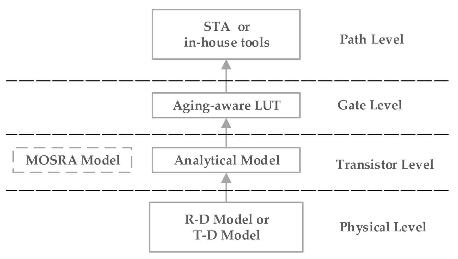
2. Literature Review on NBTI Degradation Research

The growing concern of device failure due to NBTI has prompted a significant effort on the part of the research community, including but not limited to the content shown in Figure 1. For example, the aging measurement method [6,7,8,9] does not appear in Figure 1, which also belongs to the aging domain.

2.1. Physical Level

Two prevalent physical mechanisms, reaction–diffusion (R–D) [10,11] and trapping–detrapping (T–D) [12], have been proposed in the literature to explain NBTI. Because T–D has not been fully proven, the R–D model is widely used to interpret the NBTI mechanisms [13]. According to the R–D model, in conventional pMOS, due to crystal mismatch at the Si–SiO2 interface, traps are present in the form of Si dangling bonds after the growth of gate oxide. Positive interface traps are generated due to disintegration of silicon–hydrogen (Si–H) bonds and one H atom that can diffuse away from the interface under negative bias conditions, as shown in Figure 2a. As a result, the threshold voltage increases and the pMOS transistor becomes slower and fails to meet timing constraints. Once the stress is removed, the H near the Si/SiO2 interface will anneal the broken Si-bonds, as shown in Figure 2b, where two interface traps disappear, leading to a partial recovery of the degradation. The amount of recovery is highly related to the frequency, duty cycle, the magnitude of bias change, etc.

2.2. Transistor Level

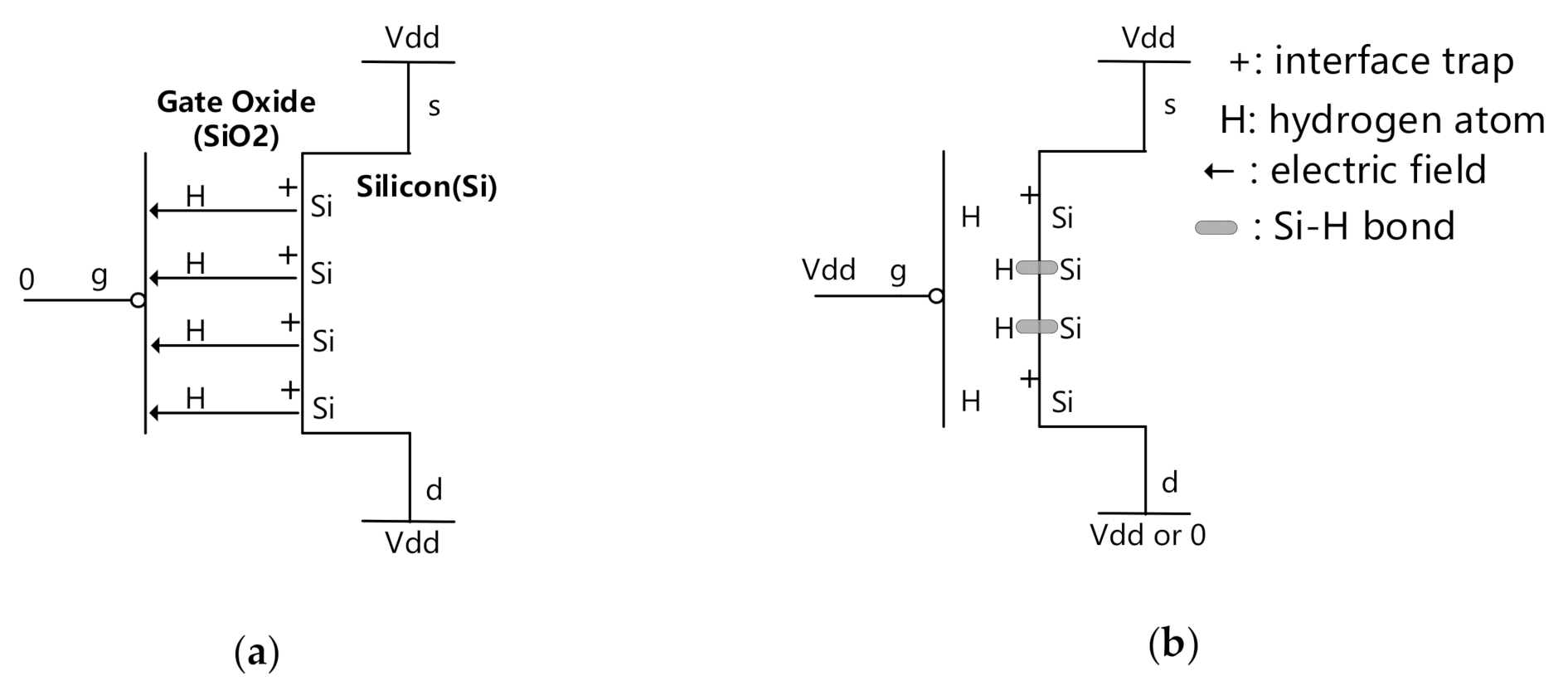
2.2.1. NBTI Analytical Model

From the numerical solution of the standard reaction diffusion (R–D) model, the NBTI degradation models were developed, which formed the basis for higher-level research.
In [14], the NBTI-related increase in the threshold voltage of a pMOS transistor in the continuous stress phase from t 0 to t , i.e., static NBTI, was evaluated using Equation (1).
Δ V t h = K v 2 . t t o 1 / 2 + Δ V t h 1 2 + δ v ,
where
K v = A N B T I × t o x × C o x V d d V t h × e ( V d d V t h t o x × E 0 E a k × T ) ,
where Δ V t h 1 is the change in threshold voltage that pMOS already exhibits at time t 0 ,   t o x is the oxide thickness, and C o x is the gate capacitance per unit area. E 0 and E a are device-dependent parameters and constant. A N B T I is a technology-dependent constant, and k is the Boltzmann constant. T is the temperature in K . δ v is a constant added to include the impact of oxide traps and other charge residues.
In a realistic working circuit, the gate voltage of pMOS will periodically change. When Vgs = 0, the pMOS transistor is placed in the recovery phase, and the threshold-voltage drift is partially recovered. Equation (3) shows the final change in the threshold voltage of a pMOS transistor [14] assuming the recovery happens at t 0 , i.e., dynamic NBTI.
Δ V t h = Δ V t h 1 δ v 1 η t t 0 / t ,
where η is a constant 0.35.
In order to predict a long-term dynamic NBTI effect, an updated model was proposed [15], which includes the recovery effect and is useful for the estimation of degradation by years. In this model, the V t h   degradation after time t has passed ( Δ V t h , t ) is expressed as Equation (4).
Δ V t h , t = K v 2 . T c l k . α 1 β t 1 / 2 n 2 n ,
where T c l k is the clock period, and α is the stress probability of pMOS. Here, stress probability is defined as time ratio of stress phase in one clock period, i.e., (time of stress)/(time of stress + time of recovery). Stress probability is sometimes also named duty cycle. β t is a parameter that has a dependence on temperature, T c l k , α , and t . The specific formula of β t   is detailed in the literature [15]. n is equal to 0.25. When the operating frequency is higher than 10 kHz, there is little relation between Δ V t h , t and T c l k [15]. In this case, the relationship between Δ V t h , t   and α can be formulated as Equation (5).
Δ V t h , t 0.001 n 2 K v 2 α C t 0.81 t o x 2 1 α n ,
where parameter C is dependent on temperature. The specific formula of C is detailed in the literature [15].

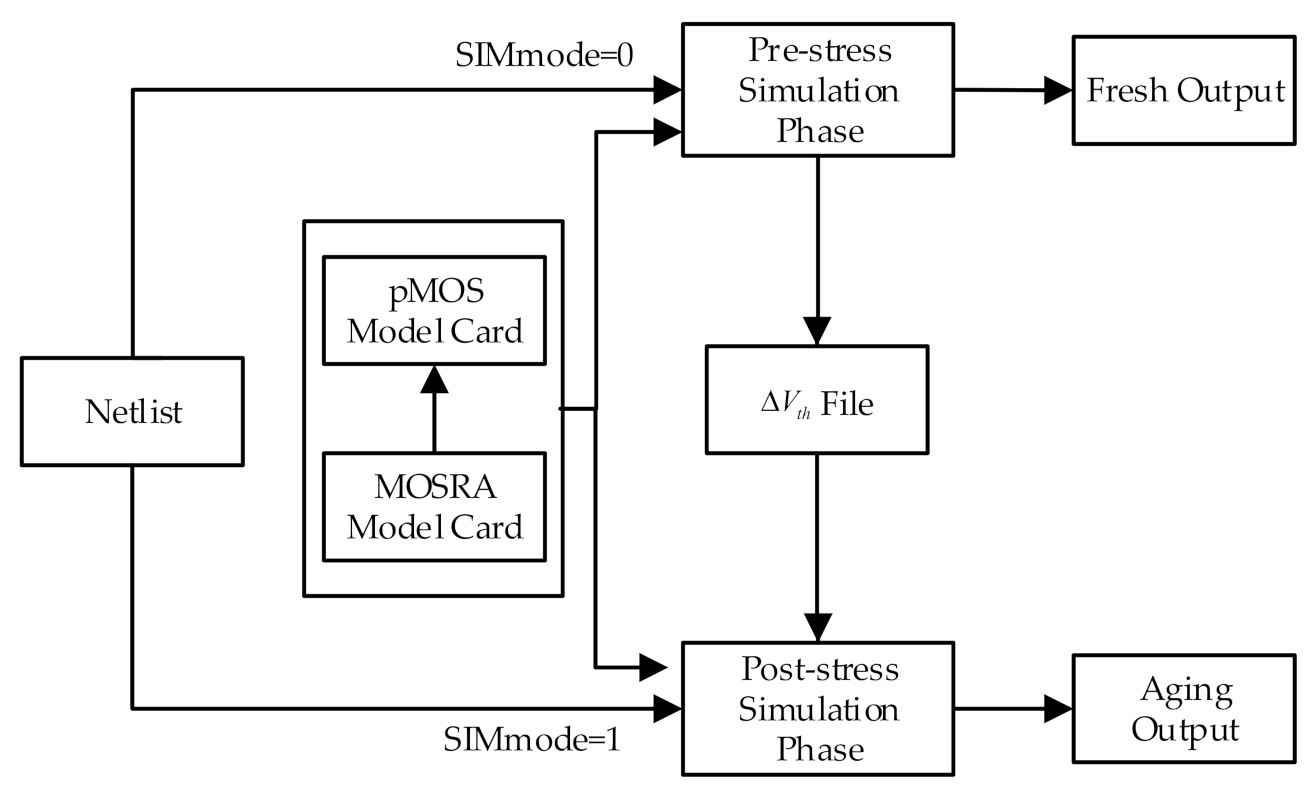
2.2.2. MOSFET Model Reliability Analysis (MOSRA) Aging Model

To simulate the effect of NBTI, an efficient simulation analysis and an accurate aging model are required to translate the amount of electrical stress into device parameter degradation. There are three major industry-standard aging simulators, namely, Hewlett simulation program with integrated circuit emphasis (HSPICE) MOSRA from Synopsys, RelXpert from Cadence, and Eldo from Mentor Graphics [16]. In this work, we used MOSRA to model the circuit degradation behavior in the experiment.
MOSRA is the built-in aging model integrated into Synopsys HSPICE, which can be used to predict the long-term reliability and performance of the circuit. Recently, MOSRA was deployed in many studies for reliability simulation and circuit design using the Synopsis HSPICE platform [17,18,19]. It should be noted that the MOSRA model itself is also constructed on the basis of a specific NBTI analytic model.
Here, it is useful to briefly review how degradation is calculated by the MOSRA model. The working of MOSRA takes place in two phases, i.e., the pre- and post-stress simulation phases [20,21]. The pre-stress simulation phase is also known as the fresh simulation phase, where the electrical stress of every user-selected metal oxide semiconductor field effect transistor (MOSFET) is computed by HSPICE on the basis of the circuit behavior and the built-in MOSRA models. Then, the post-stress simulation phase is executed. The post-stress simulation simulates the degradation effect on the circuit performance on the basis of the result attained from the pre-stress simulation. After that, the result of the circuit performance is obtained, such as the circuit delay.
A simplified procedure for HSPICE MOSRA is shown in Figure 3. When SIMmode = 0, only the pre-stress simulation is selected. In addition to outputting some fresh results, a Δ V t h file with the suffix radeg0 is also included. When SIMmode = 1, only the post-stress simulation is selected. In this phase, HSPICE uses the Δ V t h   information in the radeg0 file and updates the pMOS device model for reliability analysis. It should be noted that SIMmode is 2 by default, where pre- and post-stress simulations are executed sequentially. It is reasonable that, even though HSPICE can automate the analysis process and is usually regarded as a gold standard for reliability analysis, the simulations are extremely time-consuming if applied to circuits of a certain scale. As for the MOSRA model, the intrinsic regressive calculation process is conducted when an aging analysis is performed to achieve high accuracy.

2.3. Gate Level

NBTI aging destroys the traditional two-dimensional assumption in modern-day static timing analysis (STA), introducing the high-dimensional correlation problem. For accurate STA for NBTI, one common method involves adding extra dimensions to the traditional two-dimensional (2D) look up table (LUT ). For example, in [22], the extracted delay information, such as gate delay and output transition time, was stored in n + 4-dimensional LUTs. The n + 4-dimension is defined as (1) V t h shifts of different transistors (n transistors corresponding to n dimensions in the LUT) inside the cell, (2) input slope, (3) output load, (4) temperature, and (5) voltage. For dimensionality reduction, [23] proposed three-dimensional (3D) LUTs, including three input variables: input slew, capacitive load, and NBTI stress probability.
As discussed above, aging adds new challenges to the existing timing analysis flow, as it complicates the simple variation model assumed by the modern timing libraries. As a possible solution, learning-based timing characterization is under active research. The authors of [24] proposed a learning-based method for predicting the NBTI-induced delay degradation in large designs like processors. The training design contains tens of thousands of training samples, and the sample is a gate delay associated with a particular set of predictor parameters. Although the work in [24] used a machine learning method, it essentially constructed an aging-aware 3D LUT for each cell as proposed in [23]; thus, the author also classified it as an aging-aware LUT.
In general, each cell in the technology library file is characterized using accurate HSPICE simulations when the threshold-voltage drift of a pMOS transistor is calculated by the NBTI analytical model, which also applies to the literature [24], because each training sample also needs HSPICE simulations to obtain the gate delay. Hence, these methods have a high library characterization overhead. In addition, the traditional two-dimensional LUT has inherently inaccurate estimations caused by the interpolation and extrapolation methods. This problem becomes more serious with higher dimensionality.

2.4. Path Level

The performance degradation result of the circuit can be obtained through integrated software, such as STA tools and in-house tools, which essentially encapsulate the lower level technology as discussed above. Once the netlist of the circuit is entered, an increase in path delay can be obtained. The specific implementation process is not described in detail here.
The above approaches and tools are either inaccurate or extremely time-consuming for long-range aging simulations. In searching for a low-runtime and high-accuracy solution for aging-aware circuit path delay estimation, we utilized regression-based machine learning algorithms in path level firstly. Compared with the traditional method, the solution proposed in this paper is directly oriented toward the circuit path, which does not need to consider the implementation details of the gate level and below.

3. Main Idea

In order to study the aging characteristics of the circuit and find the hidden rules, sufficient experiments were implemented on the basis of ISCAS’85, ISCAS’89, and ITC’99 benchmark circuits. The MOSRA model was applied to a certain number of worst-case path candidates from c7552 within ISCAS’85 for aging-aware delay degradation over 10 years in time steps of 1 year at a temperature of 400 K. The HSPICE simulation results are shown in Figure 4. For each curve, 11 time points, including the fresh time at time = 0, are marked on the horizontal axis. The vertical axis represents the aged delay corresponding to each time point. The detailed experimental process can be found in Section 4.
It can be observed that the path delay changes in the first year were relatively large, while the degradation speed in the subsequent years slowed down. In addition, there were high similarities in the changing trends among different benchmark circuit paths, which could be well utilized by machine learning. The characterized path delay, collected from HSPICE simulations or real chip measurements, could be trained as the sampling set. For a new path, inference could be made on the basis of a small amount of known data, thereby reducing the cost of the entire path characterization.

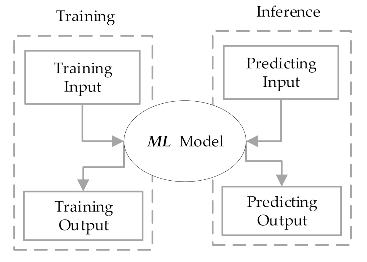
4. Proposed Learning-Based Framework

An overview of the proposed framework is shown in Figure 5, where ML is the abbreviation of machine learning. Similar to the traditional machine learning architecture, the framework mainly consisted of two stages: training and inference. The training sample set contained two parts: input and output. Each training input corresponded to a training output. The available machine learning model could be obtained by training; then, the inference process could predict the unknown result.
Taking Figure 4 as an example, we first divided the curves into two categories: TR = {tri, 1 ≤ io} for training, i.e., where the delay of all the time points on the curve was already known, and PR = {prj, 1 ≤ jp}, i.e., where the aged delay corresponding to only a few time points on the curve was already known, but most other time points needed to be predicted. Therefore, we needed to distinguish the time points on the horizontal axis.
Suppose there are n time points on the horizontal axis; then, the set is denoted as X, which is divided into two categories: XI = {xix, 1 ≤ xm}, XO = {xoy, 1 ≤ yn-m}. The difference between xix and xoy is that, for any curve prj, the aged delay corresponding to xix, denoted as d x i x p r j , is known, while the aged delay corresponding to xoy, denoted as   d x o y p r j , is to be predicted. As for the curve tri, the aged delays of xix and xoy, denoted as d x i x t r i ,   d x o y t r i respectively, are all known. It should be noted that xix and xoy can be sorted crosswise on the horizontal axis.
Now, the problem we want to solve is that, given a curve prj to be predicted, the d x i x p r j value of any time point xixXI is known, and we need to predict the   d x o y p r j corresponding to all other time points xoyXO. The corresponding machine learning model form is
d ^ x o 1 p r j , d ^ x o 2 p r j , ,   d ^ x o n m p r j = ML ( d x i 1 p r j , d x i 2 p r j , , d x i m p r j ) ,
where d ^ x o y p r j is the predicted output corresponding to xoy on the curve prj, and ML represents a machine learning model.
For utilizing the similarity between curve tri and prj, and reducing the training set space, this article drew on research results from the literature [25]. To build this model, from the point of view of machine learning, the training sample sets were constructed as shown in Equation (7), where TRin and TRout are the training input and training output blocks in Figure 5.
T R i n = d x i 1 t r 1   d x i 2 t r 1     d x i m t r 1 d x i 1 t r 2   d x i 2 t r 2     d x i m t r 2 .           .           .         . .           .           .         . .           .           .         . d x i 1 t r o   d x i 2 t r o     d x i m t r o ,
T R o u t = d x o 1 t r 1   d x o 2 t r 1     d x o n m t r 1 d x o 1 t r 2   d x o 2 t r 2     d x o n m t r 2 .   .   .   . .   .   .   . .   .   .   . d x o 1 t r o   d x o 2 t r o     d x o n m t r o .
Unlike the traditional regression model, this is a multi-input–multioutput regression model, which was developed using Python and scikit-learn libraries, such as linear regression, k-nearest neighbor regression, and random forest regression. After this model was trained, we could perform inference. The predicting sets were constructed as shown in Equation (8), where INFin and INFout are the predicted input and predicted output blocks in Figure 5. During the inference process, INFin only represented one row or several rows of data at the same time.
I N F i n = d x i 1 p r 1   d x i 2 p r 1     d x i m p r 1 d x i 1 p r 2   d x i 2 p r 2     d x i m p r 2 .           .           .         . .           .           .         . .           .           .         . d x i 1 p r p   d x i 2 p r p     d x i m p r p ,
I N F o u t = d ^ x o 1 p r 1   d ^ x o 2 p r 1     d ^ x o n m p r 1 d ^ x o 1 p r 2   d ^ x o 2 p r 2     d ^ x o n m p r 2 .   .   .   . .   .   .   . .   .   .   . d ^ x o 1 p r p   d ^ x o 2 p r p     d ^ x o n m p r p .
Taking Table 1 as an example, it can be seen that there were four training samples from TR = {tri, 1 ≤ i ≤ 4} and one predicting curve, while there were eight time points on each curve, where XI = {xix, 1 ≤ x ≤ 3}, XO = {xoy, 1 ≤ y ≤ 5}. The data in the grid represent the delay of each circuit path corresponding to time points xi1–xi3 and xo1–xo5. According to the previous description, TRin, TRout, and INFin were defined as shown in Equations (9) and (10), while INFout was composed of five predicting dates, represented as “^” in Table 1.
T R i n = 9.077   9.102   9.111 8.850   8.875   8.884 8.831   8.855   8.863 8.825   8.848   8.857 ,
T R o u t = 9.105   9.108   9.110   9.113   9.114 8.879   8.881   8.882   8.885   8.886 8.858   8.860   8.862   8.865   8.866 8.852   8.854   8.856   8.858   8.859 ,
I N F i n = 8.726   8.749   8.757 .

5. Numerical Experiment

5.1. Circuit Level Experiment Setup

We evaluated the learning-based chip age prediction model on a subset of benchmark circuits. The circuits were synthesized using a Synopsys Design Compiler with Nangate 45 nm Open Cell Library. We selected 30 worst-case path candidates from c499, c6288, and c7552 within the ISCAS’85 benchmark, s13207, s15850, and s38584 within the ISCAS’89 benchmark, and b04, b08, and b14 within the ITC’99 benchmark using PrimeTime tool. These candidates constituted training sample sets and predicting sets. Other parameters were as follows: TR = {tri, 1 ≤ i ≤ 10}, PR = {prj, 1 ≤ j ≤ 20}, XI = {xix, 1 ≤ x ≤ 3}, and XO = {xoy, 1 ≤ y ≤ 8}, where xi1, xi2, and xi3 correspond to 0 years, 1 years, and 5 years.
As discussed above, circuit aging depends on the operating conditions, such as temperature, voltage, and stress probability. For simplicity, we fixed the year of aging and temperature at 10 years and 400 K for NBTI during the experiment. The input signal source is described in Table 2, including the static and dynamic NBTI effects. As for the dynamic NBTI effect, different types of stress probability are listed. We then used Synopsys HSPICE to capture the aging effects of the critical path candidates.
The prediction accuracy was measured according to two types of error, the relative root-mean-square error (rRMSE) and the mean absolute error (MAE), which were calculated using the following equations:
r R M S E = 1 n m y = 1 n m ( d ^ x o y d x o y d x o y ) 2 × 100 % ,
M A E = 1 n m y = 1 n m d ^ x o y d x o y ,
where d ^ x o y   and   d x o y   are the predicted and real outputs at xoy of the curve.
In this article, it was stipulated that each predicting circuit path corresponded to a rRMSE or a MAE. A lower error denoted the better prediction and fitting performance of the learning method.

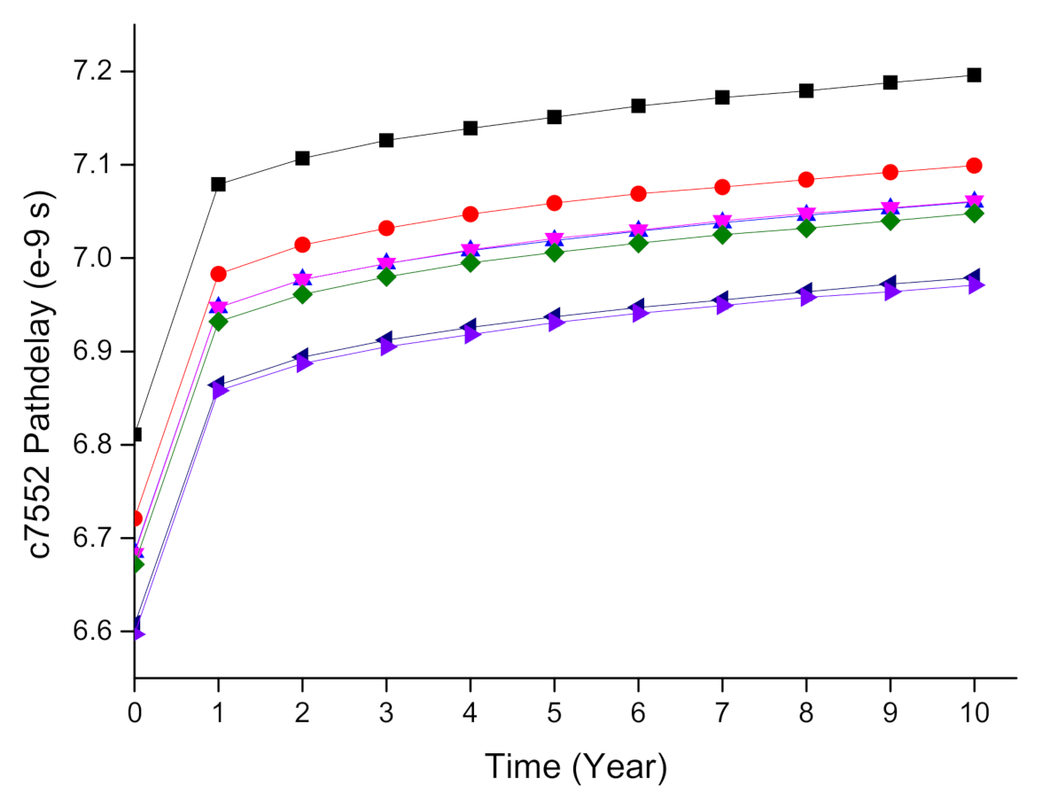
5.2. Experiment Result

5.2.1. Static NBTI Condition

We considered the static NBTI first, i.e., case 1 shown in Table 2. During the experiment, the accuracy of the machine learning prediction and the running performance were the two key evaluation points. The experimental results are listed in Table 3, Table 4 and Table 5, where rRMSE and MAE are the average values of all prj (1 ≤ j ≤ 20) using the linear, k-nearest neighbor, and random forest regression methods, while runtime is the time spent on the critical path by the three regression methods and HSPICE. Each evaluation was applied to the benchmark circuits mentioned above. Here, we list the three circuits from ISCAS’85, ISCAS’89, and ITC’99 benchmark. It should be noted that the runtime under each case fluctuated in a small range with different operations; thus, the runtime here can be regarded as an average value.
It can be seen from Table 3, Table 4 and Table 5 that the error obtained using linear regression, whether for rRMSE or MAE, was relatively concentrated, while that obtained using the other two methods was divergent. As for MAE, linear regression provided the lowest error level in each circuit case, improved by one or two orders of magnitude compared with the other two regression models. The rRMSE result showed a similar improvement.
In terms of runtime, the computation overhead could be significantly reduced by adopting any regression method. In fact, the time spent in HSPICE simulation was greatly related to the complexity of the critical path, while the time spent in regression methods remained basically unchanged. For different critical paths, the runtime ratio between HSPICE and linear regression changed significantly. A longer critical path resulted in a more obvious improvement effect of runtime caused by the regression method.
Considering the two factors of prediction accuracy and central processing unit (CPU) runtime, it can be concluded that the linear regression, achieving the highest prediction accuracy with minimal computation overhead, was more suitable for solving the problem than the k-nearest neighbor and random forest regression methods. On the other hand, it also illustrated the highest similarity among the curves.
In order to more intuitively observe the accuracy of linear regression prediction, MAE could be used. Taking the critical paths from c499, c6288, and c7552 as examples, the data obtained using the model prediction and the actual values are shown in Figure 6. Excellent predictability was observed between the predicted and the real data.

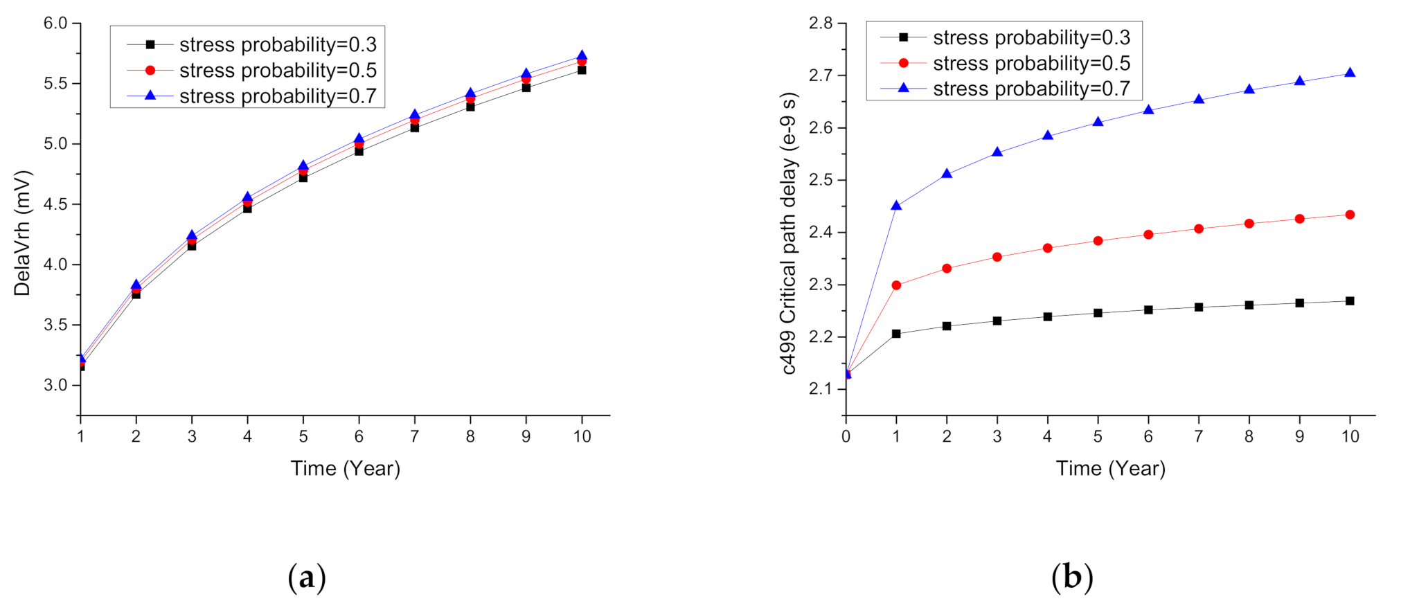
5.2.2. Dynamic NBTI Condition

Next, we focused on the linear regression and checked its performance for dynamic NBTI corresponding to case 2, case 3, and case 4, as presented in Table 2.
Taking the critical path from c499 as an example, the relationship among the Δ V t h , t of one pMOS, the path delay, and the NBTI stress probability is shown in Figure 7. It can be seen that the Δ V t h , t   and path delay increased as the stress probability increased due to the overall stress time increasing. This conclusion also applied to the critical paths from c6288 and c7552.
The prediction accuracy and runtime verification was performed using different types of NBTI stress probability, and the experimental results are shown in Table 6, Table 7 and Table 8.
It can be seen that the accuracy and runtime of linear regression showed good consistency under dynamic NBTI conditions. Compared to the static NBTI condition, rRMSE and MAE had almost the same accuracy level. However, the runtime of HSPICE was significantly longer, and the variation in linear regression was relatively small, showing that the linear regression had better speedup here.

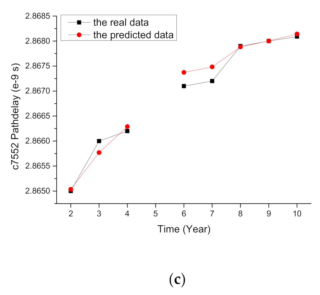
5.2.3. Comparison with Other Studies

Similarly to [23,24], our work also used the Nangate 45nm Open Cell Library, assuming 400 K and 10 years of operation during the experiment, and the simulation results of HSPICE were used to verify the accuracy and runtime performance. In [18,19], the aged delay of each circuit path in the designated 10th year was measured (corresponding to d ^ x o 8 in this paper) and then compared with the HSPICE date (corresponding to the d x o 8   ). The obvious difference is that [23,24] calculated the aged path delay using the LUT method, while our proposed method was a machining learning framework at the circuit path level.
In order to verify our proposed method, we compared our experimental results with [23] and [24], as shown in Table 9. In [23], the numerical experiments were conducted on a circuit design, while, in [24] and this paper, a set of designs was used, where we only considered the worst case.
The technique in [23] took a total of 14 s to calculate all path delays, and the average time was approximately 0.00055 s. From the experimental data, it can be judged that our proposed method had better performance in terms of prediction accuracy and runtime.

6. Conclusions

Traditional circuit aged delay is mostly based on the LUT scheme. Each cell in the library is characterized by accurate HSPICE simulations, which clearly result in high computation overhead. This paper proposed a novel learning-based aged delay prediction method at the circuit level. The experimental results showed that the framework with linear regression could greatly reduce the runtime while ensuring accuracy.
It should be noted here that the proposed method has a precondition, i.e., the input signal is very regular, whether under static or dynamic NBTI conditions. However, for some very special workloads which cannot be expressed in the manner shown in Table 2, even if the usable training sample sets are available, the application effect of the method remains to be verified.
During the experiment, we found that, when the model trained on one benchmark circuit was directly used for inference on another benchmark circuit, the prediction accuracy decreased. Furthermore, this study was not extended to experiments using real silicon. We will address these issues in future research.

Author Contributions

Conceptualization, A.B.; software, A.B.; data curation, A.B.; writing—original draft preparation, A.B.; writing—review and editing, A.B.; supervision, J.L.; project administration, J.L.; funding acquisition, J.L. All authors have read and agreed to the published version of the manuscript.

Funding

This work was supported in part by the National Key Research and Development Program of China under Grant 2019YFB2205004, the National Natural Science Foundation of China under Grant 61834002, and the Jiangsu Natural Science Foundation under Grant SBK2020022894.

Conflicts of Interest

The authors declare no conflict of interest.

References

  1. Khalid, U.; Mastrandrea, A.; Olivieri, M. Effect of NBTI aging and process variations on write failures in CMOS and FinFET flip-flops. Microelectron. Reliab. 2015, 55, 2614–2626. [Google Scholar] [CrossRef] [Green Version]
  2. Lu, Y.H.; Shang, L.; Zhou, H.; Zhu, H.L.; Yang, F.; Zeng, X. Statistical reliability analysis under process variation and aging effects. In Proceedings of the 2009 46th Design Automation Conference, San Francisco, CA, USA, 26–31 July 2009; pp. 514–519. [Google Scholar]
  3. Nur, A.Z.; Hanim, H.; Muhamad, F.Z.; Abdul, K.H. Investigation of negative bias temperature instability (NBTI) effects on standard cell library circuits performance. In Proceedings of the 2019 IEEE Regional Symposium on Micro and Nanoelectronics, Genting Highland, Pahang, Malaysia, 21–23 August 2019; pp. 30–33. [Google Scholar]
  4. Hussam, A.; Victor, M.; Jörg, H. Estimating and optimizing BTl aging effects: From physics to CAD. In Proceedings of the 2018 International Conference on Computer-Aided Design, San Diego, CA, USA, 5–8 November 2018; pp. 1–6. [Google Scholar]
  5. Hiroaki, K.; Yukio, M.; Masanori, H.; Takao, O. Comparative study on delay degrading estimation due to NBTI with circuit/instance/transistor-level stress probability consideration. In Proceedings of the 11th International Symposium on Quality Electronic Design, San Jose, CA, USA, 22–24 March 2010; pp. 646–651. [Google Scholar]
  6. Denais, M.; Parthasarathy, C.; Ribes, G.; Rey-Tauriac, Y.; Revil, N.; Bravaix, A.; Huard, V.; Perrier, F. On-the-fly characterization of NBTI in ultra-thin gate oxide PMOSFET’s. In Proceedings of the 2004 IEEE International Electron Devices Meeting, San Francisco, CA, USA, 13–15 December 2004; pp. 109–112. [Google Scholar]
  7. Chaudhary, A.; Mahapatra, S. A physical and SPICE mobility degradation analysis for NBTI. IEEE Trans. Electron Devices 2013, 60, 2096–2103. [Google Scholar] [CrossRef]
  8. Sun, H.C.; Huang, C.F.; Chen, Y.T.; Wu, T.Y.; Liu, C.W.; Hsu, Y.J.; Chen, J.S. Threshold voltage and mobility extraction of NBTI degradation of Poly-Si thin-film transistors. IEEE Trans. Electron Devices 2010, 57, 3186–3189. [Google Scholar] [CrossRef]
  9. Herfst, R.W.; Schmitz, J.; Scholten, A.J. Simultaneous extraction of threshold voltage and mobility degradation from on-the-fly NBTI measurements. In Proceedings of the 2011 International Reliability Physics Symposium, Monterey, CA, USA, 10–14 April 2011; pp. XT.6.1–XT.6.4. [Google Scholar]
  10. Krishnan, A.T.; Chancellor, C.; Chakravarthi, S.; Nicollian, P.E. Material dependence of hydrogen diffusion: Implications for NBTI degradation. In Proceedings of the 2005 IEEE International Electron Devices Meeting, Washington, DC, USA, 5 December 2005; pp. 688–691. [Google Scholar]
  11. Mahapatra, S.; Goel, N.; Desai, S.; Gupta, S.; Jose, B.; Mukhopadhyay, S.; Joshi, K.; Jain, A.; Islam, A.E.; Alam, M.A. A comparative study of different physics based NBTI models. IEEE Trans. Electron Devices 2013, 60, 901–916. [Google Scholar] [CrossRef]
  12. Tibor, G.; Wolfgang, G.; Victor, S.; Ben, K. The universality of NBTI relaxation and its implications for modeling and characterization. In Proceedings of the 45th Annual IEEE International Reliability Physics Symposium, Phoenix, AZ, USA, 15–19 April 2007; pp. 268–280. [Google Scholar]
  13. Naphade, T.; Goel, N.; Nair, P.R.; Mahapatra, S. Investigation of stochastic implementation of reaction diffusion (RD) models for NBTI related interface trap generation. In Proceedings of the 2013 IEEE International Reliability Physics Symposium, Anaheim, CA, USA, 14–18 April 2013; pp. XT.5.1–XT.5.11. [Google Scholar]
  14. Vattikonda, R.; Wang, W.; Cao, Y. Modeling and minimization of PMOS NBTI effect for robust naometer design. In Proceedings of the 2006 Design Automation Conference, San Francisco, CA, USA, 24–28 July 2006; pp. 1047–1052. [Google Scholar]
  15. Bhardwaj, S.; Wang, W.; Vattikonda, R.; Cao, Y.; Vrudhula, S. Predictive modeling of the NBTI effect for reliable design. In Proceedings of the 2006 IEEE Custom Integrated Circuits Conference, Jose, CA, USA, 10–13 September 2006; pp. 1047–1052. [Google Scholar]
  16. Chen, J.; Wang, S.; Tehranipoor, M. Critical-reliability path identification and delay analysis. ACM J. Emerg. Technol. Comput. Syst. 2014, 10, 12. [Google Scholar] [CrossRef]
  17. Mohamad Saofi, M.S.S.; Hussin, H.; Muhamad, M.; Abdul, W.Y. Investigation of the NBTI and PBTI effects on multiplexer circuit performances. In Proceedings of the 2020 IEEE International Conference on Semiconductor Electronics, Kuala Lumpur, Malaysia, 28–29 July 2020; pp. 49–52. [Google Scholar]
  18. Zainudin, M.F.; Hussin, H.; Halim, A.K.; Jamilah, K. Effects of permanent and recoverable component of NBTI mechanisms on flip flop circuits designed using planar MOSFET and FinFET. In Proceedings of the 2018 IEEE Symposium on Computer Applications & Industrial Electronics, Penang, Malaysia, 28–29 April 2018; pp. 145–149. [Google Scholar]
  19. Zainudin, M.F.; Hussin, H.; Halim, A.K.; Karim, J. Aging analysis of high performance FinFET flip-flop under dynamic NBTI simulation configuration. In Proceedings of the 2017 International Conference on Applied Electronic and Engineering, Kuching, Sarawak, Malaysia, 7–8 August 2017; p. 012012. [Google Scholar]
  20. Tudor, B.; Wang, J.; Chen, Z.; Tan, R.; Liu, W.; Lee, F. An accurate and scalable MOSFET aging model for circuit simulation. In Proceedings of the 12th International Symposium on Quality Electronic Design, Santa Clara, CA, USA, 14–16 March 2011; pp. 1–4. [Google Scholar]
  21. Tudor, B.; Wang, J.; Sun, C.; Chen, Z.; Liao, Z.; Tan, R.; Liu, W.; Lee, F. MOSRA: An efficient and versatile MOS aging modeling and reliability analysis solution for 45 nm and below. In Proceedings of the 10th IEEE International Conference on Solid-State and Integrated Circuit Technology, Shanghai, China, 1–4 November 2010; pp. 1645–1647. [Google Scholar]
  22. Firouzi, F.; Kiamehr, S.; Tahoori, M.; Nassif, S. Incorporating the impacts of workload-dependent runtime variations into timing analysis. In Proceedings of the 2013 Design, Automation & Test in Europe Conference & Exhibition, Grenoble, France, 18–22 March 2013; pp. 1022–1025. [Google Scholar]
  23. Bian, S.; Shintani, M.; Morita, S.; Hiromoto, M.; Sato, T. Nonlinear delay-table approach for full-chip NBTI degradation prediction. In Proceedings of the 2016 17th International Symposium on Quality Electronic Design, Santa Clara, CA, USA, 15–16 March 2016; pp. 307–312. [Google Scholar]
  24. Bian, S.; Hiromoto, M.; Shintani, M.; Sato, T. LSTA: Learning-based static timing analysis for high-dimensional correlated on-chip variations. In Proceedings of the 2017 54th ACM/EDAC/IEEE Design Automation Conference, Austin, TX, USA, 18–22 June 2017; pp. 1–6. [Google Scholar]
  25. Pan, Z.; Li, M.; Yao, J.; Lu, H.; Ye, Z.; Li, Y.; Wang, Y. Low-cost high-accuracy variation characterization for nanoscale IC technologies via novel learning-based techniques. In Proceedings of the 2018 Design, Automation & Test in Europe Conference & Exhibition, Dresden, Germany, 19–23 March 2018; pp. 797–802. [Google Scholar]
Figure 1. Negative bias temperature instability (NBTI)-related research domain.
Electronics 09 01976 g001
Figure 2. The physical mechanism of NBTI effect: (a) negative bias conditions; (b) recovery phase.
Electronics 09 01976 g002
Figure 3. MOSFET model reliability analysis (MOSRA) model execution process in Hewlett simulation program with integrated circuit emphasis (HSPICE).
Electronics 09 01976 g003
Figure 4. The c7552 aging-aware path delay.
Electronics 09 01976 g004
Figure 5. The flow of the proposed framework.
Electronics 09 01976 g005
Figure 6. The real and predicted data of critical paths: (a) c499; (b) c6288; (c) c7552.
Electronics 09 01976 g006aElectronics 09 01976 g006b
Figure 7. (a) Relationship between the Δ V t h , t and NBTI stress probability; (b) relationship between path delay and NBTI stress probability.
Electronics 09 01976 g007
Table 1. Aged delay data corresponding to time points on different curves (unit: × 10−10 s).
Path0 Years
(xi1)
1 Years
(xi2)
2 Years
(xo1)
3 Years
(xo2)
4 Years
(xo3)
5 Years
(xi3)
6 Years
(xo4)
7 Years
(xo5)
tr19.0779.1029.1059.1089.1109.1119.1139.114
tr28.8508.8758.8798.8818.8828.8848.8858.886
tr38.8318.8558.8588.8608.8628.8638.8658.866
tr48.8258.8488.8528.8548.8568.8578.8588.859
pr18.7268.749^^^8.757^^
Table 2. Different types of NBTI stress probability of the input signal source.
Signal ExpressionStress ProbabilityNBTI Mode
Case 1pwl (0ns vdd 10n vdd 10.005n 0)/Static
Case 2pulse (vdd 0 10n 20n 20n 130n 500n)0.3Dynamic
Case 3pulse (vdd 0 10n 20n 20n 230n 500n)0.5Dynamic
Case 4pulse (vdd 0 10n 20n 20n 330n 500n)0.7Dynamic
Table 3. Accuracy and runtime comparison within ISCAS’85 under static NBTI conditions. rRMSE, relative root-mean-square error; MAE, mean absolute error.
c499c6288c7552
rRMSE (%)Linear0.043550.066470.09132
k-nearest neighbor0.06770.08062.5468
random forest0.03330.4936.15
MAE (unit: × 10−9 s)linear0.0002810.0004540.000249
k-nearest neighbor0.0058490.0067200.111890
random forest0.0028480.0304020.218054
runtime (unit: s)linear0.00150.00100.0010
k-nearest neighbor0.0450.0350.037
random forest0.300.280.29
HSPICE7.77243.0891.51
Table 4. Accuracy and runtime comparison within ISCAS’89 under static NBTI conditions.
s13207s15850s38584
rRMSE (%)Linear0.009230.008890.021880
k-nearest neighbor2.74483.75351.4827
random forest1.39061.73981.4831
MAE (unit: × 10−9 s)linear0.0002860.0003170.000449
k-nearest neighbor0.0963240.1657750.0375
random forest0.0488010.076830.0393
runtime (unit: s)linear0.0010.0010.001
k-nearest neighbor0.0320.0150.027
random forest0.100.180.11
HSPICE17.4127.78287.43
Table 5. Accuracy and runtime comparison within ITC’99 under static NBTI conditions.
b04b08b14
rRMSE (%)Linear0.0071170.0090270.008589
k-nearest neighbor1.11850.98611.5987
random forest3.81642.34120.1256
MAE (unit: × 10−9s)linear0.0004310.000540.00021
k-nearest neighbor0.0763920.033250.05170
random forest0.0260640.025790.009126
runtime (unit: s)linear0.0020.0020.002
k-nearest neighbor0.0210.0320.001
random forest0.10.160.09
HSPICE16.883.38228.91
Table 6. Comparison of linear regression within ISCAS’85 under dynamic NBTI conditions.
c499c6288c7552
rRMSE (%)Case 20.0154790.0635360.008688
Case 30.0161810.0324830.014611
Case 40.0247920.0273140.006447
MAE (unit: × 10−9 s)Case 20.00048440.00084110.0003512
Case 30.00031590.00040200.0004363
Case 40.00053950.00036560.0003260
runtime (unit: s)Case 2linear0.0010.0010.001
HSPICE28.341065.51442.02
Case 3linear0.0030.0010.002
HSPICE27.62920.70400.06
Case 4linear0.0020.0020.001
HSPICE27.59909.23385.02
Table 7. Comparison of linear regression within ISCAS’89 under dynamic NBTI conditions.
s13207s15850s38584
rRMSE (%)Case 20.037250.035470.02246
Case 30.033680.038400.04346
Case 40.002940.024410.03850
MAE (unit: × 10−9 s)Case 20.00085360.00078640.0005098
Case 30.00035250.00042110.0007097
Case 40.00037850.00061080.0007053
runtime (unit: s)Case 2linear0.0010.0010.001
HSPICE66.12102.431135.46
Case 3linear0.0010.0020.002
HSPICE65.3198.351056.31
Case 4linear0.0010.0020.001
HSPICE64.2995.771018.32
Table 8. Comparison of linear regression within ITC’99 under dynamic NBTI conditions.
b04b08b16
rRMSE (%)Case 20.007150.019380.03235
Case 30.013220.022130.01684
Case 40.021250.026530.03548
MAE (unit: × 10−9 s)Case 20.00049900.00038450.0003645
Case 30.00012450.00032140.0002923
Case 40.00030250.00016310.0000985
runtime (unit: s)Case 2linear0.0010.0010.002
HSPICE59.089.21849.93
Case 3linear0.0010.0010.001
HSPICE58.159.15816.03
Case 4linear0.0010.0010.002
HSPICE56.238.92805.77
Table 9. Comparison with [23] and [24].
Proposed Method[23][24]
absolute maximum error (%)3.45.64.06
average runtime (unit: s)0.0003750.00055/
Publisher’s Note: MDPI stays neutral with regard to jurisdictional claims in published maps and institutional affiliations.

