Article

A Power Efficient Frequency Divider With 55 GHz Self-Oscillating Frequency in SiGe BiCMOS

by
Francesco Centurelli
*,
Pietro Monsurrò
,
Giuseppe Scotti
,
Pasquale Tommasino
and
Alessandro Trifiletti
Dipartimento di Ingegneria dell’Informazione, Elettronica e Telecomunicazioni, Sapienza Università di Roma, 00184 Roma, Italy
*
Author to whom correspondence should be addressed.
Electronics 2020, 9(11), 1968; https://doi.org/10.3390/electronics9111968
Submission received: 9 October 2020 / Revised: 13 November 2020 / Accepted: 18 November 2020 / Published: 21 November 2020
(This article belongs to the Section Microelectronics)

Abstract

:
A power efficient static frequency divider in commercial 55 nm SiGe BiCMOS technology is reported. A standard Current Mode Logic (CML)-based architecture is adopted, and optimization of layout, biasing and transistor sizes allows achieving a maximum input frequency of 63 GHz and a self-oscillating frequency of 55 GHz, while consuming 23.7 mW from a 3 V supply. This results in high efficiency with respect to other static frequency dividers in BiCMOS technology presented in the literature. The divider topology does not use inductors, thus optimizing the area footprint: the divider core occupies 60 × 65 μm2 on silicon.

1. Introduction

Frequency dividers are a fundamental building block in many RF and mixed-signal high-speed systems, such as frequency synthesizers, I/Q signal generators, carrier recovery systems, SerDes systems, and time-interleaved data converters [1,2,3,4,5,6]. The evolution of technology enables faster and faster systems to be designed, with an increasing demand on higher frequency performance for all the blocks, however, on the other hand, there is a growing impulse to minimize the power consumption for these high frequency systems, to allow higher integration and to simplify packaging. The performance of SiGe BiCMOS technologies over the last 20 years has been strongly improved, with fT/fmax that have increased from 60/30 GHz [7] to reach record values of 500/700 GHz [8]. Therefore, SiGe BiCMOS is often used in very high frequency applications, allowing the design of RF systems in D-band [9] and wireline transceivers at 100 Gbaud and beyond [10].
Frequency dividers for high frequency systems in the literature are typically based on four architectures: static, dynamic, regenerative, and injection-locked dividers. Static frequency dividers (SFDs) are based on a D-type flip-flop closed in feedback [11] and provide the widest frequency range, ideally from dc to their maximum operating frequency. Dynamic frequency dividers (DFD) achieve higher frequencies but with a smaller operating range and higher sensitivity to process variations [12]. Regenerative frequency dividers (RFD) show the disadvantages of a higher jitter and limited frequency range [13]. Injection-locked frequency dividers (ILFD) can operate in higher frequency bands with low power consumption, but their frequency range is extremely limited [14], because they are intrinsically tuned circuits. Excluding the latter category, frequency dividers in the literature are reported with maximum input frequencies up to 166 GHz in SiGe BiCMOS [15]; higher frequencies can be achieved if III-V technologies are used [12].
Determination of maximum operating frequency can be limited by the test setup, therefore a figure of merit often used for the dividers is the self-oscillating frequency (SOF), which is (twice) the oscillation frequency of the divider that acts as a ring oscillator, when no clock signal is applied. For input frequencies near the SOF, the input power needed to operate the divider presents a minimum.
In this paper, we present the design and measurements of a static frequency divider in commercial 55 nm SiGe BiCMOS technology, that has been optimized for low power consumption and low area footprint. The divider has been designed as part of an integrated system for high-speed analog-to-digital conversion working at least at 40 GS/s, and SiGe BiCMOS technology has been used, driven by overall system specifications and taking into account trade-offs among speed, power consumption, and requirements on supply voltage. In Section 2 we present the design of the frequency divider core; in Section 3 the design of the test chip with input and output buffers. Measurement results are presented in Section 4, and Section 5 compares the results with the literature and concludes.

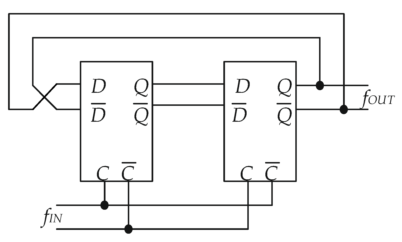
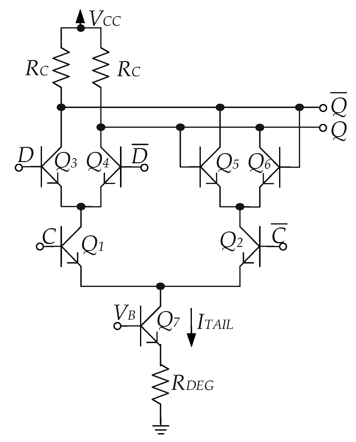
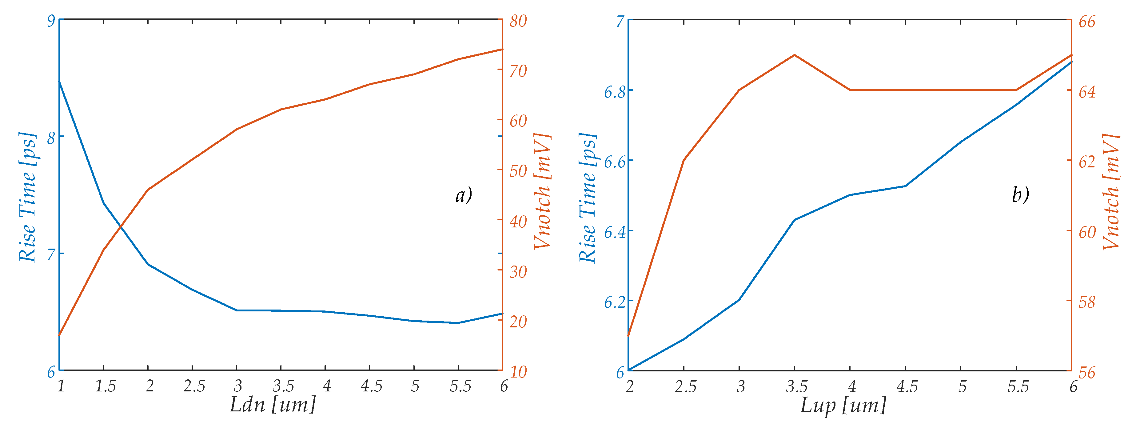
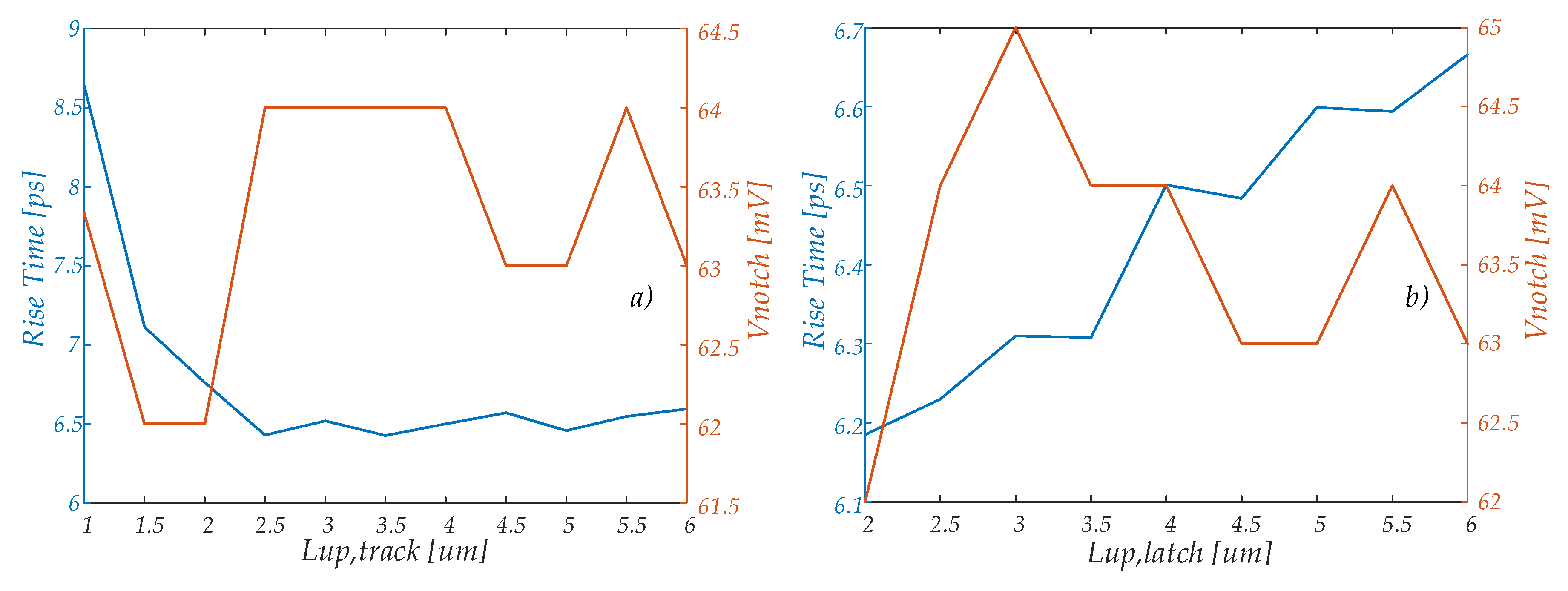
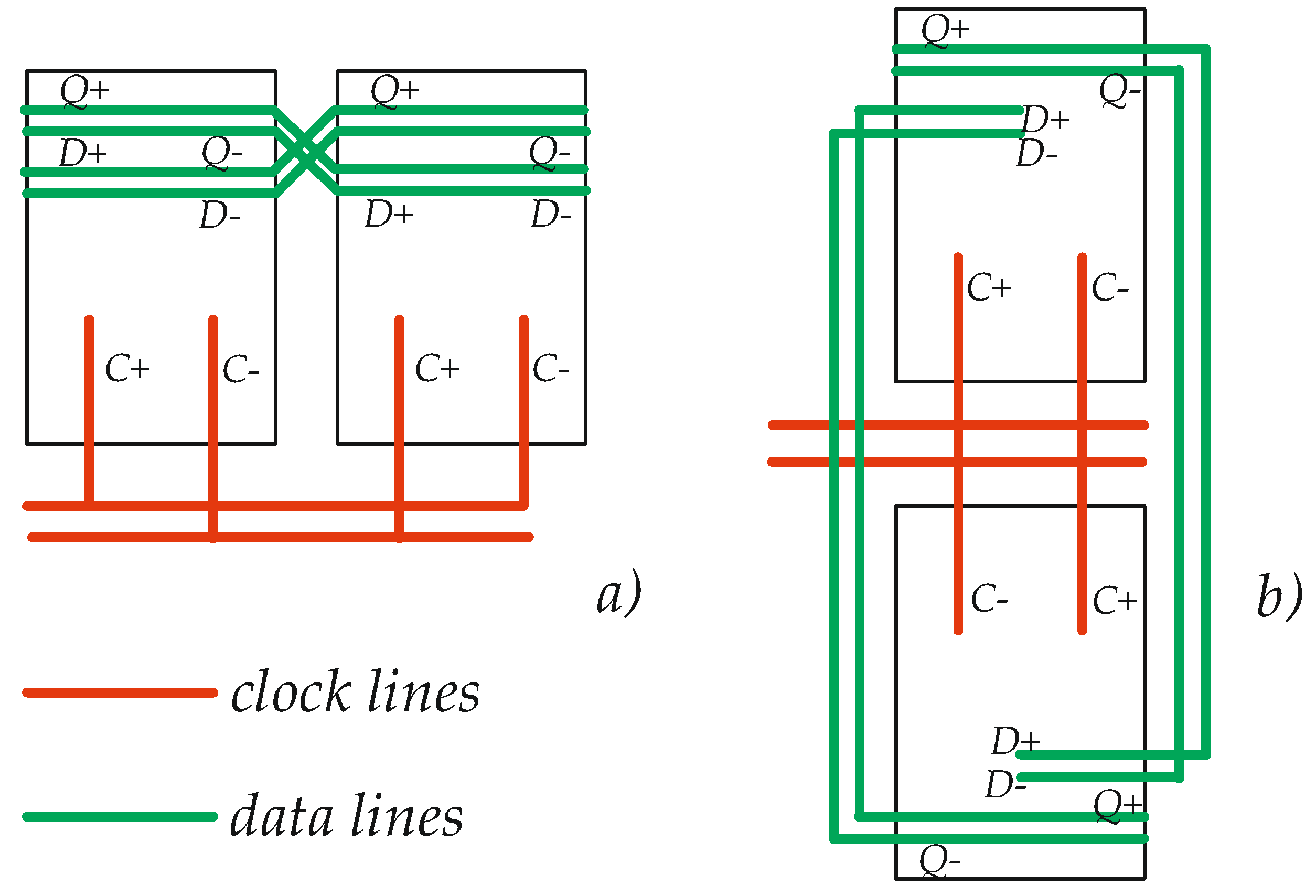
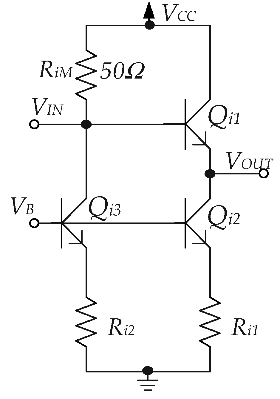
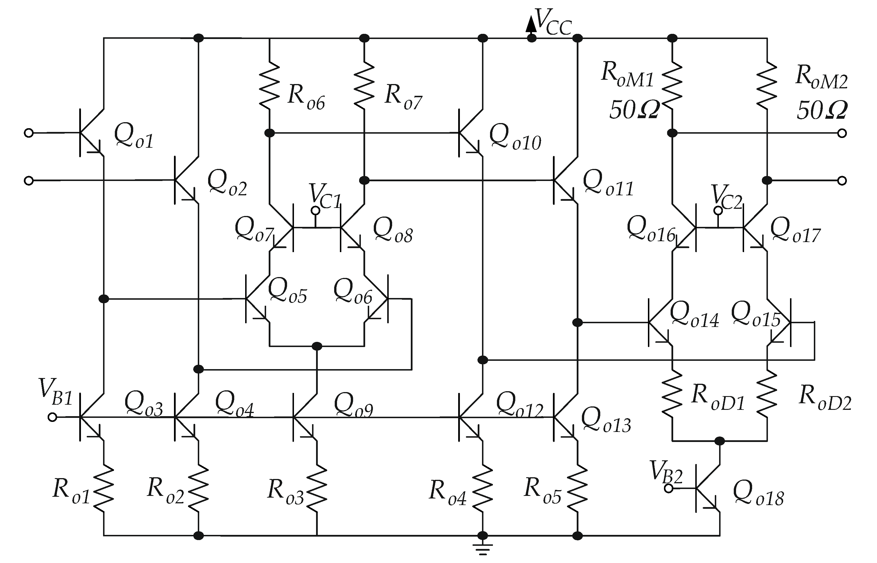
2. Frequency Divider Design

The Current Mode Logic (CML) style is based on the exclusive-OR (XOR) gate as the fundamental building block, and is often adopted for the design of SFDs operating at high frequencies. The divide-by-2 SFD is usually implemented by a CML D-type flip-flop (DFF) closed in negative feedback ( D = Q ¯ ). The CML DFF is based on a master–slave architecture in which two D-latches, driven by opposite clock signals, are cascaded, as shown in Figure 1.
Figure 2 shows the topology of a CML D-latch which is easily derived from the CML XOR gate. Inductive peaking, implemented by adding an inductor in series to the load resistors RC, is sometimes adopted to enhance the performance of the divider, and achieve higher maximum operating frequencies. However, inductors require a large silicon footprint area. This large area is not a concern for RF applications, where a sparse layout style with transmission line interconnections are used, and inductors are exploited in the different blocks for tuning and impedance matching. In mixed-signal applications, a higher integration level is usually pursued, and the minimization of silicon area occupation with a denser lumped-style layout is extremely important.
The SFD presented in this work was designed in the framework of an integrated analog front-end for 40 GS/s analog-to-digital conversion, based on the Asynchronous Time Interleaving (ATI) principle [16]. In such applications, area and power minimization are very important issues in view of a high level of integration of the whole system. To minimize the footprint area of the divider, inductive peaking was not exploited: this also allowed minimization of the length of the feedback interconnection lines (see Figure 1), which can therefore be adequately described in a lumped component approach by the RLC equivalent parasitic model.
Without inductive peaking, the speed of the divider, both in terms of SOF and of maximum frequency, which is related to the clock-to-output propagation delay [17], is mostly limited by the output time constant of the DFF. The value of this time constant is set by the value of the load resistor Rc and of the capacitances at the output node, which depend both on the sizing of the transistors of the D-latch and on the length of layout interconnections.
The divider was designed to guarantee worst-case operation at 40 GHz, and to allow some margin for testing the overall system at higher bitrates. Starting point of the design procedure was choosing the required voltage drop on the load resistor of the latch, ΔV = Rc ITAIL, which we set to 150 mV in order to fully steer the tail current in the differential pairs, with some margin to cope with voltage fluctuations due to clock feedthrough, and with process, supply voltage and temperature (PVT) variations. Clock feedthrough is a critical issue in the design of CML static frequency dividers: with reference to Figure 2, let us consider the rising edge of the clock signal C. Transistor Q1 showed an increased base current, because carriers entered the base region when the transistor exited from interdiction [18]. Moreover, the source node voltage of the pair Q1Q2 dropped when the pair was balanced, somehow reducing the tail current. All this reflects in a negative spike in the collector current, and thus in the output voltage of the D-latch, as shown in Figure 3. A too-deep spike of the output voltage could affect the behavior of the DFF and of the following blocks, in particular, when the divided output has to be used as clock signal in digital and mixed-signal applications.
Once the voltage swing was set, a careful optimization of the latch design was carried out to achieve good and robust performance at 40 GHz. The available degrees of freedom were the tail current ITAIL and size and layout of the transistors (total emitter area, and number of separate emitter areas); lower (Q1Q2) and upper (Q3Q6) levels of the D-latch were considered separately. The goals of the optimization were reliable operation of (at least) 40 GHz with sharp edges, limited clock feedthrough, low power consumption and robustness to PVT variations. An extensive set of simulations were carried out to characterize the effects of the design parameters on the output waveform of the divider, loaded by an emitter follower and a differential pair stage. The parasitic capacitive effect of interconnections, estimated in 5 fF, was also considered.
Figure 4 and Figure 5 show the dependence of the 10–90% rise time and of the voltage drop Vnotch due to the clock feedthrough (see Figure 3) on the design parameters ITAIL, Ldn and Lup, where the latter are the emitter lengths of the devices in the lower and upper differential pairs, respectively (emitter width is 0.2 μm). An ITAIL of at least 2.5 mA was needed to produce an output waveform with sharp edges, but Figure 4 also shows some dependence of the clock feedthrough on the bias current. Total emitter area determines the current density, thus the fT of the devices, but also affects the clock feedthrough [18]; these effects were particularly relevant for the lower differential pair, as shown by Figure 5a. In particular, a small emitter area minimized the notch on the output voltage, whereas sharper edges were obtained when the emitter area was increased. For the upper differential pair (Figure 5b), a minimum emitter length to current ratio of 0.5 μm/mA was required to achieve full current switching; the emitter area had little effect on the notch, but affected the rise time, because larger transistors increased the parasitic output capacitance.
We also separately considered the effect of the emitter length of devices in the track (Lup,track) and latch (Lup,latch) differential pairs, Q3–Q4 and Q5–Q6, respectively, in Figure 2. Figure 6 reports the dependence of the rise time and the notch voltage on these parameters, when ITAIL was 4 mA and all the other emitter lengths were kept constant at 4 μm. An increase in the area of the track devices improved the rise time without affecting the notch voltage, whereas increasing the latch devices slightly increased the rise time; the effect on the notch voltage was limited. Please note that the divider was not able to operate if an excessive current density was used in the latch devices (emitter length below 2 μm).
We chose to keep the emitter area low for both upper and lower devices, setting the bias current to 4 mA as a trade-off between low power consumption and a limited notch in the output waveform. Ldn was chosen to be equal to 4 μm, as a trade-off between sharp edges and a low notch, and the same value was also used for Lup to limit the current density, which would affect the full switching of the differential pairs, keeping some margin for PVT variations. Concerning the transistor layout, the output waveform was optimized when using a single emitter and single collector layout. This is justified by the fact that the capacitances both at the output nodes and at the sources of the upper level differential pair have a greater effect on the propagation delay than the parasitic base resistance, which is minimized when multiple emitter (and base) areas are used.
Degeneration resistors were added to the current mirror implementing the current source ITAIL to maximize current matching and robustness. This also increased the output resistance, minimizing variations of the current ITAIL and thus clock feedthrough.
The divider was designed and fabricated as 55 nm SiGe BiCMOS technology by STMicroelectronics [19], which offered both high speed HBT (heterojunction bipolar transistor) devices with fT/fMAX up to 320/370 GHz (high-speed devices, HS) and 1.5 V breakdown voltage and slower HBT transistors with a higher breakdown voltage (high-voltage devices, HV), together with passives (including inductors and transmission lines) and 9 levels of metals of different thickness. Table 1 synthesizes the sizing of the D-latch in Figure 2; a 3 V supply voltage was used.
The layout of the divider core (see Figure 7) was optimized to maximize the symmetry and minimize the length of the interconnection lines driven by the collectors of transistors in the latches, whose parasitic capacitance affects the output time constant and thus the divider speed. Figure 8 shows two alternative floorplans for the divider. In the floorplan of Figure 8a, the two D-latches are laid out side by side, and mirrored with respect to the vertical axis. The lines at the output of the D-latches, connecting the collectors of one D-latch, the bases of the latch pair of the same D-latch, and the bases of the track pair of the other D-latch, were fully symmetrical, their length was minimized, and any crossing with the input clock lines was avoided. The floorplan in Figure 8b, with the D-latches laid out symmetrically with respect to the horizontal axis, minimizes the length of the high frequency clock lines, but at the cost of longer output lines which cross the clock lines, thus facilitating coupling and feedthrough. Due to the compact size of the layout of each D-latch (30 × 65 μm2), the longer clock lines can still be efficiently driven by the input buffer, and we have preferred the floorplan of Figure 8a to optimize the output time constant of the D-latches and minimize clock feedthrough.

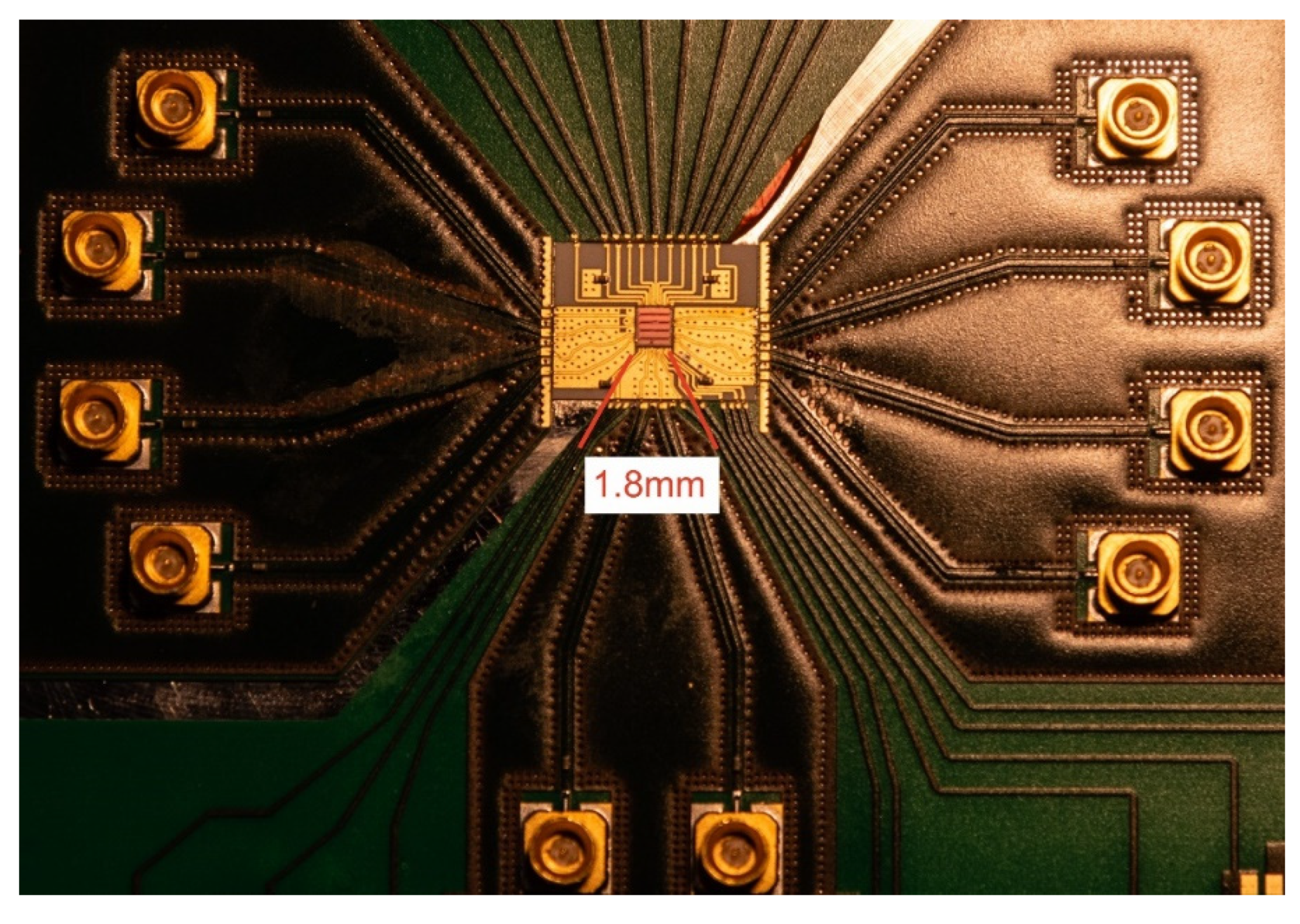
3. Design of the Divider Test Chip

The test chip included input and output buffers, to allow testing of the frequency divider block; wideband 100 Ω differential buffers were used, to allow testing of the function over a wide frequency range.
Simple emitter followers were used for the input buffer, and their bias current was optimized to drive the D-latches with the connecting lines shown in Figure 7. Between the input lines and the supply voltage, 50 Ω resistors were used for matching and biasing, as shown in Figure 9, thus allowing the use of an ac-coupled source without the need of an external biasing circuit. The common collector transistors are biased at about 2.2 mA, to provide an output resistance of about 18 Ω.
On the output side (Figure 10), the divider was followed by a limiting amplifier stage (Qo5Qo8), to achieve sharper edges and limit the effect of clock feedthrough. The limiting amplifier was driven by an emitter follower (EF) (Qo1Qo2) to minimize the loading effect and provide an adequate dc input level, and was followed by another emitter follower (Qo10Qo11) to drive the output buffer. This was designed as a degenerated cascode differential pair (Qo14Qo17), loaded by 50 Ω resistors; the degeneration resistors are sized to provide about 0 dB gain when the buffer is loaded by an (ac-coupled) 100 Ω differential load. To provide an adequate signal swing, a large dc current of more than 26 mA was used for the output buffer, thus requiring a careful design of the previous stages not to limit the bandwidth. Figure 11 shows the simulated frequency behavior of the output stage, highlighting a 3 dB bandwidth of 64 GHz.
Table 2 and Table 3 report the sizing of the transistors in the input (Figure 9) and output (Figure 10) stages, respectively. It has to be noted that the test chip was designed with separate bias references for the different blocks, to maximize testing flexibility, through the use of external potentiometers to adjust the bias currents. Figure 12 shows the layout of the frequency divider including input and output stages. The different blocks are highlighted; the divider core occupies 60 × 65 μm2, whereas the total area of divider and buffers is 190 × 400 μm2. The divider is part of a larger test chip, whose dimension are pad-limited, and differential transmission lines have been added at the input and at the output to connect the pads.

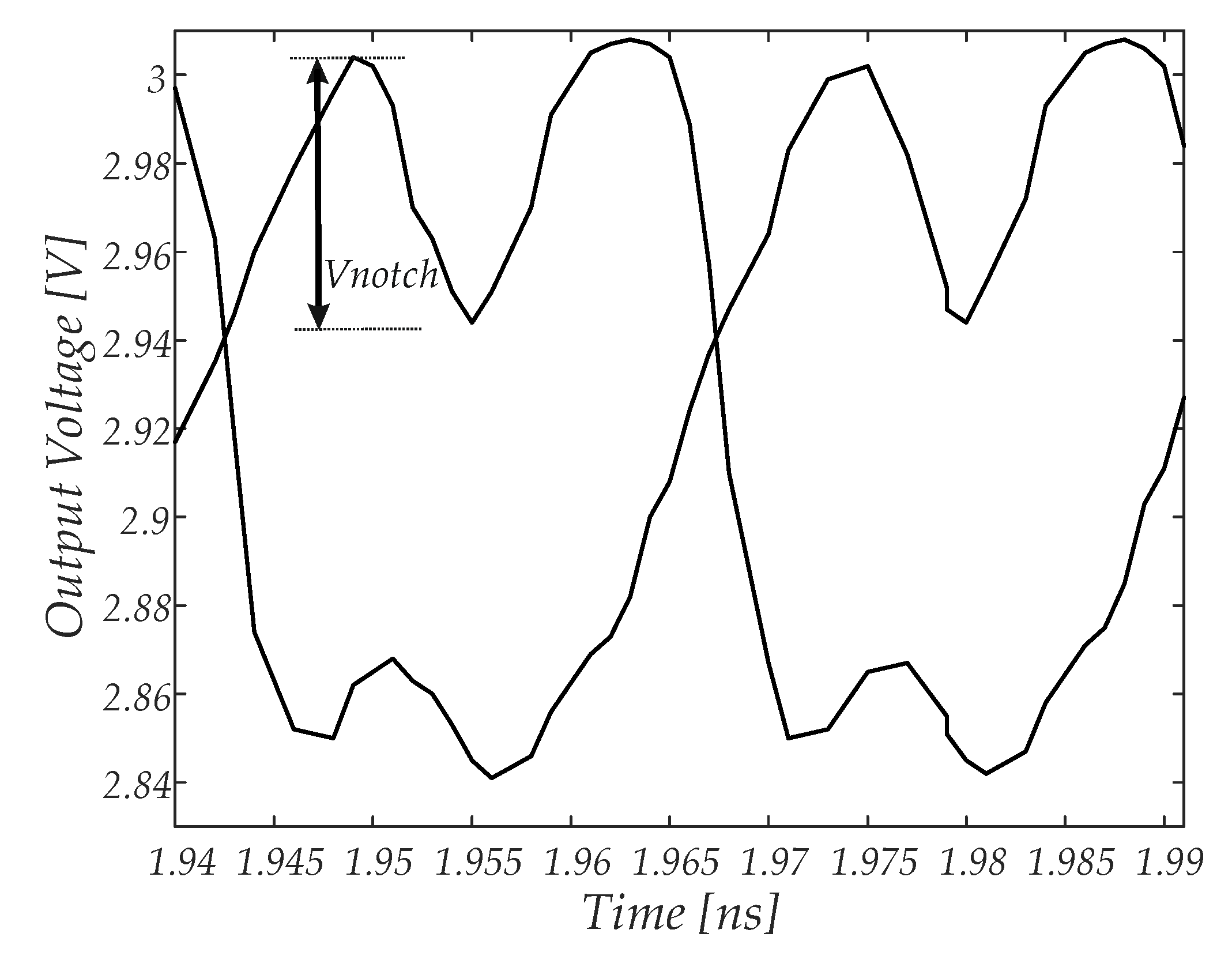
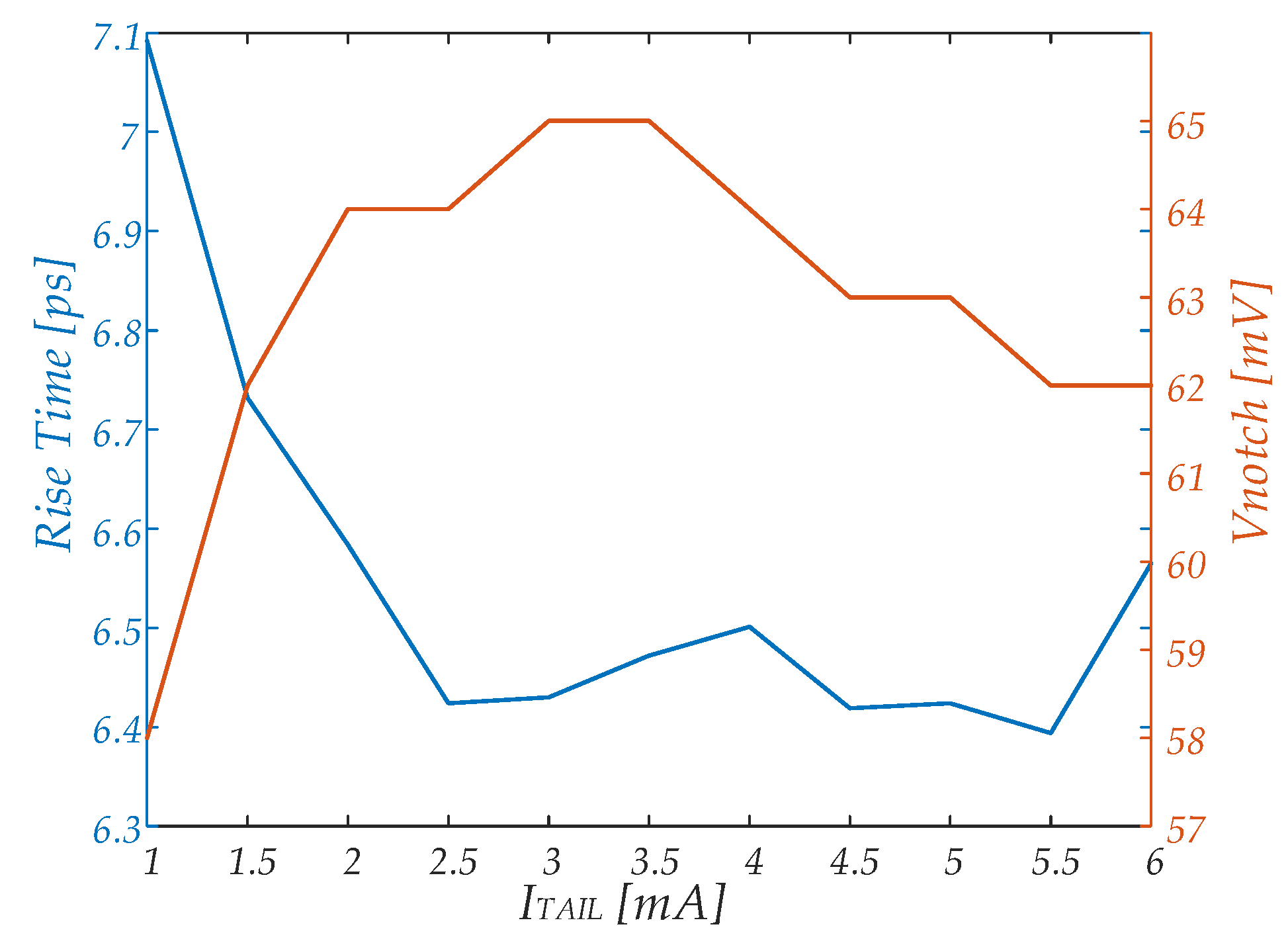
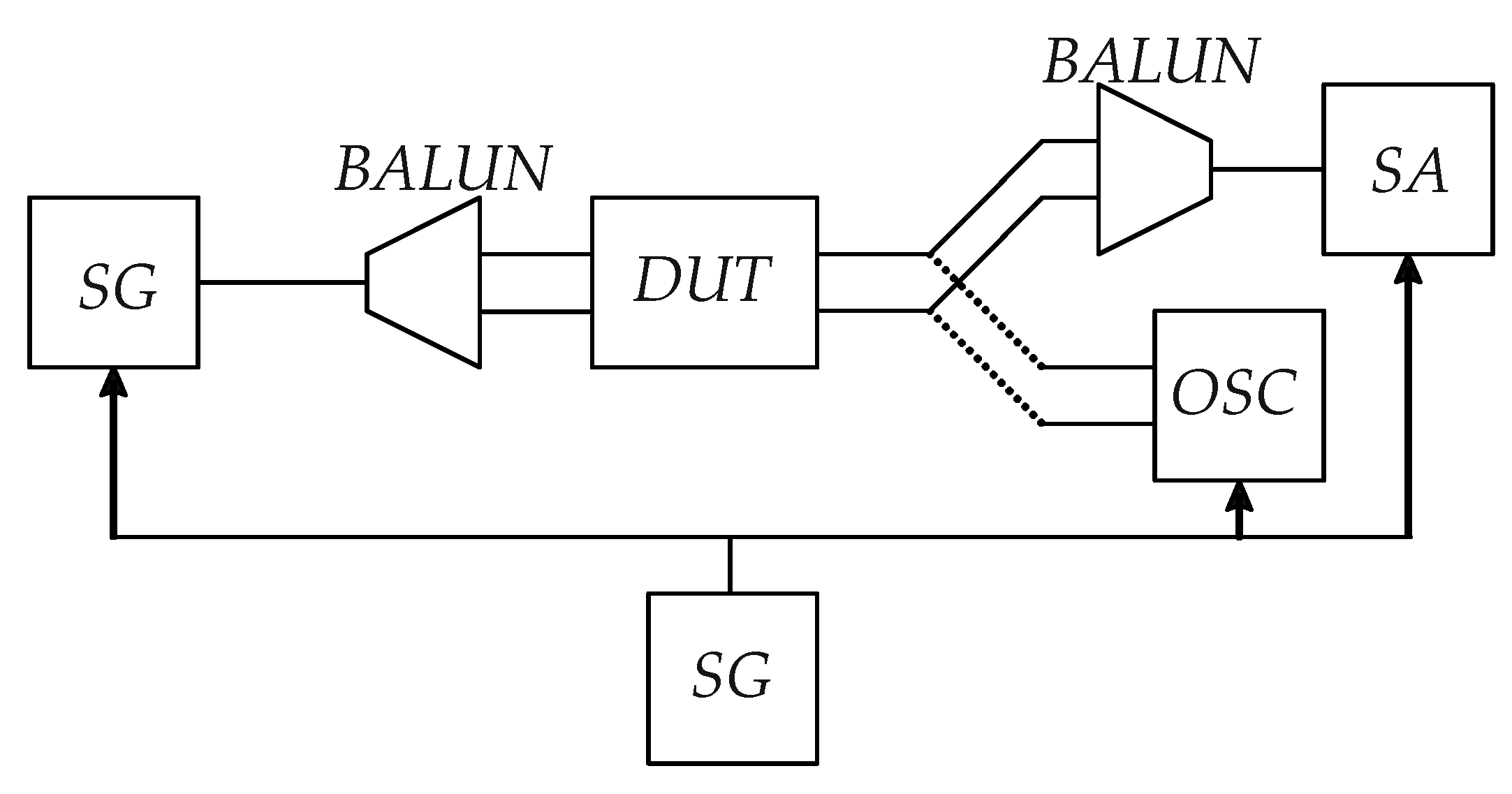
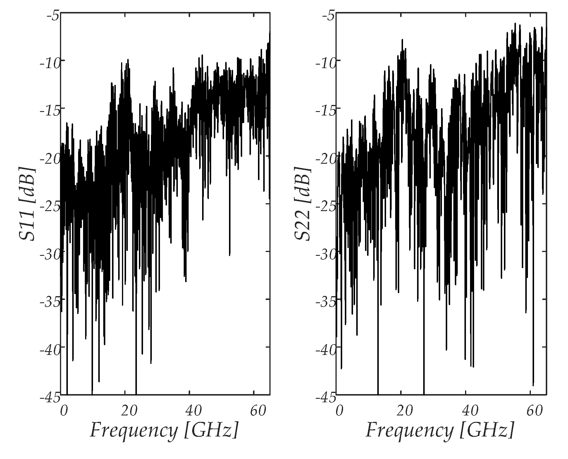
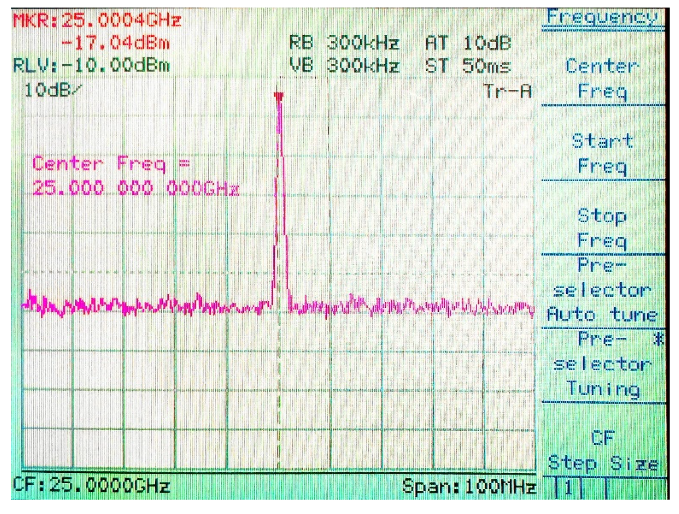
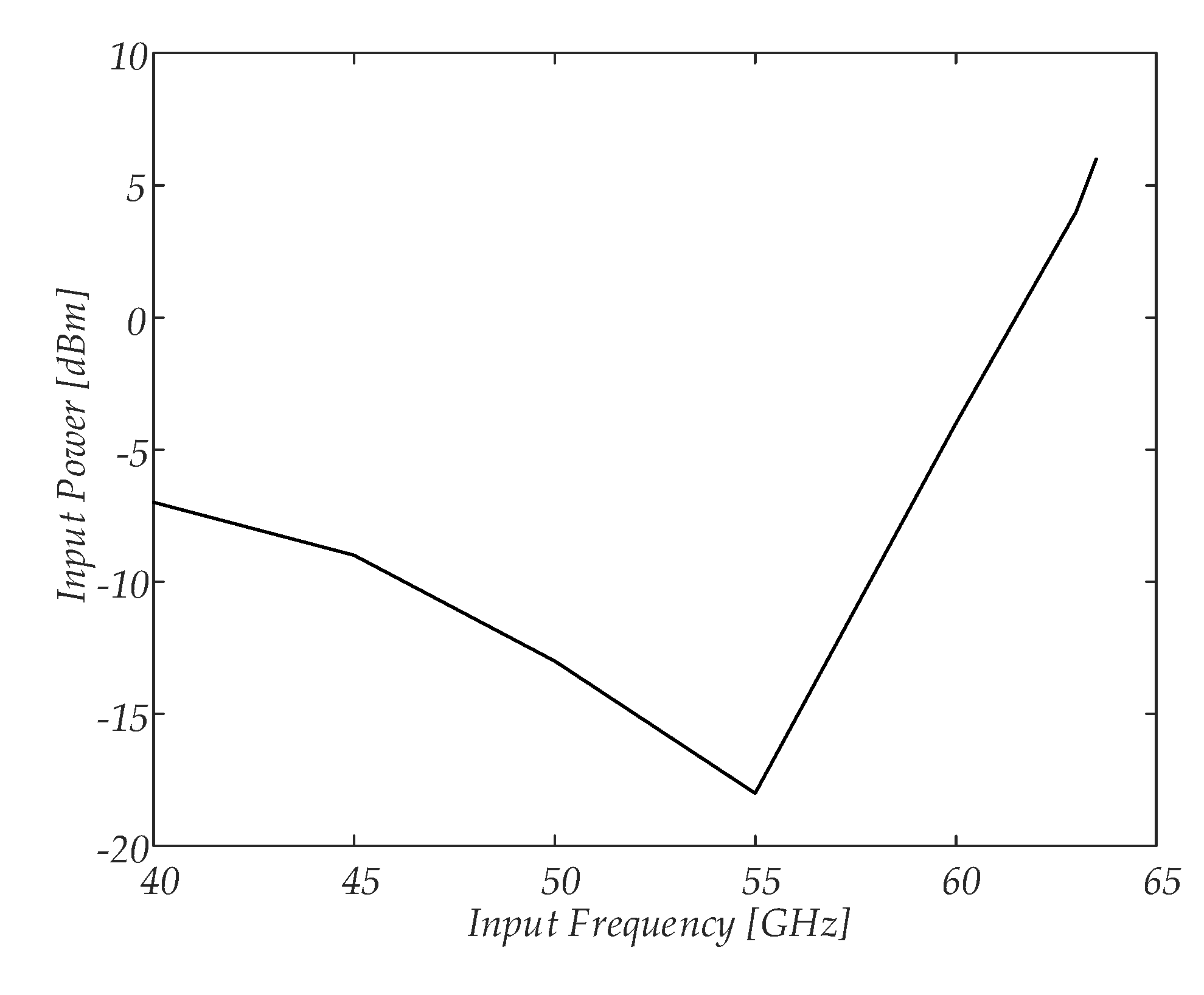
4. Measurement Results

The test chip including the frequency divider was mounted bare die on a suitable board for testing. Figure 13 shows a photograph of the test board, fabricated on a 10 mil low-loss Rogers 4350B substrate, that includes SMPM connectors, and the biasing circuitry with filtering capacitors. Grounded coplanar lines with a resistance of 50 Ω, designed by 3D EM simulations, were used for the signals, and a discontinuity in the central strip was added to solder series decoupling microwave capacitors. An alumina interposer board, which allowed thinner lines with a small pitch to be designed, was used to allow short bonding wires to connect the IC; small metal strips were used to connect the lines on the alumina and on the Rogers board. The back sides of both the alumina substrate and of the board were metalized and grounded through a metal block, used also for mechanical support.
Figure 14 schematically shows the test setup: an HP83650B signal generator with a dc-50-GHz balun or an Anritsu 69397B generator with a dc-67-GHz balun were used to generate the input signal, and the output of the divider was sent to an Anritsu MS2668C spectrum analyzer through a dc-20-GHz balun, or to a Tektronix DSA8300 digital sampling oscilloscope. The circuit drew about 75 mA from the 3 V voltage supply, which was in line with the simulations. Most of this power consumption was due to the output buffer and to the current flowing in the input 50 Ω resistors to set the input dc bias: Table 4 reports the simulated power consumption of the different blocks of the circuit, showing that the divider core dissipated about 23.7 mW.
Input and output return losses of the board were tested using an Anritsu 37397A vector network analyzer (the setup included the baluns) and are reported in Figure 15: good matching up to at least 40 GHz was achieved.
Figure 16 shows the output spectrum for a 50 GHz input signal, and Figure 17 shows the corresponding differential output waveform; the output buffer (and the output balun, when used) filtered out the output harmonics, providing a nearly sinusoidal waveform. Figure 18 shows the differential output waveform for a 20 GHz input signal, highlighting a nearly 50% duty cycle and steep edges.
The measured sensitivity curve of the divider is reported in Figure 19, and shows a maximum input frequency of 63.5 GHz and a self-oscillating frequency (SOF) of about 55 GHz, in very good agreement with post layout simulations, that provided a value of about 53.2 GHz.
Measured phase noise of −73 dBc/Hz at 1 kHz (for a 40 GHz input) appears to have been limited by the measurement setup.

5. Conclusions

The frequency divider presented in this paper was designed for a 40 GS/s application, with the goal of optimizing power and area consumption. A standard CML topology was used, without inductive peaking to avoid a large area consumption, and optimization involved mostly device sizing and biasing, and layout floor planning. Table 5 compares the results with data reported in the literature for very high frequency static frequency dividers. The ratio between the self-oscillating frequency and the power consumption of the divider core Pcore is used as a figure of merit (FOM) to evaluate the efficiency of the dividers:
FOM = SOF/Pcore,
Table 5 also specifies whether inductive peaking is used to improve frequency behavior at the cost of a larger footprint area.
The comparison shows that the proposed frequency divider provides a high efficiency, as measured by the FOM. Higher values are achieved by [24] and by dividers in CMOS technology that also exploit inductive peaking. This result shows that the proposed divider is a suitable building block to implement highly integrated, high-speed, mixed-signal systems, where minimization of footprint area and power consumption of the different building blocks is an important issue to be considered to achieve the desired level of integration.

Author Contributions

Conceptualization, F.C. and P.M.; validation, F.C., P.M. and P.T.; investigation, F.C., P.M., G.S., P.T. and A.T.; data curation, F.C., P.M. and G.S.; writing—original draft preparation, F.C., P.M., G.S. and P.T.; visualization, F.C., P.M. and G.S.; supervision, A.T.; project administration, P.T. and A.T.; funding acquisition, A.T. All authors have read and agreed to the published version of the manuscript.

Funding

This research was funded by European ECSEL-JU/EU-H2020 under grant no. 737454 TARANTO.

Acknowledgments

The authors wish to thank Markus Grözing and Philipp Thomas of Universität Stuttgart for their support in the measurement of the test chip.

Conflicts of Interest

The authors declare no conflict of interest.

References

  1. Shopov, S.; Balteanu, A.; Hasch, J.; Chevalier, P.; Cathelin, A.; Voinigescu, S.P. A 234-261-GHz 55-nm SiGe signal source with 5.4–7.2 dBm output power, 1.3% DC-to-RF efficiency, and 1-GHz divided-down output. IEEE J. Solid-State Circ. 2016, 51, 2054–2065. [Google Scholar] [CrossRef]
  2. Herzel, F.; Borngräber, J.; Ergintav, A. A 60 GHz frequency divider with quadrature outputs in 130nm SiGe BiCMOS technology for optical OFDM systems. In Proceedings of the 2015 10th European Microwave Integrated Circuits Conference (EuMIC), Paris, France, 7–8 September 2015; pp. 69–72. [Google Scholar] [CrossRef]
  3. Shu, G.; Choi, W.S.; Saxena, S.; Talegaonkar, M.; Anand, T.; Elkholy, A.; Elshazly, A.; Hanumolu, P.K. A 4-to-10.5 Gb/s continuous-rate digital clock and data recovery with automatic frequency acquisition. IEEE J. Solid-State Circ. 2016, 51, 428–439. [Google Scholar] [CrossRef]
  4. Hwang, H.; Kim, J. A 100 Gb/s quad-lane SerDes receiver with a pi-based quarter-rate all-digital CDR. Electronics 2020, 9, 1113. [Google Scholar] [CrossRef]
  5. Awny, A.; Moeller, L.; Junio, J.; Scheytt, J.C.; Thiede, A. Design and measurement techniques for an 80 Gb/s 1-tap decision feedback equalizer. IEEE J. Solid-State Circ. 2014, 49, 452–470. [Google Scholar] [CrossRef]
  6. Kull, L.; Luu, D.; Menolfi, C.; Brändli, M.; Francese, P.A.; Morf, T.; Kossel, M.; Cevrero, A.; Ozkaya, I.; Toifl, T. A 24-72-GS/s 8-b time-interleaved SAR ADC with 2.0-3.3-pJ/conversion and >30 dB SNDR at Nyquist in 14-nm CMOS FinFET. IEEE J. Solid-State Circ. 2018, 53, 3508–3516. [Google Scholar] [CrossRef]
  7. Grahn, J.V.; Fosshaug, H.; Jargelius, M.; Jönsson, P.; Linder, M.; Malm, B.G.; Mohadjeri, B.; Pejnefors, J.; Radamson, H.H.; Sandén, M.; et al. A low-complexity 62-GHz fT SiGe heterojunction bipolar transistor process using differential epitaxy and in situ phosphorus-doped poly-Si emitter at very low thermal budget. Solid-State Electron. 2000, 44, 549–554. [Google Scholar] [CrossRef]
  8. Rücker, H.; Heinemann, B. High-performance SiGe HBTs for next generation BiCMOS technology. Semicond. Sci. Technol. 2018, 33, 114003. [Google Scholar] [CrossRef]
  9. Zirath, H.; Carpenter, S.; He, Z.; Vassilev, V.; Bao, M. D-band MMIC design for high datarate wireless and wire-bound communication based on state-of-the-art InP DHBT and SiGe BiCMOS processes. In Proceedings of the 2018 Asia-Pacific Microwave Conference (APMC), Kyoto, Japan, 6–9 November 2018. [Google Scholar] [CrossRef]
  10. Voinigescu, S.P.; Shopov, S.; Hoffman, J.; Vasiliakopoulos, K. Analog and mixed-signal millimeter-wave SiGe BiCMOS circuits: State of the art and future scaling. In Proceedings of the 2016 IEEE Compound Semiconductor Integrated Circuit Symposium (CSICS), Austin, TX, USA, 23–26 October 2016. [Google Scholar] [CrossRef]
  11. Dyskin, A.; Kallfass, I. Amalytical approach for SiGe HBT static frequency divider design for millimeter-wave frequency operation. IEEE Trans. Microw. Theory Techn. 2018, 66, 1411–1417. [Google Scholar] [CrossRef]
  12. Seo, M.; Urteaga, M.; Young, A.; Rodwell, M. A 305–330+ GHz 2:1 dynamic frequency divider using InP HBTs. IEEE Microw. Wirel. Compon. Lett. 2010, 20, 468–470. [Google Scholar] [CrossRef]
  13. Lin, Y.H.; Wang, H. A 35.7–64.2 GHz low power Miller divider with weak inversion mixer in 65 nm CMOS. IEEE Microw. Wireless Compon. Lett. 2016, 26, 948–950. [Google Scholar] [CrossRef]
  14. Lin, B.-Y.; Liu, S.-I. Analysis and design of D-band injection-locked frequency dividers. IEEE J. Solid-State Circ. 2011, 46, 1250–1264. [Google Scholar] [CrossRef]
  15. Ali, U.; Bober, M.; Thiede, A.; Wagner, S. 100–166 GHz wide band high speed digital dynamic frequency divider design in 0.13 m SiGe BiCMOS technology. In Proceedings of the 2015 10th European Microwave Integrated Circuits Conference (EuMIC), Paris, France, 7–8 September 2015; pp. 73–76. [Google Scholar] [CrossRef]
  16. Monsurrò, P.; Trifiletti, A.; Angrisani, L.; D’Arco, M. Streamline calibration modelling for a comprehensive design of ATI-based digitizers. Measurement 2018, 125, 386–393. [Google Scholar] [CrossRef]
  17. Alioto, M.; Di Cataldo, G.; Palumbo, G. Design of low-power high-speed bipolar frequency dividers. Electron. Lett. 2002, 38, 158–160. [Google Scholar] [CrossRef]
  18. Schröter, M.; Rein, H.-M. Investigation of very fast and high-current transients in digital bipolar IC’s using both a new compact model and a device simulator. IEEE J. Solid-State Circ. 1995, 30, 551–562. [Google Scholar] [CrossRef]
  19. Chevalier, P.; Avenier, G.; Ribes, G.; Montagné, A.; Canderle, E.; Céli, D.; Derrier, N.; Deglise, C.; Durand, C.; Quémerais, T. A 55 nm triple gate oxide 9 metal layers SiGe BiCMOS technology featuring 320 GHz fT/370 GHz fMAX HBT and high-Q millimeter-wave passives. In Proceedings of the 2014 IEEE International Electron Devices Meeting, San Francisco, CA, USA, 15–17 December 2014; pp. 77–79. [Google Scholar] [CrossRef]
  20. Laskin, E.; Nicolson, S.T.; Chevalier, P.; Chantre, A.; Sautreuil, B.; Voinigescu, S.P. Low-power, low-phase noise SiGe HBT static frequency divider topologies up to 100 GHz. In Proceedings of the 2006 Bipolar/BiCMOS Circuits and Technology Meeting, Maastricht, The Netherlands, 8–10 October 2006. [Google Scholar] [CrossRef]
  21. Voinigescu, S.P.; Aroca, R.; Dickson, T.O.; Nicolson, S.T.; Chalvatzis, T.; Chevalier, P.; Garcia, P.; Garnier, C.; Sautreuil, B. Towards a sub-2.5V, 100-Gb/s serial transceiver. In Proceedings of the 2007 IEEE Custom Integrated Circuits Conference, San Jose, CA, USA, 16–19 September 2007; pp. 471–478. [Google Scholar] [CrossRef]
  22. Trotta, S.; Li, H.; Trivedi, V.P.; John, J. A tunable flipflop-based frequency divider up to 113 GHz and a fully differential 77GHz push-push VCO in SiGe BiCMOS technology. In Proceedings of the 2009 IEEE Radio Frequency Integrated Circuits Symposium, Boston, MA, USA, 7–9 June 2009; pp. 47–50. [Google Scholar] [CrossRef]
  23. D’Amore, M.; Monier, C.; Lin, S.; Oyama, B.; Scott, D.; Kaneshiro, E.; Gutierrez-Aitken, A.; Oki, A. A 0.25μm InP DHBT 200GHz+ static frequency divider. In Proceedings of the CSICS 2009 IEEE Compound Semiconductor Integrated Circuit Symposium, Greensboro, NC, USA, 11–14 October 2009. [Google Scholar] [CrossRef]
  24. Knapp, H.; Meister, T.F.; Liebl, W.; Claeys, D.; Popp, T.; Aufinger, K.; Schäfer, H.; Böck, J.; Boguth, S.; Lachner, R. Static frequency dividers up to 133 GHz in SiGe:C bipolar technology. In Proceedings of the 2010 IEEE Bipolar/BiCMOS Circuits and Technology Meeting (BCTM), Austin, TX, USA, 4–6 October 2010; pp. 29–32. [Google Scholar] [CrossRef]
  25. Ali, U.; Bober, M.; Thiede, A.; Awny, A.; Fischer, G. High speed static frequency divider design with 111.6 GHz self-oscillation frequency (SOF) in 0.13 m SiGe BiCMOS technology. In Proceedings of the 2015 German Microwave Conference, Nuremberg, Germany, 16–18 March 2015; pp. 241–243. [Google Scholar] [CrossRef]
  26. Dyskin, A.; Harati, P.; Kallfass, I. Layout and interconnect optimization for low-power and high-sensitivity operation of E-band SiGe HBT frequency dividers. IEEE Microw. Wirel. Compon. Lett. 2018, 28, 67–69. [Google Scholar] [CrossRef]
  27. Rehman, S.U.; Ferchichi, A.; Khafaji, M.M.; Carta, C.; Ellinger, F. A 1–60 GHz 9.6 mW 0.18 V output-swing static clock divider circuit in 45-nm SOI CMOS. In Proceedings of the 2018 25th IEEE International Conference on Electronics, Bordeaux, France, 9–12 December 2018; pp. 41–44. [Google Scholar] [CrossRef]
  28. Zhou, P.; Chen, J.; Yan, P.; Hou, D.; Hong, W. A low power, high sensitivity SiGe HBT static frequency divider up to 90 GHz for millimeter-wave application. China Commun. 2019, 16, 85–94. [Google Scholar]
Figure 1. Block scheme of a Current Mode Logic (CML) static frequency divider.
Electronics 09 01968 g001
Figure 2. CML D-latch schematic.
Electronics 09 01968 g002
Figure 3. Output waveforms of the divider.
Electronics 09 01968 g003
Figure 4. Dependence of rise time and notch voltage on the tail current of the latch.
Electronics 09 01968 g004
Figure 5. Dependence of rise time and notch voltage on the emitter length of (a) devices of the lower differential pair; and (b) devices of the upper differential pair. ITAIL was 4 mA and the emitter length for the other devices was 4 μm.
Electronics 09 01968 g005
Figure 6. Dependence of rise time and notch voltage on the emitter length of the upper devices, considering separately (a) the track differential pair; and (b) the latch differential pair. ITAIL was 4 mA and the emitter length for the other devices was 4 μm.
Electronics 09 01968 g006
Figure 7. Layout of the divider core.
Electronics 09 01968 g007
Figure 8. Floorplan of the D-type flip-flop (DFF): (a) D-latches flipped around the vertical axis; (b) D-latches flipped around the horizontal axis.
Electronics 09 01968 g008
Figure 9. Schematic of the input buffer.
Electronics 09 01968 g009
Figure 10. Schematic of the output buffer.
Electronics 09 01968 g010
Figure 11. Simulated transfer function of the output stage.
Electronics 09 01968 g011
Figure 12. Layout of the full divider with input and output stages.
Electronics 09 01968 g012
Figure 13. Photograph of the test board. The size of the test chip was 1.8 × 1.98 mm2.
Electronics 09 01968 g013
Figure 14. Block scheme of the test setup.
Electronics 09 01968 g014
Figure 15. Measured input and output return losses.
Electronics 09 01968 g015
Figure 16. Output spectrum for a 50 GHz input.
Electronics 09 01968 g016
Figure 17. Differential output waveform for a 50 GHz input.
Electronics 09 01968 g017
Figure 18. Differential output waveform for a 20 GHz input.
Electronics 09 01968 g018
Figure 19. Measured sensitivity curve of the frequency divider.
Electronics 09 01968 g019
Table 1. Dimensions of transistors of the D-latch.
TransistorTotal Emitter Area (μm2)HBT Type and Number of Emitters
Q1, Q20.8HS, 1 emitter
Q3, Q4, Q5, Q60.8HS, 1 emitter
Q73.2HS, 2 emitters
ResistorValue-
RC37.5 Ω-
Rdeg50 Ω-
Table 2. Dimensions of transistors of the input stage.
TransistorTotal Emitter Area (μm2)HBT Type and Number of Emitters
Qi11.6HS, 2 emitters
Qi2, Qi31.6HV, 2 emitters
ResistorValue-
RiM50 Ω-
Ri1, Ri2100 Ω-
Table 3. Dimensions of transistors of the output stage.
TransistorTotal Emitter Area (μm2)HBT Type and Number of Emitters
Qo1, Qo20.4HS, 1 emitter
Qo3, Qo41.6HS, 2 emitters
Qo5, Qo61.2HS, 2 emitters
Qo7, Qo80,6HS, 1 emitter
Qo91.6HS, 2 emitters
Qo10, Qo111.6HS, 2 emitters
Qo12, Qo131.6HS, 2 emitters
Qo14, Qo154HS, 4 emitters
Qo16, Qo172HS, 4 emitters
Qo188.4HS, 8 emitters
ResistorValue-
Ro1, Ro2, Ro3100 Ω-
Ro6, Ro7100 Ω-
Ro4, Ro5100 Ω-
RoM1, RoM250 Ω-
RoD1, RoD221.5 Ω-
Table 4. Break-down of power consumption of the frequency divider.
BlockPower Consumption
Input Buffer26.8 mW
Divider Core23.7 mW
Limiter with EFs28.9 mW
Output Buffer78.6 mW
Biasing51.9 mW
Table 5. Comparison with the literature.
ReferenceTechnology (fT)InductorSOFfmaxPcoreFOM
[20]SiGe (230)Y771001220.63
[21]CMOS 65 nmY79.29019.24.12
[21]SiGe (150)Y92104561.64
[22]SiGe (200)N1041131150.90
[23]InP (530)Y1732002280.76
[24]SiGe (230)N5687144.00
[24]SiGe (230)N961332100.46
[5]SiGe (240)N70.31001410.50
[25]SiGe (300)No111.6128.71960.57
[2]SiGe (240)Y52601150.45
[26]SiGe (250)N7780800.96
[27]CMOS 45 nmY60609.66.25
[28]SiGe (200)Y75.19061.61.22
This WorkSiGe (320)N5563.523.72.32
-(GHz)-GHzGHzmWGHz/mW
Publisher’s Note: MDPI stays neutral with regard to jurisdictional claims in published maps and institutional affiliations.

