Abstract
The design of single-stage OTAs for accurate switched-capacitor circuits involves challenging trade-offs between speed and power consumption. The addition of a Slew-Rate Enhancer (SRE) circuit placed in parallel to the main OTA (parallel-type SRE) constitutes a viable solution to reduce the settling time, at the cost of low-power overhead and no modifications of the main OTA. In this work, a practical analytical model has been developed to predict the settling time reduction achievable with OTA/SRE systems and to show the effect of the various design parameters. The model has been applied to a real case, consisting of the combination of a standard folded-cascode OTA with an existing parallel-type SRE solution. Simulations performed on a circuit designed with a commercial 180-nm CMOS technology revealed that the actual settling-time reduction was significantly smaller than predicted by the model. This discrepancy was explained by taking into account the internal delays of the SRE, which is exacerbated when a high output current gain is combined with high power efficiency. To overcome this problem, we propose a simple modification of the original SRE circuit, consisting in the addition of a single capacitor which temporarily boosts the OTA/SRE currents reducing the internal turn-on delay. With the proposed approach a settling-time reduction of 57% has been demonstrated with an SRE that introduces only a 10% power-overhead with respect of the single OTA solution. The robustness of the results have been validated by means of Monte-Carlo simulations.
1. Introduction
Switched-capacitors (SC) circuits are commonly used in mixed-signal ICs to process data related to sensors and actuators including filters, analog-to-digital and digital-to-analog converters. The IoT paradigm, with its many expressions, imposes extremely low power consumption to such blocks, pushing the boundaries of the design techniques. Slew-rate (SR) enhancement techniques tackle power consumption reduction in SC circuits, since they can be employed to shorten the settling times of the commutation transients and to assist the charge transfer without raising the internal bias currents of the active blocks. SC circuits are the common implementation of sampled-data signal processing techniques, where the signal needs to correctly settle at the end of the sampling phase, regardless on its previous transient evolution. For this reason, circuital solutions that allow for much higher output currents than the quiescent current absorption (such as class-AB stages) can be applied to SC circuits with more relaxed distortion constraints than to their continuous time counterparts, whose output signals need to be valid during all the transient evolution. In addition, the absence of resistive loading favours the use of single stage OTAs in most SC architectures. This reflects into the large amount of works dedicated to new single-stage OTAs for SC applications, optimized for power vs. speed trade-off, which can be classified into four major categories:
- Class-AB input pairs employ input devices with a variable bias current which allows for dynamic increase of both OTA transconductance and current capacity following large voltage steps. Class-AB input pairs can be implemented by dynamically controlling the tail current injected into the common source of the input differential pair, or by topological modifications of the input pair based on the flipped-voltage follower [1]. Different strategies have been proposed: (i) charge release synchronized with clock phases [2], (ii) current boosting by sensing input voltage steps [3,4,5,6,7] or (iii) at other OTA’s internal nodes [8,9,10]. However, large impulsive currents in the internal branches do not contribute directly to the current delivered to the output capacitive load and, consequently, represent wasted power; furthermore, the upset caused by large increases of the internal currents may result in a settling penalty due to saturation of sensitive devices [11] or it may even cause trojan states [12].
- Non-linear current steering: this category comprises many families of single-stage OTA topologies that differ about the specific current operations performed by the network that conveys the currents of the input devices to the output port. Generally, all the topologies falling in this category aim to achieve class-AB action on the output branches maintaining the simplicity of the differential pair in the input section. This can be implemented through: (i) non-linear current mirrors [13,14,15,16,17], (ii) transconductor nesting [18,19] or (iii) current recycling [20,21,22,23,24,25,26,27,28,29]. The important feature of such implementations is that the increased output current capability does not involve an increased dc supply power, in contrast with what happens with a static current amplification approach. However, in many of these implementations, the appearance of non-dominant internal singularities makes the optimization difficult for small-to-medium capacitive loads due to phase margin degradation [30].
- RC-tie [31] or quasi-floating gate [32,33] configurations for OTA output branches efficiently provide class-AB action directly on the OTA output branches. They are implemented through a decoupling capacitor across the gates of the respective p-type and n-type transistors statically charged to maintain an adequate bias current through the stacked output devices. Any ac signal coupled to either the NMOS or the PMOS will be transferred to the stack in a push-pull fashion. Globally, the OTA presents a band-pass open loop characteristic which can be tuned to cover the range of frequency of interest.
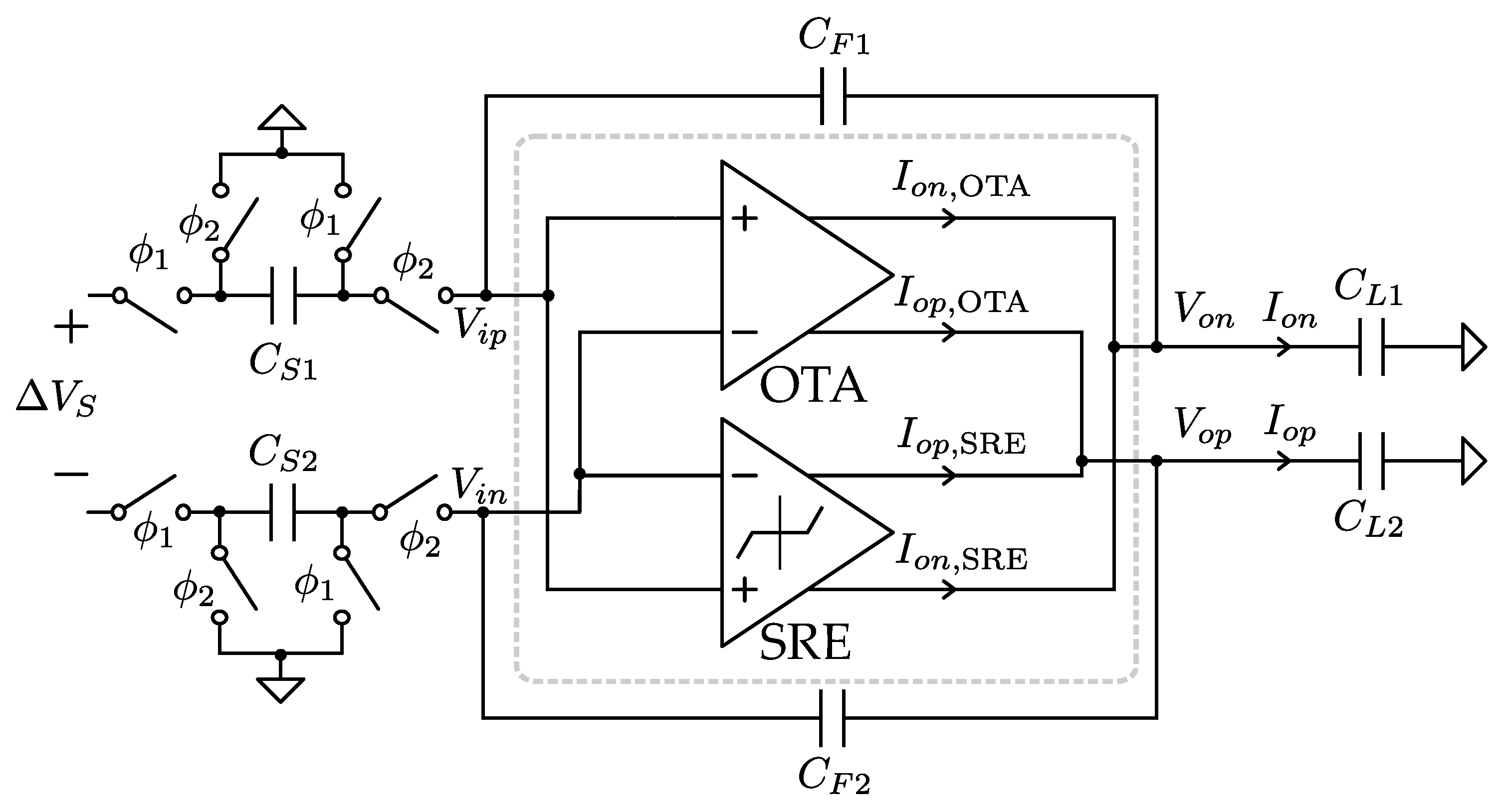
- An auxiliary OTA structure or part of it can be used as slew-rate enhancer (SRE) which aims to add an extra current directly to the output load in parallel with the main OTA current path. In order to achieve low power operation, the auxiliary circuit automatically turns off once the current needed by the load is small. This is fundamental in single-stage architectures where the main OTA provides gain through its high-impedance output nodes. Any gain loss due to the presence of parallel branches in the output nodes would cause precision loss at the end of the operation time. This can be avoided by forcing the cut-off state of the auxiliary SRE. This technique is of general use and can be extended also to multi-stage OTA configurations [34,35]. Auxiliary SRE implementations contemplate main-OTA internal-node sensing [36,37,38,39,40,41], or direct sensing of the OTA inputs (parallel-type SRE) [42,43,44]. In the latter case, a complete OTA/SRE system is used as shown in Figure 1. A totally passive, OTA-free SRE technique has been recently proposed for modulators [45].
Figure 1. Example of SC integrator based on single-stage OTA and parallel-type SRE.
The aforementioned classification is provided as a general guide for working principles in advanced single-stage OTAs, although many of the cited works use combined techniques to achieve superior performance in terms of slew-rate (SR), gain-bandwidth product (GBW) and static gain, as can be found in the super class-AB topologies [14,15,26,27,28]. Still, few efforts were made to emphasize and contextualize the auxiliary parallel-type SREs with clear design guidelines. This work focuses on parallel-type auxiliary SRE, based on the pioneering works of Nagaraj [42,43], which, as will be discussed later, allows for decoupled specifications and optimization with respect to the main OTA. The principle of parallel-type SRE is illustrated in Figure 1, showing an OTA/SRE combination used as a power-efficient gain stage for a switched capacitor, fully differential integrator.
In this work, a practical settling time model is presented, useful for the design of OTA-SC circuits, including SC amplifiers, SC integrators and SC resonators, which find extensive applications in filters, capacitive-load drivers, and pipeline ADCs. The extension of this model to SREs, and in particular to Nagaraj’s SRE [42], clarifies essential conditions and trade-offs to make SREs attractive solutions to speed-up the circuit settling. Moreover, an improved version of the original Nagaraj’s SRE is presented, which exploits a capacitive boosting to reduce the SRE internal delays and maximize its effectiveness.
The remainder of this paper is organized as follows: Section 2 describes the aforementioned analytical settling time model, which, for its generality, can be applied to any single stage amplifiers regardless of the presence of output current boosting mechanisms; Section 3 describes the application of the model to a particular case of an OTA/SRE combination and compares the prediction of the model with simulated results obtained from the combination of a standard folded cascode OTA and the Nagaraj’s SRE. In the same section, the improved SRE circuit is described and the achievable advantages are demonstrated by means of simulations. Finally, conclusions are drawn in Section 4.
2. OTA-Assisted Charge Transfer Process
2.1. The Switched-Capacitors Stage
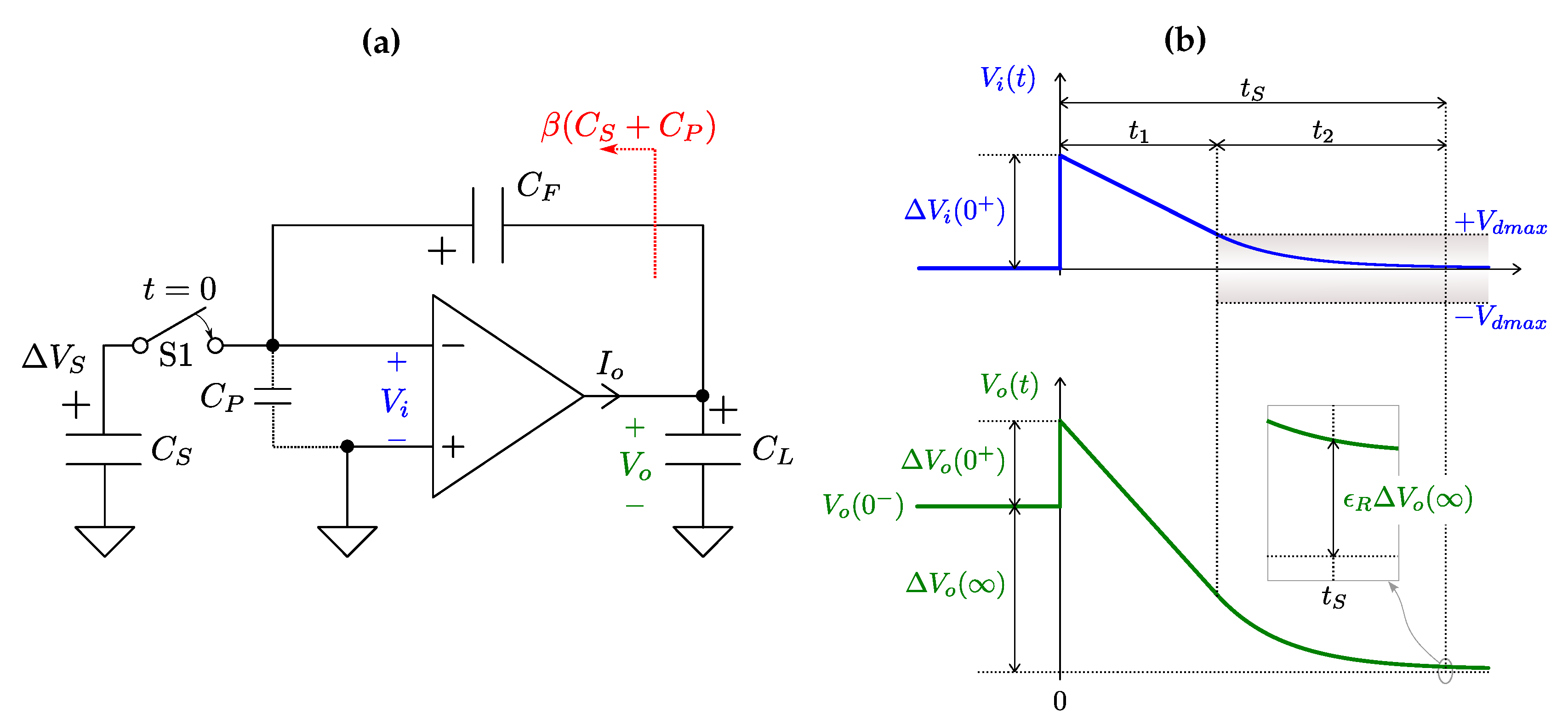
Accurate SC circuits are generally implemented using fully differential architectures such that of Figure 1. Nevertheless, it is convenient to represent the behaviour of fully differential circuit using a single-ended equivalent circuit such that of Figure 2a. Voltages and currents of the single-ended model represent the total differential mode components of the original fully differential circuit. It can be easily shown that the only transformation that have to be applied regards the input capacitance of the OTA in the equivalent circuit, in Figure 2a, which should be set to twice the input capacitance of the fully differential OTA. Considering Figure 1, the other capacitances of the circuit are simply replicated in the single-ended equivalent, i.e., , , .
Figure 2.
Charge transfer model in a SC stage (a) and its relevant voltage waveforms (b).
The circuit represented in Figure 2a models the charge transfer operation from capacitor , where the input signal is initially stored in form of a charge sample , to the OTA feedback capacitor . The presence of a following stage is here modeled through a capacitive load . This represents exactly what happens in the circuit of Figure 2, once the mentioned fully differential to single-ended transformation is considered.
Nevertheless, it can be easily shown that the circuit in Figure 2a provides an exact representation of many other frequently used switching strategies, such as the case where one terminal of is fixed to the OTA input and the other terminal is swept across two sources with a voltage difference of [46,47]. Furthermore, as far as the voltages across capacitor are concerned, we are interested only in the variation caused by the input transition (switch S1), independently on whether these capacitors are discharged or not before S1 transition; hence the following analysis is applicable to both SC amplifiers [47] and integrators [48].
Since we are focused on the settling time, in the following discussion we will neglect the OTA finite-gain effects, considering the gain to be high enough to guarantee a perfect virtual ground across the OTA’s input terminals in stationary conditions. For the same reason, offset and input referred noise will not be considered here. Therefore, we will assume that the input voltage of the OTA will asymptotically tend to zero after any transient.
At the instant , the charge initially present on is discharged into the amplifier inverting input. In the first place, the inertia against voltage changes of the capacitors’ net causes to step in the opposite direction with respect to the desired final value. Neglecting any series resistance in the switches and interconnections, the OTA output and input are instantaneously displaced as shown in Figure 2b by:
where the feedback coefficient, , the equivalent input-referred capacitance, and the input attenuation are defined as
Asymptotically, the output voltage increment, , tends to:
The fact that is independent from the values of and is simply a consequence of assuming a perfect virtual ground in stationary conditions (asymptotic virtual ground).
In practical cases, the output voltage is sampled after a finite time, thus the actual output variations will present an error with respect to the ideal value. Defining the relative error as follows:
we are interested in the minimum settling time required to guarantee that is equal or smaller than a target value. Since both and are usually given as specifications, the designer asserts Equation (4) by proper choice of OTA topology, devices geometrical features and current consumption.
2.2. Simplified Model of Charge Transfer Transient
We will now consider that the very fast (ideally instantaneous) input and output transitions described by Equation (1) are completed. From this instant on, the system evolves towards the asymptotic value according to the following equations:
where is the total load capacitance given by:
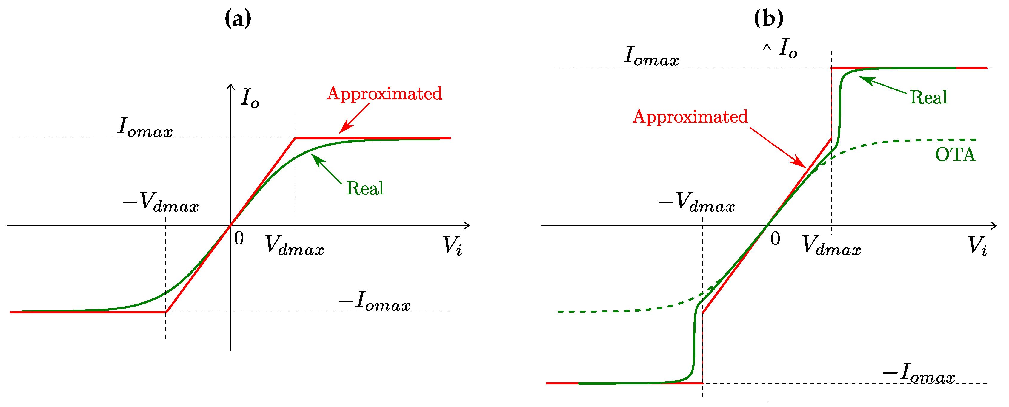
In this section, we model the saturation of the OTA current using the following piece-wise linear approximation, which considers a linear relationship between the output current and the input voltage for values of the latter up to a magnitude and a constant current of magnitude for input voltages that exceed , i.e., when the OTA is in slew-rate (SR) regime:
where is the OTA transconductance in the linear region.
For the sake of clarity, we just recall here that is equal to the differential output current of the original fully differential circuit, i.e., in Figure 1. The application of the piece-wise linear approximation to the characteristic of a class-A OTA is shown in Figure 3a. In this case, the output current is simply proportional to the differential current of the input pair and it is convenient to set to the OTA small signal transconductance and to , avoiding discontinuities in the transfer characteristic [49]. On the other hand, class-AB stages such as the OTA/SRE combination of Figure 1 can be modelled with the discontinuous characteristic of Figure 3b, where .
Figure 3.
Piece-wise linear representation of the OTA transfer characteristic for a conventional class-A stage (a) and for an OTA/SRE combination (b).
In this work, we are interested in all the cases where the slew-rate phenomenon strongly affects the settling time, thus we will consider only input stimuli as large as to bring the OTA input voltage out of the linearity region at . This occurs when , given by Equation (1), exceeds . The occurrence of such large input stimuli is frequent in many SC circuits and should be regarded as a worst case when determining the settling time. In these conditions the amplifier starts the transient in slew-rate and remains in this non-linear condition for a period (SR time), ending when gets smaller than . After the slew period, the amplifiers enter linear region where the voltage evolution is exponential. This simplified view is represented in Figure 2b. The settling time is then given by the sum:
where is the period of time spent in the linear response region until the relative error defined by Equation (4) gets and remains smaller than the target value.
Initially () the OTA responds with its maximum output current, . As a consequence both and are bounded to slew linearly with a slope fixed by . From Equations (5) and (7), it can be shown that the OTA’s input slews at a rate . This situation persists until reaches . From Equation (5) and the initial condition on the input voltage given in (1), the SR time can be calculated as
Notice that in the rightmost hand of Equation (9) we have introduced a factor defined as:
where is the total supply current of the OTA. This coefficient represents a sort of current efficiency of the given amplifier topology and is generally smaller than one in pure class-A architectures. Section 3 will discuss for OTA/SRE systems.
For , the OTA input voltage gets smaller than and, according to the approximation given by Equation (7), the output current starts being proportional to the input voltage through the overall transconductance . We will also assume that the open-loop frequency response of the amplifier is dominated by the pole associated to the output port. In these conditions, it can be easily shown that the linear transient is a simple exponential decay characterized by the time constant:
where is the 0-dB frequency of circuit loop-gain. Then, the linear time will be simply given by:
where is the value assumed by the input voltage when has settled to the final asymptotic value with a margin equal or smaller than the target relative error . From Equations (3)–(5), turns out to be:
Using the values found so far for the SR time and the linear time , we can now calculate the total settling time given by:
This expression can be simplified by considering that the ratio has the dimensions of voltage, so that we can express it as a function of by defining the dimensionless factor as:
The maximum input voltage generally depends on the input devices of the OTA, while the overall is proportional to the transconductance of the input devices () through a factor defined as:
Using Equation (15), the expression of the settling time can be finally written as:
where the expression has been made more compact by introducing time and coefficient , defined as:
Equation (17) is applicable if the following conditions are verified: and , which correspond respectively to a transient starting in SR regime and ending in the linear region when the settling time is reached. The apparent complexity of expressions in Equation (17) can be clarified by identifying the various parameters:
- , : both parameters descend from system-level specifications. The former contains: (i) which is strictly related to (see Equation (2)) and thus to kT/C-noise specifications, (ii) , which is the maximum stimulus that can be applied to the circuit (may approach the supply voltage in SC ADCs) and (iii) , which is determined by the power budget. On the other hand, can be related to precision, linearity and maximum tolerable harmonic distortion, depending on the application of the SC amplifier/integrator.
- and : both parameters mainly depend on the capacitive feedback network (, ) and on the load . The ratio is determined at system level to achieve the desired gain or integrator coefficient, through Equation (3). The contribution of the input capacitance to the coefficients and may be significant when input devices with large gate area are chosen to minimize the offset voltage and the flicker noise and/or particularly small values are chosen for , and to enable fast clock frequencies.
- and express the efficiency by which the OTA uses the given supply current to produce large output currents and large transconductances, respectively.
- is composed by a specification (), dictated by the application, and by , which is a real degree of freedom that characterizes the design of the OTA.
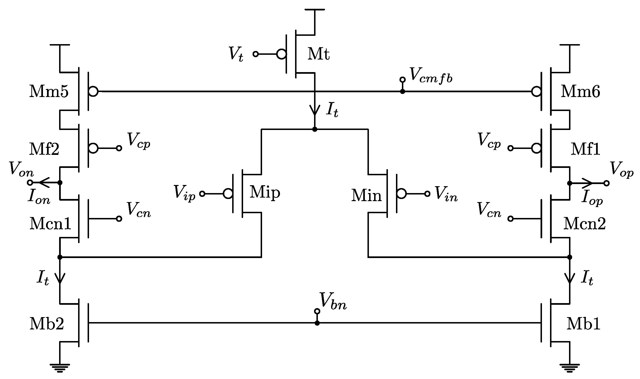
In next section, the Nagaraj’s SRE will be applied to the standard folded cascode (FC) OTA shown in Figure 4. The FC OTA is still widely used in SC circuits for its high gain, high speed and circuital simplicity. We will consider the typical bias current distribution shown in the figure, where the common source stage (Mip, Min) and the common gate one (Mcn1, Mcn2) are both biased by the same current . This choice results in: . Using for this stage the approximation shown in Figure 3a and considering definition (15), we find . For the topology in Figure 4, we have studied the effect of on the settling time. For this test, we have assumed a case study with pF, pF, pF and pF, resulting in the following values for the capacitance ratios , and .
Figure 4.
Fully differential FC OTA schematic. .
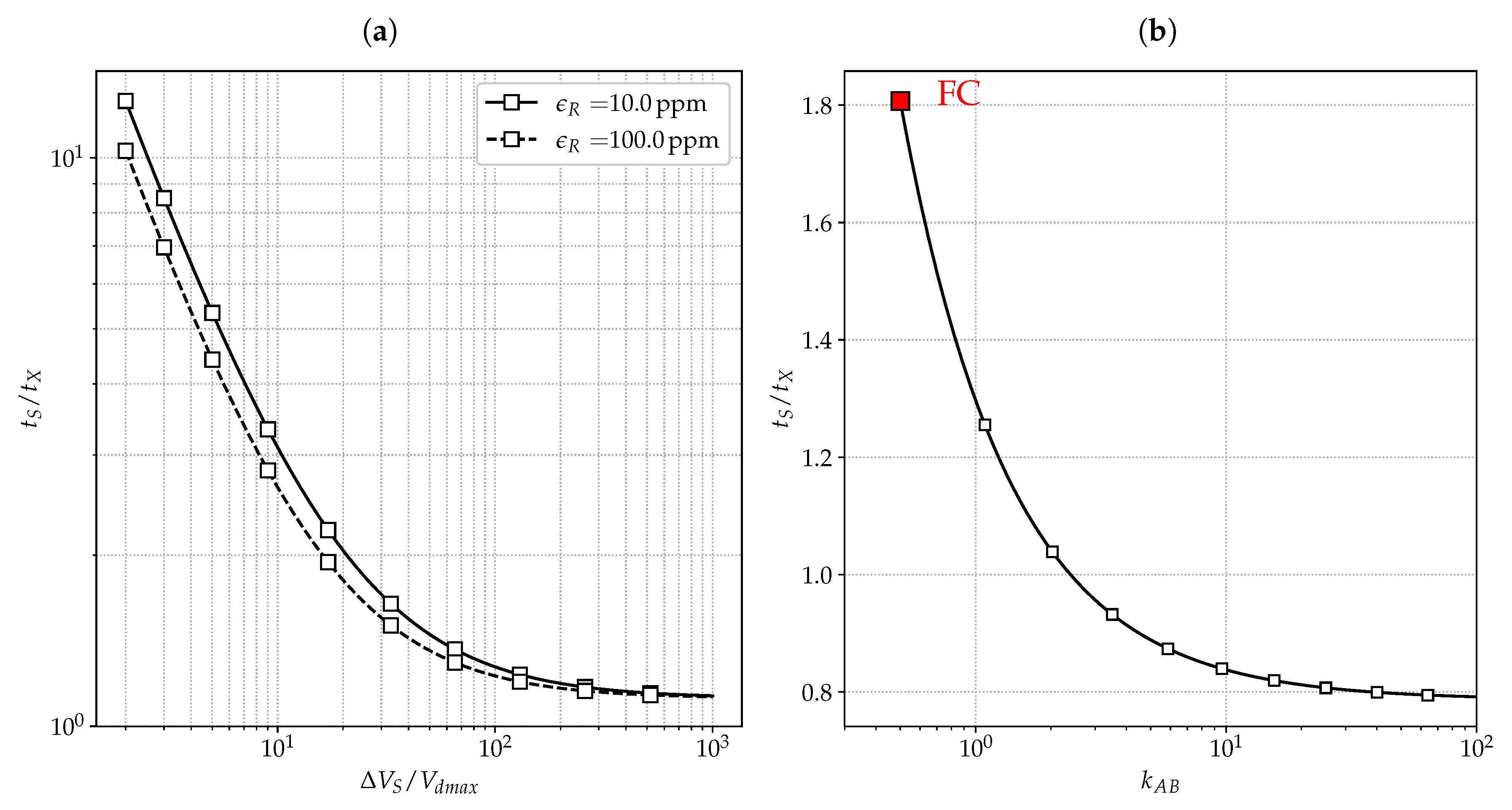
Figure 5a shows the settling time normalized to time calculated by Equation (17) for the OTA of Figure 4 as a function of the ratio. We imagine starting with a large input voltage step , e.g., 2 V, and then imagine varying by sizing the input devices. Large values of , which are beneficial for , can be achieved by reducing which is the remaining degree of freedom in the OTA design when the above mentioned choices on the capacitors are made. The two curves in Figure 5a refer to two different target values of the residual relative error , namely 10 and 100 ppm. For small values of , the linear time represents the main contribution of the whole transient, thus different impacts on according to the logarithmic dependence expressed in Equation (17).
Figure 5.
Normalized settling time behaviour of the circuit in Figure 2a, with pF, pF, pF, pF: (a) FC OTA for relative error ppm and ppm; (b) effect of an ideal SRE to increase of FC OTA, for and ppm.
The first design indication that can be derived from Figure 5a is that, in a single-stage OTA with a fixed supply current budget and fixed maximum magnitude of the input stimulus, the minimum values of the settling time are obtained by minimizing . Note that even pushing the input devices into subthreshold region, cannot be smaller than several of tens millivolts, then, with an input stimulus of the order of a few volts, the feasible values of cannot exceed a few tens, so that the asymptotic behaviour is only a mathematical extrapolation that does not correspond to feasible circuital solutions. The fact that the curves converge at high ratios means that the settling time is dominated by the SR time, which becomes independent of the target residual error when gets negligible with respect to .
The advantage of increasing the maximum output current by means of a parallel-type SRE circuit is illustrated in Figure 5b, where all parameters are kept constant and is swept, starting from the value 1/2, which represents the original OTA of Figure 4 with no SRE applied. For this investigation, parameter was fixed to 20. The curve in Figure 5b clearly indicates that, in a typical SC design case as the one considered here, most of the reduction is obtained with moderate ratios and there is not a real advantage in seeking extreme ratios between the maximum output current and the static supply current. In addition, it is apparent that the maximum advantage is about a factor of 2 for the FC OTA/SRE combination. This result confirms that the application of these output current boosting strategies may only reduce the SR time () to a negligible value, leaving unchanged. Larger relative advantages can be brought by increasing when the target accuracy is lower, since contribution to will be smaller with respect to the contribution of .
In next section, we will investigate the actual advantages that can be obtained by means of Nagaraj’s SRE, showing the main deviation from the simplified model underlying Equation (17) by means of detailed electrical simulations.
3. Slew-Rate Enhancer Design
3.1. Ideal Behaviour and Static Power Overhead of Parallel-Type SRE
We refer to the configuration depicted in Figure 1, where the output currents of both the main OTA and the SRE sum together to the output nodes. In the ideal case, the SRE provides a non-zero output current only during the SR time of the main OTA, concurring to accelerate the circuit settling. The piece-wise linear representation used to model the OTA/SRE output current as a function of the input differential voltage is shown in Figure 3b, where is the sum of the maximum current of the OTA and SRE circuit, indicated with and , respectively. Thus, according to Equation (10):
where and designate the current efficiencies of the main OTA and the SRE, referred to the total current consumption. The introduction of the SRE inevitably introduces a power overhead with respect to the OTA alone, so the total supply current is now calculated as:
Parameter describes the power overhead of the SRE circuit. To obtain an advantage in terms of power vs. settling time trade-off, should be significantly larger than with a negligible power overhead (). One possible implementation of the SRE circuit was proposed by Nagaraj in [42,43]. In the following sections, the Nagaraj’s SRE will be described together with its major limitations. A simple modification of the original scheme, proposed here, shows how these shortcomings are avoided.
3.2. Nagaraj’s SRE
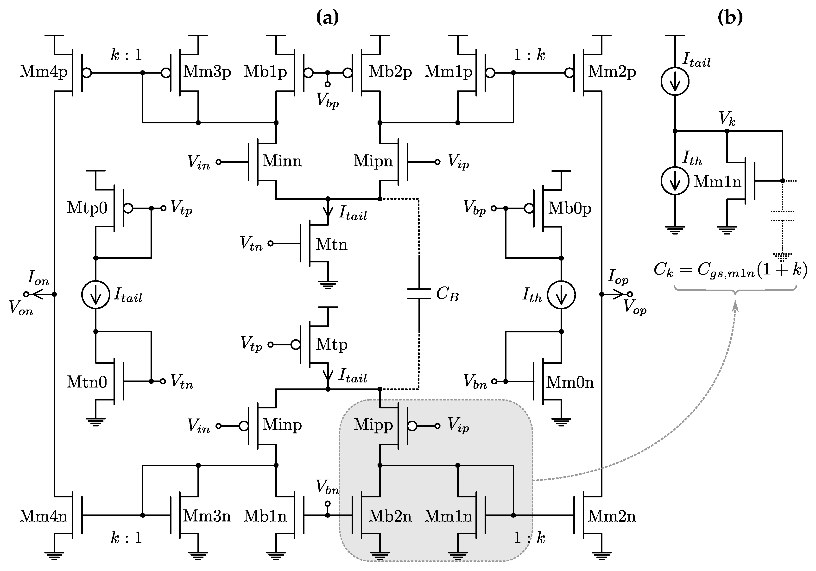
The Nagaraj’s SRE, shown in Figure 6a, can be seen as a derivation of a complementary input pairs mirror-based OTA with shunt current sources implemented through Mb1p-Mb2p and Mb1n-Mb2n. The effect of the shunt current sources is to create a dead zone in the SRE characteristic around the condition. Within the dead zone, all the available current provided by the differential pair is absorbed by the shunt current sources, hence cutting off the current mirrors Mm1p-Mm2p, Mm3p-Mm4p, Mm1n-Mm2n, Mm3n-Mm4n and the output current. In particular, the dead zone is designed to be as large as to guarantee that the mentioned mirrors are all turned off at the end of settling transient. In this way, the SRE output resistance is virtually infinite and no degradation of the OTA dc gain occurs. Due to the dead-zone, no current flows into the four current mirrors for input voltages between and , where the threshold voltage can be tailored by tuning currents and . In order for a dead-zone to exist, the condition should be respected. Furthermore, to allow a non-zero current to be conveyed into the selected mirrors when the input pair is fully unbalanced by a large input voltage, should be greater than . Setting constitutes a robust choice that allows satisfying both conditions with a good margin against process errors. Once currents and are chosen, can be tuned to the desired value by varying the aspect ratio and, consequently, the overdrive voltage of the input devices (Minn-Mipn and Minp-Mipp). In order to approximate as much as possible the characteristic of Figure 3b, was adjusted to be equal to of the main OTA.
Figure 6.
Fully differential Nagaraj’s SRE schematic (a); simplified schematic during turn-on transient (b). The capacitor , not present in the original works of [42,43], is proposed here to reduce the SRE turn-on delay as explained in Section 3.3 and Section 3.4.
The steady-state current consumption of the SRE is , which from Equation (20) is also related to through . This allows us to find a design expression of as
and
Assuming and , .
3.3. SRE Simulations and Turn-On/Off Effects
Apparently, Equation (22) suggests that an arbitrary small can be set for a desired by incrementing k. Electrical simulations have been performed on the circuit depicted in Figure 1, to check whether the reduction expected from Figure 5b can be actually obtained with this approach. The OTA and the SRE are the FC OTA and the Nagaraj’s SRE depicted in Figure 4 and Figure 6, respectively; the circuit was designed with the UMC 180 nm CMOS process under 1.8-V supply condition and was simulated with the SpectreTM simulator. The capacitive network was sized as in the case study used in Figure 5; the relative error was set to 100 ppm. The OTA has been designed with a supply current A, while the SRE supply current is , where will be specified later. The differential input signal V is high enough (in absolute value) to bring the OTA far from its linearity range; the final differential output voltage is V, neglecting the finite dc gain effects. The clock edge controlling the switches’ commutation occurs at 1 s.
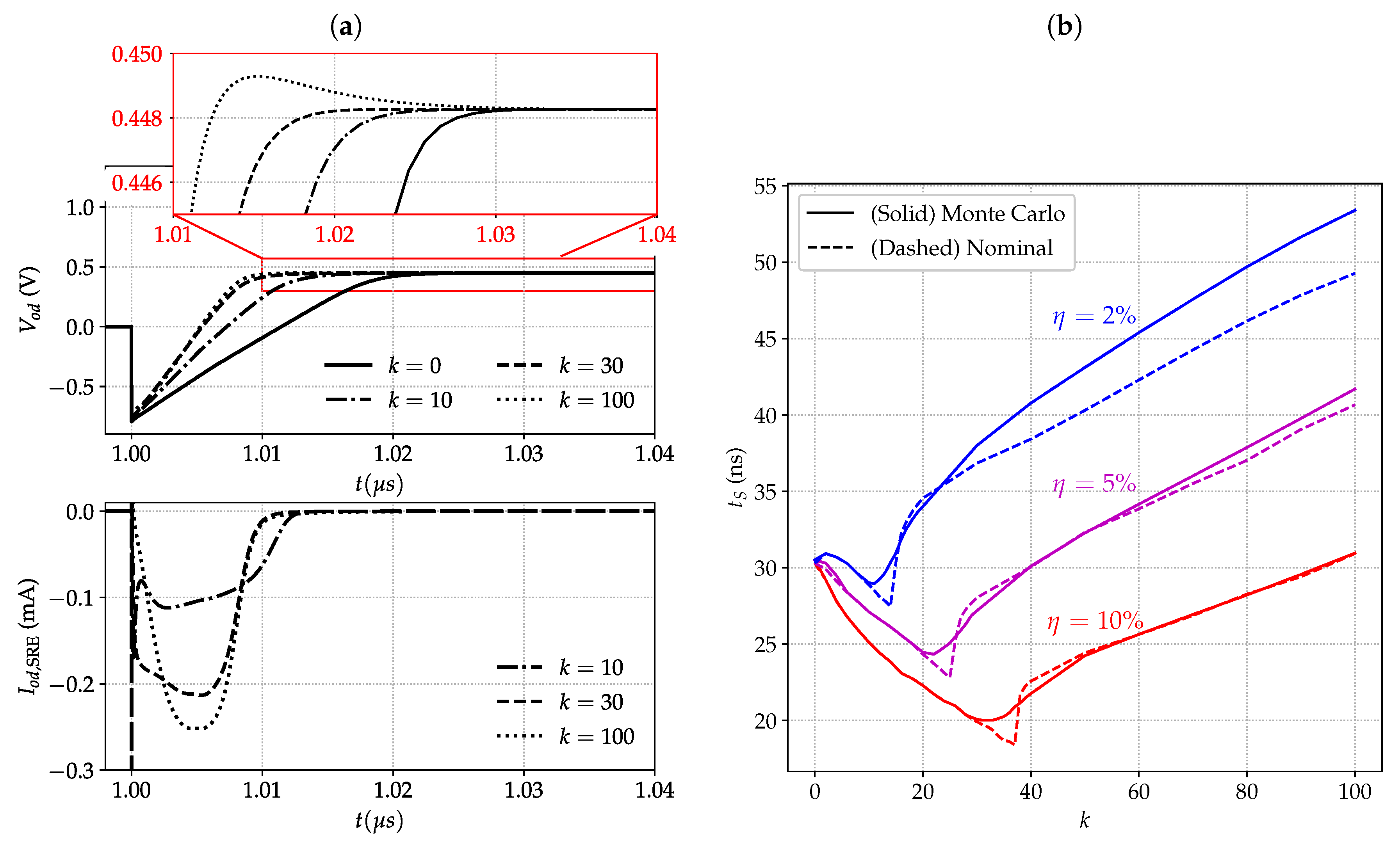
The differential output voltage and the SRE differential output current in Figure 7a are obtained with and different values of the SRE mirroring factor k ( represents the configuration without SRE). Figure 7b shows the settling time vs. k (for different factors), plotting both the nominal case and the average estimated over 100 Monte Carlo (MC) runs. The reason for the latter will be explained later in this section.
Figure 7.
Transient simulations of FC OTA and Nagaraj’s SRE in the configuration shown in Figure 1: (a) Differential output voltage (magnified in the inset) and SRE differential output current for different values of k, for ( represents the case where SRE is not present); (b) Settling time of the OTA and SRE obtained by nominal and Monte Carlo (average on 100 runs) simulations, for different values of and mirroring factors k.
As it looks evident from the curve for in Figure 7b, the settling time is progressively reduced by increasing k, e.g., with and . As an example, the case implies a settling time reduction of respect to of the FC OTA alone. Larger values, obtained by increasing the k factor, would bring the settling time reduction up to , according to the analytical model. However, electrical simulations clearly show that increasing k from 30 to 100 does not introduce further benefits; on the contrary, becomes even higher than the one obtained without SRE. This is qualitatively evident from Figure 7a: the higher SRE output current due to the higher k is not provided as promptly as in the case for . Moreover, an increase of the k factor is followed by a less than proportional increment of . Finally, the delay of the SRE turn-off causes the overshoot of shown in the inset, resulting in a larger time to settle.
To better understand the origin of this turn-on delay, a simplified turn-on transient is described here. For the sake of simplicity, let us consider the turn-on transient of current mirror Mm1n-Mm2p, whose input device is represented in Figure 6b together with the input currents applied when the input voltage step magnitude is large enough to completely unbalance the input differential pair, M1np-M1pp, of the SRE. The current linearly charges the parasitic capacitance at the mirror input until reaches and Mm1n turns on. Then, the transient will be governed by the non-linear differential equation described in [50] and characterized by a time constant
being the transconductance of Mm1n when its drain current is equal to the asymptotic value . This simple model already suggests that the mirror turn-on delay will be aggravated both by large values of k (increased Mm2n gate area) and small values of , i.e., small values of , as confirmed by the simulations shown in Figure 7b: for , indeed, SRE is ineffective or even detrimental for all the k values. Analogous effects occur also during the SRE turn-off transient, but the actual analysis is made more complex by the input stimulus at Mm1n, which cannot be assumed to be an instantaneous current step as in the turn-on transient. However, it is reasonable to assume a turn-off transient with a time constant similar to the one expressed in Equation (23).
An optimum k which minimizes (depending on the value of ) is visible from Figure 7b. This phenomenon has been explained considering that the mentioned turn-off delay may cause the SRE current impulse to stop when the OTA has already entered the linear region, significantly reducing also the linear time . A further increase in the SRE delay would result in overcoming the condition of , producing the overshoot previously described and visible in Figure 7a for . Recovering from this overshoot clearly causes the increase visible at high k values. The hypothesis that this optimum is the result of critical compensation among different contributions suggested to perform Monte-Carlo (MC) simulations to test the robustness of this effect against process variations. The MC curves in Figure 7b are obtained by averaging the settling time extracted from sets of 100 Monte-Carlo runs, involving both local and global process variations. As expected, the minimum is still visible in the MC average, but it is significantly less prominent than in the nominal case.
Another noticeable difference between nominal and MC simulations is present in the case for and . The cause of higher in the MC curves lies in an incomplete turn-off of the Nagaraj’s SRE output branches in some of the MC runs: besides a reduction of the overall output impedance, the incorrect steady state of the OTA/SRE worsens the overall settling time. The incomplete SRE turn-off is due to mismatch in the current mirrors providing and , failing to respect the condition . Note that the factor was varied by keeping the SRE transistor sizing optimized for the case and varying only the bias currents ( and ) proportionally. At small values, the resultant reduction of critical overdrive voltages caused an increase of the matching errors as large as to make smaller than in a few runs, preventing the SRE from completely turning off at the end of the transient. This problem could be arguably solved by resizing the SRE for the smaller bias current of the case.
In summary, the simulated results clearly show that the actual advantage that can be obtained by increasing the ratio, i.e., the ratio, is significantly smaller that the analytical model prediction. This discrepancy is much more evident when we assign a reduced current budget to the SRE. Nevertheless, the analytical model is still useful to estimate the theoretical limit that could be reached if the mentioned internal delays could be overcome. A possible solution that goes in this direction is shown in next section.
3.4. Capacitive-Boosted Nagaraj’s SRE
The fact that the asymptotic settling time reduction predicted by Figure 5b cannot be obtained in practice, due to the mentioned SRE delays, limits the applicability of the described solution for low power applications, where negligible power overheads (i.e., small ) are required. A higher current, in fact, would effectively reduce the internal delays, at the cost of a larger static power consumption. To overcome this limitation, we propose a dynamic current boosting technique which is obtained by simply adding the capacitor between the source terminals of the complementary input differential pairs of the original Nagaraj’s SRE, as depicted in Figure 6a.
Let us consider a large negative voltage step as differential input voltage. The capacitor instantaneously realizes a short circuit, creating a direct path between the power rails through Mm3p, Minn, Mipp, Mm1n. The two turned-on input devices establish a large current flow, which is no more limited by but depends on the input differential voltage in a square law fashion (due to the strong inversion region biasing). This large current impulse will immediately start charging the parasitic capacitances of the current mirrors, e.g., in Figure 6b and will increase the transconductances of the current mirrors, thus reducing the turn-on delay and making the output currents both faster and larger, obtaining an effective SR time reduction.
When operating in a periodic steady state as in typical SC applications, cannot provide an average charge different from zero, because it needs to be periodically recharged by the internal current sources (Mtn and Mtp), but it is able to concentrate its effect in a short time at the beginning of the transient. An analytical model of this phenomenon is very complex and far from the aim of this paper; however, from electrical simulations, it is possible to find an optimum value of the capacitor for each given value of that, together with a proper value of k, minimizes the SR time and consequently .
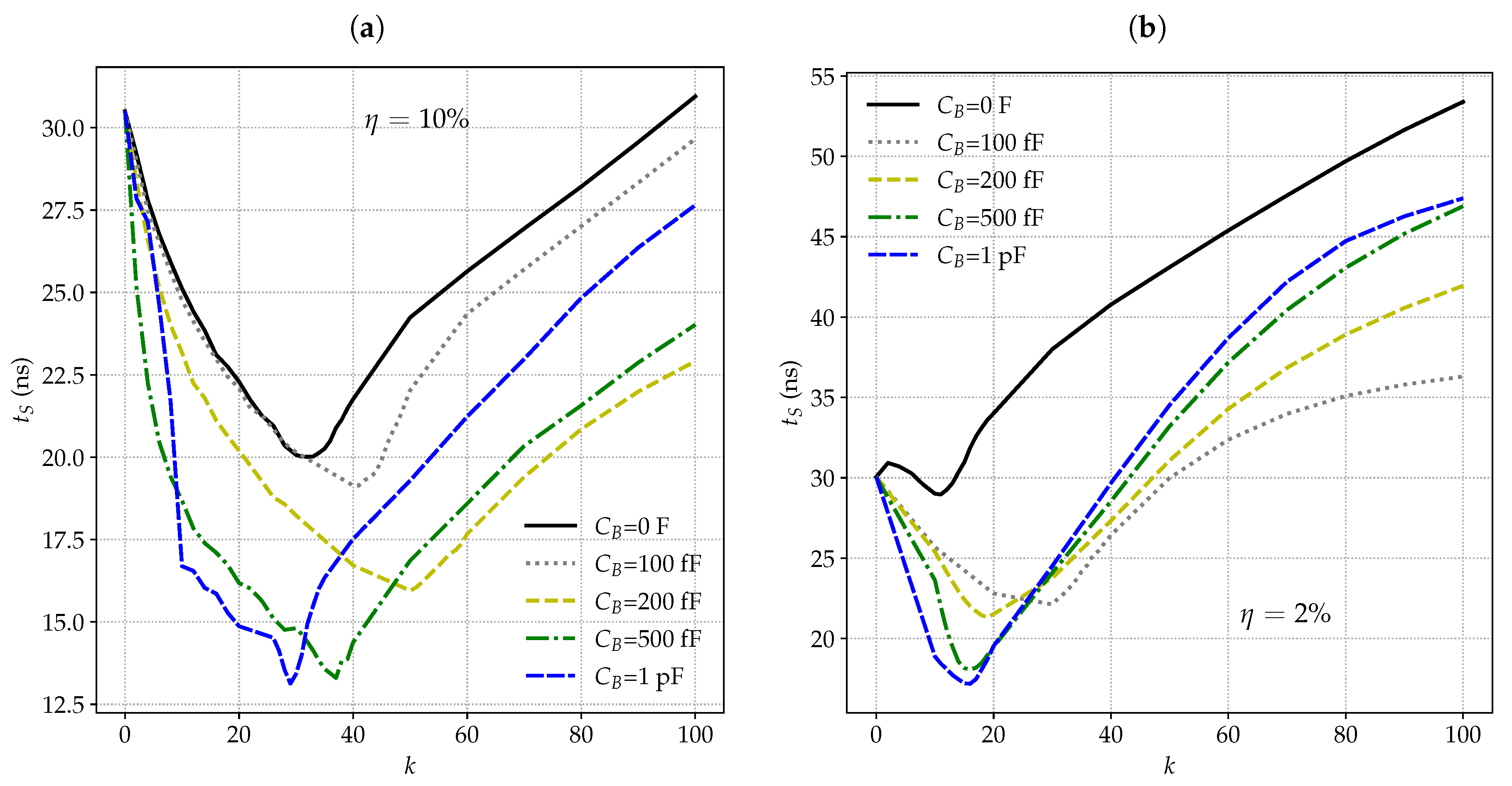
Figure 8 shows the settling time behaviour with respect to the k mirror factor for different values, in two different conditions of static current consumption ( and ). Each point is evaluated averaging over 100 MC runs. In Figure 8a, it looks clear how the increasing of enhances the SRE performance, achieving a reduction of compared to the settling time of the OTA without SRE, consistent with the maximum reduction indicated by the analytical model. For larger than 500 fF, no further benefits are obtained. Figure 8b shows the effectiveness of even in the case of , when the Nagaraj’s SRE was not able to introduce benefits: for fF, settling time reductions up to can be achieved.
Figure 8.
Settling time (averaged on 100 MC runs) with Capacitive-Boosted Nagaraj’s SRE for different boosting capacitances and mirroring ratios k: (a) for ; (b) for .
Note that the monotonic behaviour of as function of in Figure 5b is not respected also for the boosted SRE, since increases at high k values, corresponding to high values. Indeed, very large output current gains are obtained by increasing the width (and then gate area) of the output devices to such an extent that even the boosted current impulse is unable to overcome the internal delay. In addition, it should be observed that the turn-off delay is likely to be less affected by the presence of capacitor , since the SRE switch-off is not commanded by a large voltage step as the turning-on event, but by an input voltage that is evolving in the linear operating zone of the SRE input pairs. However, as the results of Figure 8 clearly prove, the reduction that can be obtained at moderate values of k gains with the modified SRE reaches the asymptotic values predicted by the simple model described in Section 2.
4. Conclusions
Simulation results performed on the combination of the FC OTA cascode with the original Nagaraj’s SRE showed that the latter is unable to produce the settling time reduction predicted by a simple model that neglects internal delays of both the OTA and SRE units. The effectiveness of the Nagaraj’s SRE progressively degrades as its relative power overhead (the factor) is diminished. This might be the reason of the limited presence in the literature of this kind of slew rate enhancing approach, albeit its attracting characteristics and, in particular, the fact that it completely turns off at the end of the transient, leaving the noise, offset and gain properties of the original OTA unchanged. Analysis of the output current dynamics reveals that high gains of the output mirrors, required to achieve adequate power efficiencies, resulted in a significant delay in the delivery of the output current impulse, making the SRE ineffective or even detrimental.
This problem was solved by the simple introduction of a bypass capacitor (), which turned the original Nagaraj’s SRE in what is here dubbed capacitive-boosted SRE. The simulation results clearly show that this simple modification allowed the capacitive-boosted SRE to provide benefits, in terms of settling time reduction, that reach the prediction of the simplified analytical model in the case of a 10% power overhead, and, more remarkably, get close to the predicted 50% reduction even for a small 2% power overhead, at which the original Nagaraj’s SRE was completely ineffective. Finally, we emphasize the fact that these improvements are obtained at the cost, in terms of silicon area, of only the accommodation of a sub-pF capacitor.
Author Contributions
All authors participated to the conceptualization and methodology of this work. Data curation, A.C., M.C.; writing—original draft preparation, A.C., M.C., M.D.; writing—review and editing: M.P., P.B. All authors have read and agreed to the published version of the manuscript.
Funding
This project has received funding from the European Union’s Horizon 2020 research and innovation programme under the Marie Skłodowska-Curie grant agreement No. 893544.
Conflicts of Interest
The authors declare no conflict of interest. The funders had no role in the design of the study; in the collection, analyses, or interpretation of data; in the writing of the manuscript, or in the decision to publish the results.
References
- Carvajal, R.G.; Ramirez-Angulo, J.; Lopez-Martin, A.J.; Torralba, A.; Galan, J.A.G.; Carlosena, A.; Chavero, F.M. The flipped voltage follower: A useful cell for low-voltage low-power circuit design. IEEE Trans. Circuits Syst. I Regul. Pap. 2005, 52, 1276–1291. [Google Scholar] [CrossRef]
- Hosticka, B.J. Dynamic CMOS amplifiers. IEEE J. Solid-State Circuits 1980, 15, 881–886. [Google Scholar] [CrossRef]
- Peluso, V.; Vancorenland, P.; Steyaert, M.; Sansen, W. 900 mV differential class AB OTA for switched opamp applications. Electron. Lett. 1997, 33, 1455–1456. [Google Scholar] [CrossRef]
- Harjani, R.; Heineke, R.; Wang, F. An integrated low-voltage class AB CMOS OTA. IEEE J. Solid-State Circuits 1999, 34, 134–142. [Google Scholar] [CrossRef]
- Bernal, M.R.V.; Celma, S.; Medrano, N.; Calvo, B. An Ultralow-Power Low-Voltage Class-AB Fully Differential OpAmp for Long-Life Autonomous Portable Equipment. IEEE Trans. Circuits Syst. II Express Briefs 2012, 59, 643–647. [Google Scholar] [CrossRef]
- Vi, S.; Gupta, A.; Mittal, A. An Operational Amplifier with Recycling Folded Cascode Topology and Adaptive Biasing. Int. J. VLSI Des. Commun. Syst. 2014, 5. [Google Scholar] [CrossRef]
- Akbari, M.; Hashemipour, O.; Moradi, F. A High Slew Rate CMOS OTA with Dynamic Current Boosting Paths. In Proceedings of the 2018 IEEE International Symposium on Circuits and Systems (ISCAS), Florence, Italy, 27–30 May 2018; pp. 1–5. [Google Scholar]
- Degrauwe, M.G.; Rijmenants, J.; Vittoz, E.A.; Man, H.J.D. Adaptive biasing CMOS amplifiers. IEEE J. Solid-State Circuits 1982, 17, 522–528. [Google Scholar] [CrossRef]
- Huang, B.; Xu, L.; Chen, D. Slew rate enhancement via excessive transient feedback. Electron. Lett. 2013, 49, 930–932. [Google Scholar] [CrossRef]
- Hung, C.H.; Zheng, Y.; Guo, J.; Leung, K.N. Bandwidth and Slew Rate Enhanced OTA with Sustainable Dynamic Bias. IEEE Trans. Circuits Syst. II: Express Briefs 2020, 67, 635–639. [Google Scholar] [CrossRef]
- Nizza, N.; Mondini, A.; Bruschi, P. A current feedback adaptive biasing method for class-AB OTA cells. In Proceedings of the PRIME 2005, Lausanne, Switzerland, 28 July 2005; pp. 390–393. [Google Scholar]
- Cai, C.; Chen, D. A slew-rate enhancement technique for fully differential amplifier without inducing Trojan state. In Proceedings of the 2015 IEEE 58th International Midwest Symposium on Circuits and Systems (MWSCAS), Fort Collins, CO, USA, 2–5 August 2015; pp. 1–4. [Google Scholar]
- Ramirez-Angulo, J. A novel slew-rate enhancement technique for one-stage operational amplifiers. In Proceedings of the 39th Midwest Symposium on Circuits and Systems, Ames, IA, USA, 21–21 August 1996; Volume 1, pp. 7–10. [Google Scholar]
- Lopez-Martin, A.J.; Baswa, S.; Ramirez-Angulo, J.; Carvajal, R.G. Low-Voltage Super class AB CMOS OTA cells with very high slew rate and power efficiency. IEEE J. Solid-State Circuits 2005, 40, 1068–1077. [Google Scholar] [CrossRef]
- Galan, J.A.; Lopez-Martin, A.J.; Carvajal, R.G.; Ramirez-Angulo, J.; Rubia-Marcos, C. Super Class-AB OTAs With Adaptive Biasing and Dynamic Output Current Scaling. IEEE Trans. Circuits Syst. Regul. Pap. 2007, 54, 449–457. [Google Scholar] [CrossRef]
- Wan, X.P.; Zhang, F.X.; Zhen, S.W.; He, Y.J.; Luo, P. Efficient slew-rate enhanced operational transconductance amplifier. J. Electron. Sci. Technol. 2015, 13, 14–19. [Google Scholar]
- Sutula, S.; Dei, M.; Terés, L.; Serra-Graells, F. Variable-Mirror Amplifier: A New Family of Process-Independent Class-AB Single-Stage OTAs for Low-Power SC Circuits. IEEE Trans. Circuits Syst. Regul. Pap. 2016, 63, 1101–1110. [Google Scholar] [CrossRef]
- Yan, Z.; Mak, P.; Law, M.; Martins, R.P.; Maloberti, F. Nested-Current-Mirror Rail-to-Rail-Output Single-Stage Amplifier With Enhancements of DC Gain, GBW and Slew Rate. IEEE J. Solid-State Circuits 2015, 50, 2353–2366. [Google Scholar] [CrossRef]
- Lee, J.; Song, S.; Roh, J. A 103 dB DR Fourth-Order Delta-Sigma Modulator for Sensor Applications. Electronics 2019, 8, 1093. [Google Scholar] [CrossRef]
- Roh, J. High-Gain Class-AB OTA with Low Quiescent Current. Analog. Integr. Circuits Signal Process. 2006, 47, 225–228. [Google Scholar] [CrossRef]
- Assaad, R.S.; Silva-Martinez, J. The Recycling Folded Cascode: A General Enhancement of the Folded Cascode Amplifier. IEEE J. Solid-State Circuits 2009, 44, 2535–2542. [Google Scholar] [CrossRef]
- Li, Y.L.; Han, K.F.; Tan, X.; Yan, N.; Min, H. Transconductance enhancement method for operational transconductance amplifiers. Electron. Lett. 2010, 46, 1321–1323. [Google Scholar]
- Yavari, M. Single-Stage Class AB Operational Amplifier for SC Circuits. Electron. Lett. 2010, 46, 977–979. [Google Scholar] [CrossRef]
- Zhao, X.; Fang, H.; Xu, J. A new low power symmetric folded cascode amplifier by recycling current in 65 nm CMOS technology. In Proceedings of the 9th IEEE International Conference on ASIC, Xiamen, China, 25–28 October 2011; pp. 820–823. [Google Scholar]
- Akbari, M. Single-stage fully recycling folded cascode OTA for switched-capacitor circuits. Electron. Lett. 2015, 51, 977–979. [Google Scholar] [CrossRef]
- Garde, M.P.; Lopez-Martin, A.J.; Carvajal, R.G.; Galan, J.A.; Ramirez-Angulo, J. Super class AB RFC OTA using non-linear current mirrors. Electron. Lett. 2018, 54, 1317–1318. [Google Scholar] [CrossRef]
- Garde, M.P.; Lopez-Martin, A.J.; Carvajal, R.G.; Ramirez-Angulo, J. Super class AB RFC OTA with adaptive local common-mode feedback. Electron. Lett. 2018, 54, 1272–1274. [Google Scholar] [CrossRef]
- Garde, M.P.; Lopez-Martin, A.; Carvajal, R.G.; Ramrez-Angulo, J. Super Class-AB Recycling Folded Cascode OTA. IEEE J. Solid-State Circuits 2018, 53, 2614–2623. [Google Scholar] [CrossRef]
- Wang, Y.; Zhang, Q.; Yu, S.S.; Zhao, X.; Trinh, H.; Shi, P. A Robust Local Positive Feedback Based Performance Enhancement Strategy for Non-Recycling Folded Cascode OTA. IEEE Trans. Circuits Syst. Regul. Pap. 2020, 67, 2897–2908. [Google Scholar] [CrossRef]
- Cisneros-Fernández, J.; Terés, L.; Dei, M.; Serra-Graells, F. Design methodology for power-efficient SC delta-sigma modulators based on switched-VMAs. In Proceedings of the 2017 32nd Conference on Design of Circuits and Integrated Systems (DCIS), Barcelona, Spain, 22–24 November 2017; pp. 1–6. [Google Scholar]
- Silva-Martinez, J.; Yan, T.; Jiang, J.; Shao, J. Efficient Broadband Class AB Amplifier. In Proceedings of the 2019 IEEE 62nd International Midwest Symposium on Circuits and Systems (MWSCAS), Dallas, TX, USA, 4–7 August 2019; pp. 1045–1048. [Google Scholar]
- Algueta-Miguel, J.M.; Lopez-Martin, A.; Garde, M.P.; De, C.A. La Cruz and J. Ramirez-Angulo, ±0.5 V 15 μW Recycling Folded Cascode Amplifier With 34,767 MHz·pF/mA FOM. IEEE Solid State Circuits Lett. 2018, 1, 170–173. [Google Scholar] [CrossRef]
- Garde, M.P.; Lopez-Martin, A.; Algueta, J.M.; Carvajal, R.G.; Ramirez-Angulo, J. Class AB amplifier with enhanced slew rate and GBW. Int. J. Circ. Theor. Appl. 2019, 47, 1199–1210. [Google Scholar] [CrossRef]
- Perez, A.P.; Kumar, Y.B.N.; Bonizzoni, E.; Maloberti, F. Slew-rate and gain enhancement in two stage operational amplifiers. In Proceedings of the 2009 IEEE International Symposium on Circuits and Systems (ISCAS), Taipei, Taiwan, 24–27 May 2009; pp. 2485–2488. [Google Scholar]
- Naderi, M.H.; Prakash, S.; Silva-Martinez, J. Operational Transconductance Amplifier With Class-B Slew-Rate Boosting for Fast High-Performance Switched-Capacitor Circuits. IEEE Trans. Circuits Syst. Regul. Pap. 2018, 65, 3769–3779. [Google Scholar] [CrossRef]
- Lee, H.; Mok, P.K.T. A CMOS current-mirror amplifier with compact slew rate enhancement circuit for large capacitive load applications. In Proceedings of the The 2001 IEEE International Symposium on Circuits and Systems, Sydney, NSW, Australia, 6–9 May 2001; Volume 1, pp. 220–223. [Google Scholar]
- Lee, H.; Mok, P.K.T. Single-point-detection slew-rate enhancement circuits for single-stage amplifiers. In Proceedings of the 2002 IEEE International Symposium on Circuits and Systems, Proceedings (Cat. No.02CH37353), Phoenix-Scottsdale, AZ, USA, 26–29 May 2002. [Google Scholar]
- Rezaei, M.; Zhian-Tabasy, E.; Ashtiani, S.J. Slew rate enhancement method for folded-cascode amplifiers. Electron. Lett. 2008, 44, 1226–1228. [Google Scholar] [CrossRef]
- Leung, K.; Ng, Y. A CMOS voltage buffer with slew-rate enhancement. Int. J. Electron. 2013, 101, 820–830. [Google Scholar] [CrossRef]
- Bu, S.; Tse, H.W.; Leung, K.N.; Guo, J.; Ho, M. Gain and slew rate enhancement for amplifiers through current starving and feeding. In Proceedings of the 2015 IEEE International Symposium on Circuits and Systems (ISCAS), Lisbon, Portugal, 24–27 May 2015; pp. 2073–2076. [Google Scholar]
- Akbari, M.; Hassanzadeh, A.; Hashemipour, O. Slew rate boosting technique for an upgraded transconductance amplifier. Analog. Integr. Circuits Signal Process. 2016, 88, 57–63. [Google Scholar] [CrossRef]
- Nagaraj, K. Slew rate enhancement method for folded-cascode amplifiers. Electron. Lett. 1989, 25, 1226–1228. [Google Scholar]
- Nagaraj, K. CMOS amplifiers incorporating a novel slew rate enhancement technique. In Proceedings of the IEEE Proceedings of the Custom Integrated Circuits Conference, Boston, MA, USA, 13–16 May 1990; pp. 11.6/1–11.6/5. [Google Scholar]
- Tan, C.; Chen, Z. An efficient CMOS operational amplifier for driving large capacitive loads. In Proceedings of the 2007 7th International Conference on ASIC, Guilin, China, 22–25 October 2007; pp. 643–646. [Google Scholar]
- Kareppagoudr, M.; Caceres, E.; Kuo, Y.; Shakya, J.; Wang, Y.; Temes, G.C. Passive slew rate enhancement technique for Switched-Capacitor Circuits. In Proceedings of the 2019 IEEE 62nd International Midwest Symposium on Circuits and Systems (MWSCAS), Dallas, TX, USA, 4–7 August 2019; pp. 913–916. [Google Scholar]
- Haug, K.; Maloberti, F.; Temes, G.C. Switched-capacitor integrators with low finite-gain sensitivity. Electron. Lett. 1985, 21, 1156–1157. [Google Scholar] [CrossRef]
- Martin, K.; Ozcolak, L.; Lee, Y.S.; Temes, G.C. A differential switched-capacitor amplifier. IEEE J. Solid-State Circuits 1987, 22, 104–106. [Google Scholar] [CrossRef]
- Martin, K.; Sedra, A.S. Strays-insensitive switched-capacitor filters based on bilinear Z-transform. Electron. Lett. 1979, 15, 365–366. [Google Scholar] [CrossRef]
- del Rio, R.; Medeiro, F.; Perez-Verdu, B.; Rodriguez-Vazquez, A. Reliable analysis of settling errors in SC integrators-application to the design of high-speed ΣΔ modulators. In Proceedings of the 2000 IEEE International Symposium on Circuits and Systems (ISCAS), Geneva, Switzerland, 28–31 May 2000; Volume 4, pp. 417–420. [Google Scholar]
- Nairn, D.G. Analytic Step Response of MOS Current Mirrors. IEEE Trans. Circuits Syst. Fundam. Theory Appl. 1993, 40, 133–135. [Google Scholar] [CrossRef]
Publisher’s Note: MDPI stays neutral with regard to jurisdictional claims in published maps and institutional affiliations. |
© 2020 by the authors. Licensee MDPI, Basel, Switzerland. This article is an open access article distributed under the terms and conditions of the Creative Commons Attribution (CC BY) license (http://creativecommons.org/licenses/by/4.0/).