Article

Numerical Simulation Analysis of Switching Characteristics in the Source-Trench MOSFET’s

Department of Electronic Engineering, Sogang University, Seoul 04107, Korea
*
Author to whom correspondence should be addressed.
Electronics 2020, 9(11), 1895; https://doi.org/10.3390/electronics9111895
Submission received: 12 October 2020 / Revised: 30 October 2020 / Accepted: 5 November 2020 / Published: 11 November 2020
(This article belongs to the Section Power Electronics)

Abstract

:
In this paper, we compare the static and switching characteristics of the 4H-SiC conventional UMOSFET (C-UMOSFET), double trench MOSFET (DT-MOSFET) and source trench MOSFET (ST-MOSFET) through TCAD simulation. In particular, the effect of the trenched source region and the gate trench bottom P+ shielding region on the capacitance is analyzed, and the dynamic characteristics of the three structures are compared. The input capacitance is almost identical in all three structures. On the other hand, the reverse transfer capacitance of DT-MOSFET and ST-MOSFET is reduced by 44% and 24%, respectively, compared to C-UMOSFET. Since the reverse transfer capacitance of DT-MOSFET and ST-MOSFET is superior to that of C-UMOSFET, it improves high frequency figure of merit (HF-FOM: RON-SP × QGD). The HF-FOM of DT-MOSFET and ST-MOSFET is 289 mΩ∙nC, 224 mΩ∙nC, respectively, which is improved by 26% and 42% compared to C-UMOSFET. The switching speed of DT-MOSFET and ST-MOSFET are maintained at the same level as the C-UMOSFET. The switching energy loss and power loss of the DT-MOSFET and ST-MOSFET are slightly improved compared to C-UMOSFET.

1. Introduction

4H-SiC MOSFETs are widely considered to be the leading next-generation power semiconductor devices due to their superior material properties, such as high critical electric field, high thermal conductivity, and ability to operate at high temperatures [1,2]. Of the various SiC MOSFET structures, gate-trench MOSFETs (UMOSFETs) typically have lower on-state resistance compared to planar MOSFETs (VDMOSFETs). In addition, UMOSFETs have higher channel density and mobility than VDMOSFETs due to their ability to form vertical channels on the trench sidewalls and their ability to reduce cell pitch [3,4,5,6,7]. However, there are two main drawbacks to UMOSFETs. First, they have a relatively large reverse transfer capacitance (Crss). For high-frequency applications, devices must have a small Miller plateau (QGD) and Crss [8]. Since QGD and Crss are determined by the overlap between the gate and the drain, the gate-trench structure has a relatively large Crss. As such, it is necessary to reduce the device Crss to ensure high power efficiency and low energy loss in high frequency operations. The second problem with UMOSFETs is the appearance of gate oxide reliability issues that arise from the gate oxide at the bottom of the trench when UMOSFET operates in the off-state. Because SiC, a wide bandgap material, has a small offset between the conduction band and the valance band with respect to the SiC and the gate oxide, Fowler Nordheim tunneling (FN tunneling) will occur in the electric field (generally over 3 MV/cm) smaller than Si (~6 MV/cm). This FN tunneling current leads to oxide degradation [9,10,11]. Therefore, in the case of SiC UMOSFETs, it is very important to suppress electric field crowding at the gate oxide edge. To address this problem, a structure which includes a gate trench bottom P+ shielding region (BPR) has been proposed [12,13,14,15]. Various other structures have been proposed additionally to reduce the electric field of the gate oxide [16,17,18,19]. Infineon’s CoolSiC and Rohm’s Double Trench structure were also commercialized at a 1.2 kV class [20,21,22]. Among them, the double trench structures have been most actively studied in recent years with regard to their dynamic properties and reliability [23,24,25]. In the case of the double trench structure, the source region and gate are both trenched. As a result, the electric field is not concentrated in the gate trench region. As a variant of the double trench, a source trench structure for distributing the electric field through thermally grown oxide has been proposed [26]. However, the dynamic characteristics of the 1700 V source trench MOSFET structure have not been actively discussed. In this study, we researched the switching characteristics of the 1700 V UMOSFET, Double Trench MOSFET (DT-MOSFET), and Source Trench MOSFET (ST-MOSFET) structures.

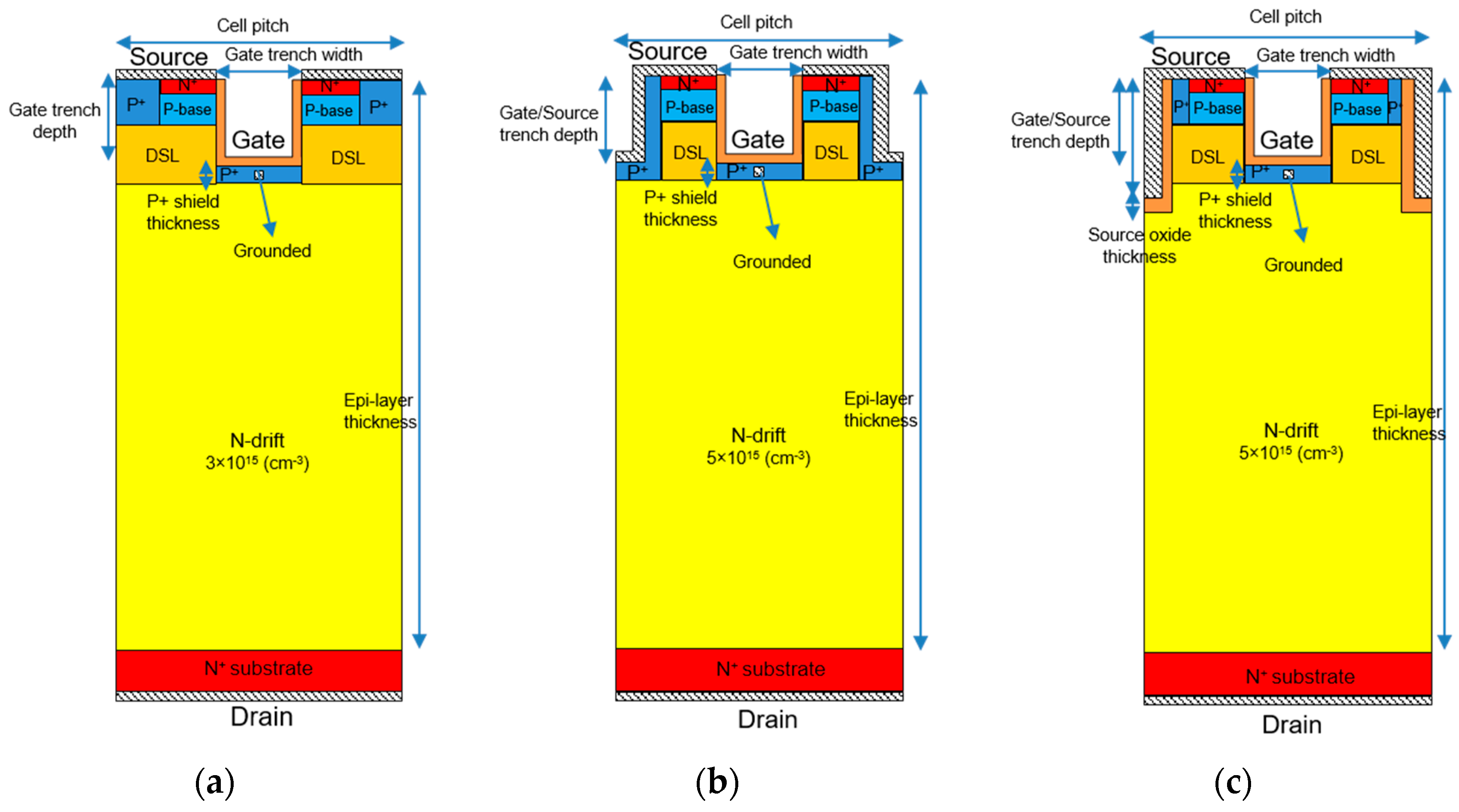
2. Device Structures

Figure 1 shows the three structures considered in this paper. Figure 1a is the conventional UMOSFET (C-UMOSFET), and Figure 1b,c are DT-MOS and ST-MOS, respectively. The device parameters of each structure have been optimized for static characteristics while the BPR is grounded. In addition, a depletion stopping layer (DSL) [27], also known as a current spreading layer (CSL) [28,29], is added. The DSL improves the on-state characteristics by suppressing the expansion of the depletion region in the JFET region. The cell pitch of each structure is 5.55 μm, and the total thickness of the epi-layer is 18 μm. The thickness of the BPR is 0.3 μm, and the gate trench width and depth are 1.55 μm and 1.5 μm, respectively. In the case of DT-MOS, the source trench width is 0.5 um, the depth is 1.5 μm, and the thickness of the P+ shielding region of the source trench is 0.3 μm. In the case of ST-MOS, the source trench width is 0.5 μm, the depth is 2.4 μm, and the source oxide thickness is 0.1 μm. In addition, the concentration of the epi layer of each structure is 3 × 1015 cm−3, 5 × 1015 cm−3, and 5 × 1015 cm−3 for C-UMOS, DT-MOS, and ST-MOS, respectively. Additional device parameters are listed in Table 1.
In the next section, the characteristics of each structure are described. Static characteristics were simulated using Synopsys TCAD, and dynamic characteristics were analyzed through mixed mode simulation [30]. Electron/hole continuity equations and Poisson equation are solved with Shockley–Read–Hall recombination and Auger recombination model. The doping dependency, high field velocity saturation and mobility degradation are included in the mobility model. In particular, the Lombardi model was considered for the interface that affects the channel mobility [31]. Bandgap narrowing, anisotropic material properties, and incomplete ionization effects of each structure were considered [32,33].

3. Results and Discussion

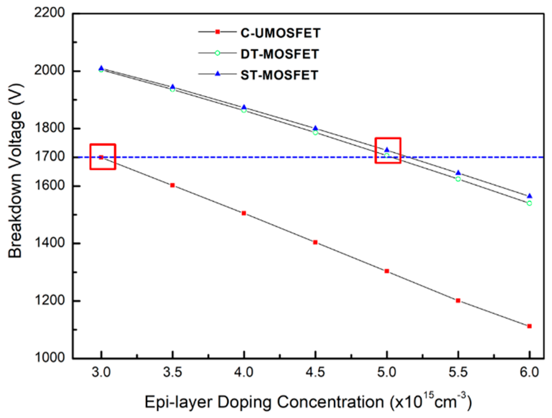
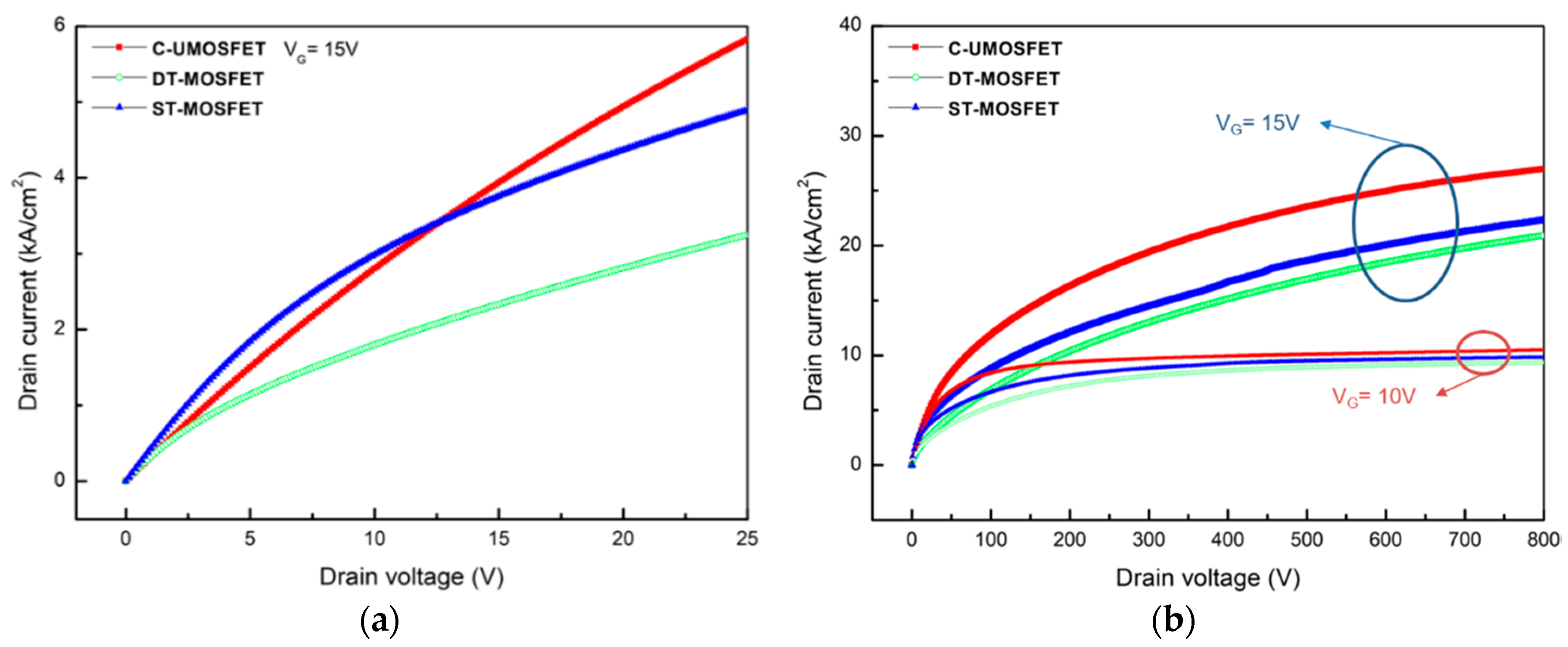
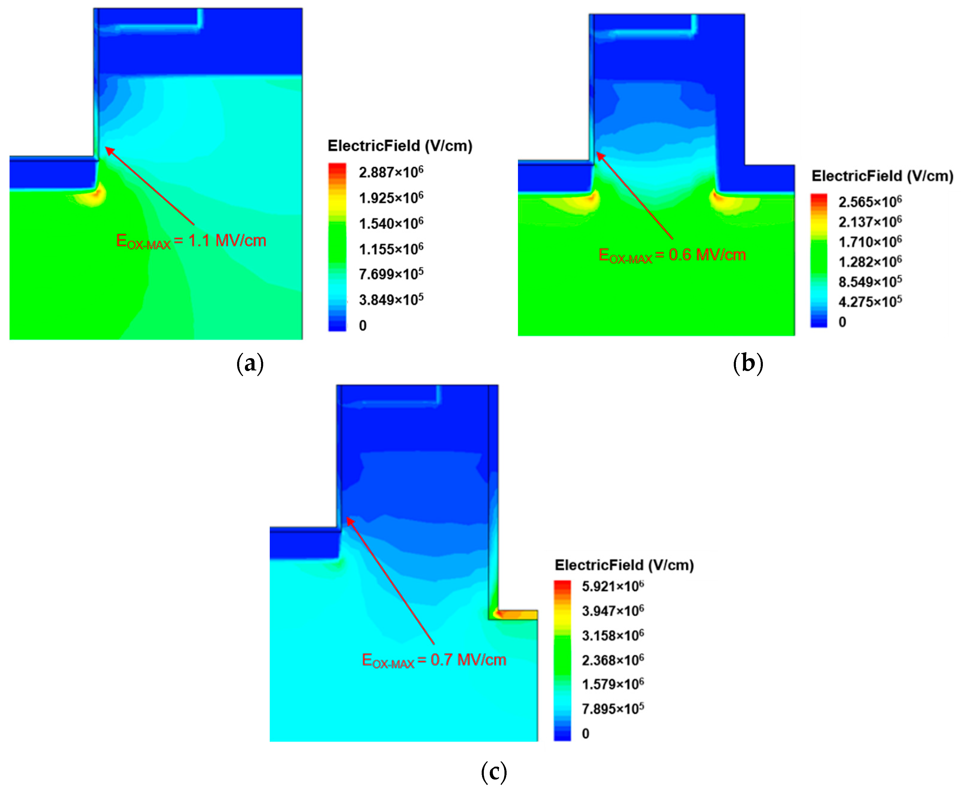
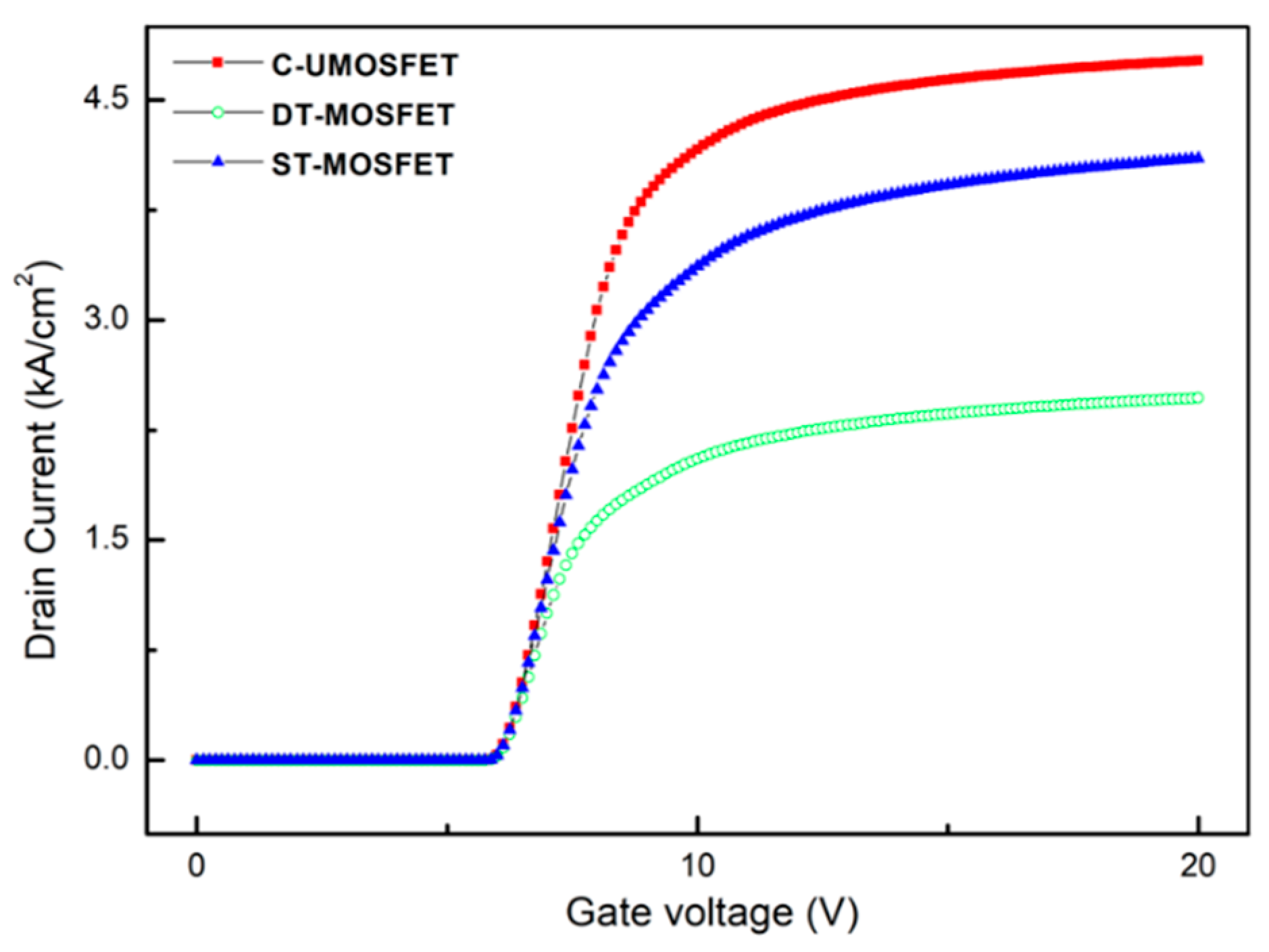
3.1. Static Characteristics

First, in order to facilitate normalization, the active area was assumed to be 1 cm2, and simulation of static characteristics was performed. Figure 2 shows the off-state characteristic curves of the three structures. The breakdown voltages are 1699 V, 1706 V, and 1724 V for each C-UMOSFET, DT-MOSFET and ST-MOSFET, respectively. Figure 3 shows the breakdown voltage when the doping concentration of the epi-layer of each structure is varied. Each structure is designed to have the breakdown voltage close to 1700 V by controlling the doping concentration of the epi-layer. Figure 4 shows the on-state characteristic curves of the three structures when the gate voltage is 15 V. Figure 4a is the on-state characteristic curves of the linear region with the drain voltage range of 0–25 V, and b is the overall on-state characteristic curves with the drain voltage range of 0–800 V. In Figure 4a, the specific on-resistance at a low VD of the C-UMOSFET, DT-MOSFET, and ST-MOSFET are 3.37 mΩ∙cm2, 3.57 mΩ∙cm2, and 2.52 mΩ∙cm2 (at VG = 15 V and ID = 20 A), respectively. From Figure 4b, the quasi-saturation current [34] was highest for C-UMOSFET and lowest for DT-MOSFET. Due to the trenched source region, the width of the JFET region of the DT-MOSFET and ST-MOSFET is smaller than that of the C-UMOSFET. Since the current path decreases in proportion to the JFET width, the quasi-saturation current of DT-MOSFET and ST-MOSFET is reduced compared to the C-UMOSFET. The FOM (BV2/Ron-sp) [35], which represents the trade-off relationship of static characteristics, was calculated as 856.6 MW/cm2, 815.2 MW/cm2, and 1179.4 MW/cm2 for the three structures, C-UMOSFET, DT-MOSFET, and ST-MOSFET, respectively.
Figure 5 shows the off-state gate oxide electric field distributions of each structure when VG = 0 V and VD = 1200 V. The maximum gate oxide electric field (Eox-max) is 1.1 MV/cm for the C-UMOSFET, 0.6 MV/cm for the DT-MOSFET, and 0.7 MV/cm for the ST-MOSFET. The grounded BPR applied to all three structures effectively blocks the electric field at gate oxide, reducing the Eox-max. In the case of the DT-MOSFET and ST-MOSFET, not only the BPR but also the trenched source region disperses the electric field applied to the gate oxide, further reducing the Eox-max. Figure 6 shows the transfer characteristic curves of the three structures at VD = 20 V. As shown, at the same given gate voltage, the current handling capability varies with the JFET width. The wider the JFET width, the larger the drain current at the same gate voltage. Furthermore, the threshold voltages (Vth) calculated at VD = 20 V and ID = 1 A are 5.74 V, 5.75 V, and 5.75 V for each structure. Since the doping concentration and depth of the P-base were kept constant, there was little Vth shift. The overall static performance of the three structure is summarized in Table 2. Figure 7a shows the change in the threshold voltage of each structure as the temperature varies, and the threshold voltage shows the negative temperature coefficient [36]. As the lattice temperature increases from 300 K to 500 K, the threshold voltage decreases due to the increase in intrinsic carrier concentration [37]. In all three structures, the threshold voltage at 500 K decreases by nearly 24% compared to the value at 300 K. Figure 7b shows the specific on-resistance versus temperature. As seen in Figure 7b, the DT-MOSFET is the least temperature dependent, increasing by approximately 140% at 500 K, with respect to its on-resistance at 300 K. For the ST-MOSFET and C-UMOSFET, the on-resistance at 500 K increases by 160% and 180%, respectively, compared to the on-resistance at 300 K.

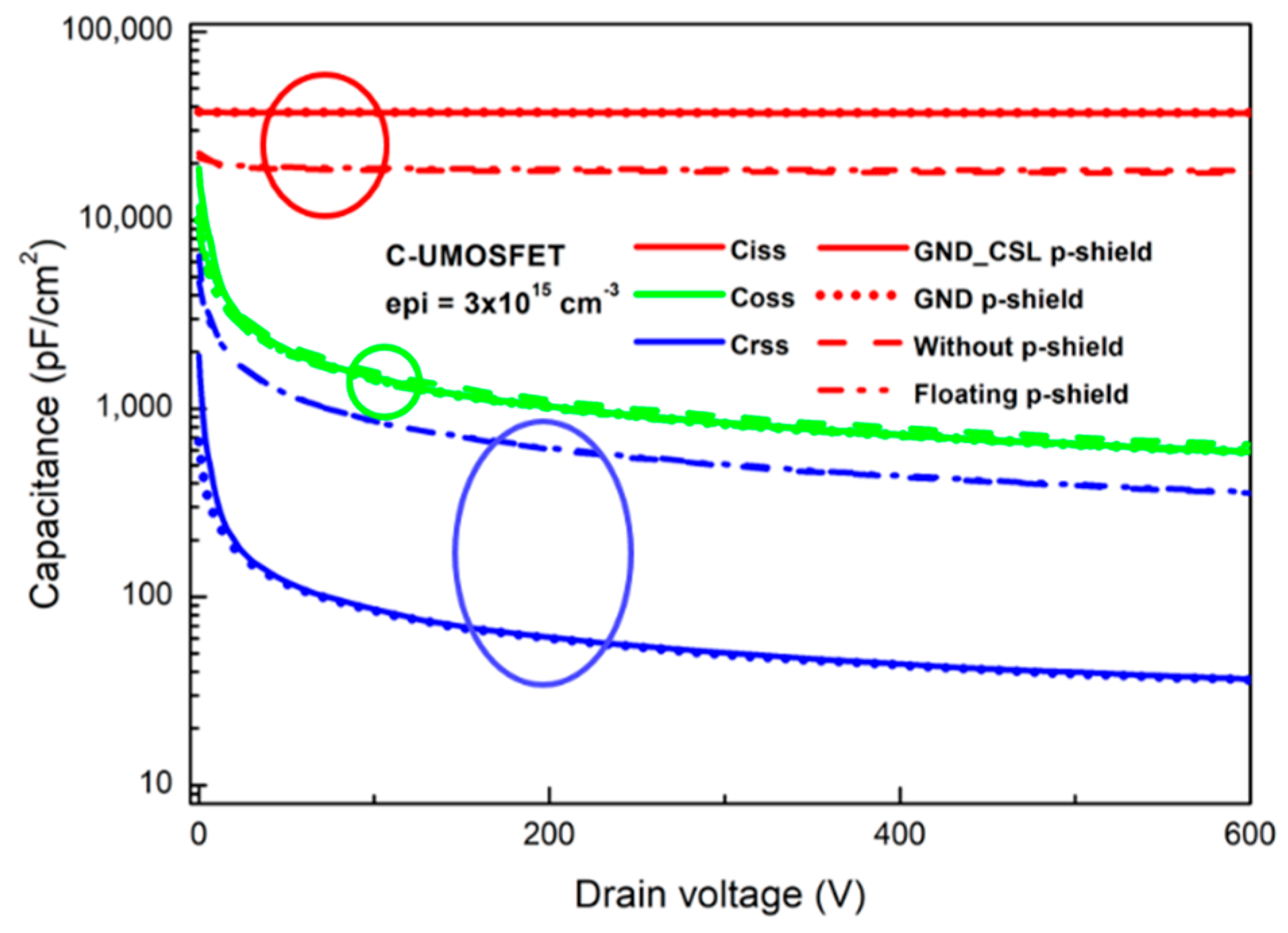
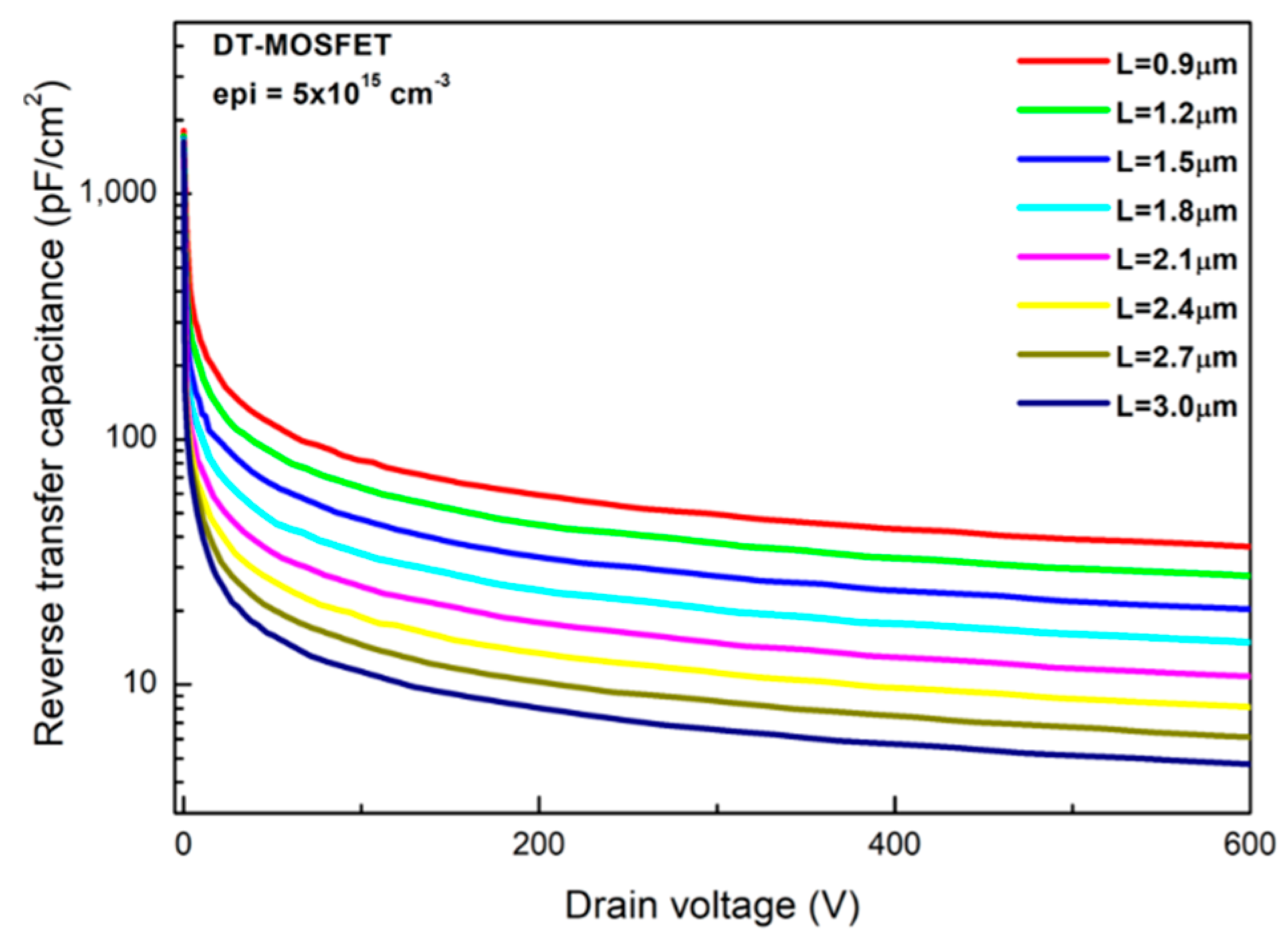
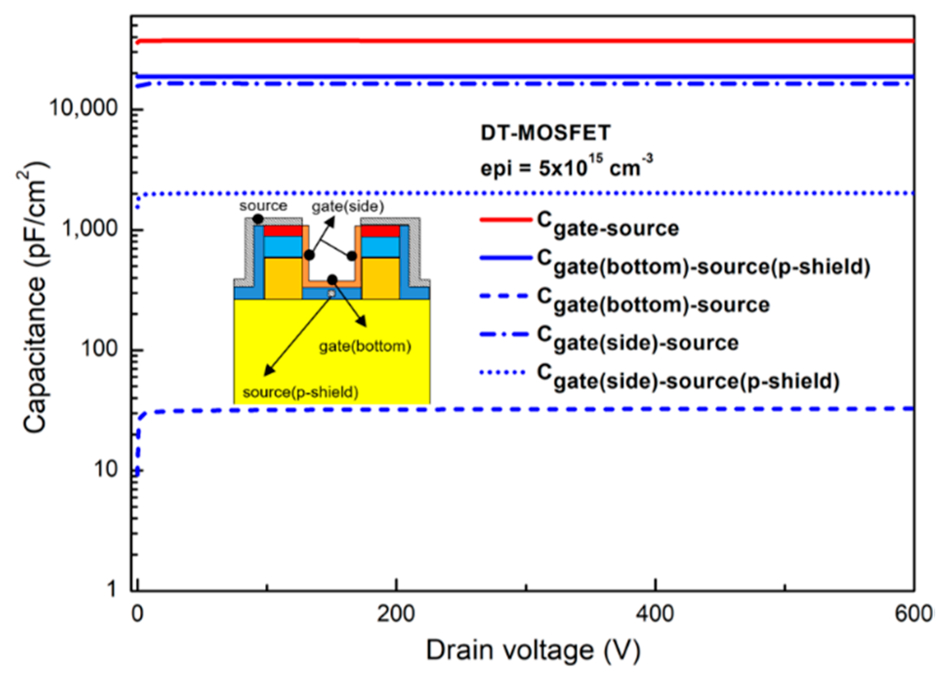
3.2. Terminal Capacitance Characteristics

In this section, the simulation conditions for capacitance extraction are set such that the active area is 1 cm2, the ac small signal is 1 MHz, the gate voltage is fixed at 0 V, and the drain voltage sweeps from 0–600 V. Before analyzing the terminal capacitance of the three structures, the effect of BPR on the capacitance was analyzed. Figure 8 shows the capacitance for both ground and floating BPR and for DSL in the C-UMOSFET. The grounded BPR in contact with the source increases the overlapping area between the gate and the source. Thus, in the case of the grounded BPR, the input capacitance (Ciss:Ciss = CGS + CGD) is higher than that when no BPR is used or when a floating BPR is applied. However, the floating BPR causes dynamic degradation due to its charge storage mechanism [38], and when no BPR is applied to the C-UMOSFET, there is increased degradation of the dynamic characteristics due to hot hole injections that arise from the high electric field in the gate oxide [24]. On the other hand, in the case of grounded BPR, Crss, which plays the most important role in switching energy loss, is effectively reduced. The grounded BPR blocks the electric field between the bottom gate and the drain and screens the charge coupling [38]. Therefore, only the capacitance between the side gate oxide and the drain contributes to the Crss [12]. When the DSL is added, the Crss is nearly identical as when the ground BPR is applied, excluding a slight increase at low drain voltages.
In the UMOSFET structure, the gate-drain capacitance (CGD or Crss) is the series connection between the gate oxide capacitance and the depletion capacitance. According to a previous study on the modeling of gate-drain capacitance in UMOSFET structures, the equation for CGD is as follows [39,40]:
C G D = ( t W + 2 t D t c e l l ) [ C G O X C D C G O X + C D ]
where t’D is the trench depth not overlapping the p-base region, tW is the trench width, tcell is the cell pitch, Cox is the gate oxide capacitance, and CD is the depletion capacitance. However, in the case of a structure in which the source region is trenched, such as DT-MOSFETs and ST-MOSFETs, it is difficult to intuitively analyze the CGD due to the geometric complexity of the structure. Recently, X. Luo et al. [40] illustrated that the CGD operates as a serial connection between the gate-source capacitance and the drain-source capacitance. The gate-drain capacitance equation in Double Trench MOSFET Structure (without BPR) claimed in his paper are:
C G D   =   ( C G S 1 + C D S 1 ) 1 + C G D , b o t t o m
where CGS is the gate-source capacitance, CDS is the drain-source capacitance and CGD,bottom is the gate bottom-drain capacitance. In DT-MOSFET with BPR, CGD,bottom is negligible, so CGD = (CGS−1 + CDS−1)−1. However, this mechanism may contradict the results shown in Figure 9. Figure 9 plots the CGD as function of the trench depth of the source region in the DT-MOSFET. In Figure 9, CGD decreases as L (source trench depth) increases. When L increases, the overlapping area between the gate and the source increases. As such, CGS increases and at the same time, the distance between the drain and the source decreases, leading to an increase in CDS. So, according to (2), as L increases, CGD should increase. This contradicts the simulation results in Figure 9, where CGD decreases as L increases.
Figure 10 shows the capacitance distribution of the three structures. Depletion capacitance is considered to be the serial connection of the JFET capacitance (CJFET) and the Drift capacitance (CDrift). The modified gate-drain capacitance equation is given follows:
C G D = ( C O X 1 + C J F E T 1 + C D r i f t 1 ) 1
Using this model, the capacitance of the trench MOSFET can be analyzed intuitively. First, the gate oxide thickness of the three structures is the same, so Cox is the same. Before the depletion region is fully extended to the drift region, at a low drain voltage, the depletion regions of the DT-MOSFET and ST-MOSFET extend further than that of the C-UMOSFET due to their trenched source regions. Therefore, the CDrift of DT-MOSFET and ST-MOSFET is smaller than that of C-UMOSFET. Indeed, the DT-MOSFET has the smallest CDrift of the three structures because its depletion region is wider than that of the ST-MOSFET due to the P-shielding region below the source region. In the case of the CJFET, it is proportional to the JFET width. The charge in the JFET region is proportional to the JFET width, and the CJFET is proportional to the charge in the JFET region. Therefore, CJFET is smallest in DT-MOSFET and largest in C-UMOSFET. In addition, at a high drain voltage, the drift region is fully depleted and the CDrift of the three structure is nearly the same. Thus, CGD is determined by the CJFET.
Figure 11 plots the terminal capacitance of the three structures. In Figure 11a, the Ciss of the three structures are almost the same. In the DT-MOSFET and ST-MOSFET, the trenched source region for improving the static characteristics increases the overlapping area between the gate and the source. However, as shown in Figure 12, the capacitance between the bottom gate and the BPR is the largest of all CGS components, and BPR is applied to all three structures, so the Ciss of the three structures is not significantly different. The output capacitance (Coss:Coss= CDS + CGD), which depends on the distance between the drain and source, is also not significantly different, though the C-UMOSFET has the smallest COSS. In the case of Crss, according to the previous analysis, the Crss of the DT-MOSFET is the smallest, and the Crss of the C-UMOSFET is the largest. At VD = 600 V, the Crss of DT-MOSFET and ST-MOSFET decreases by 44% and 24%, respectively, compared to the value of C-UMOSFET. The capacitance simulation results for each structure are shown in Table 3.

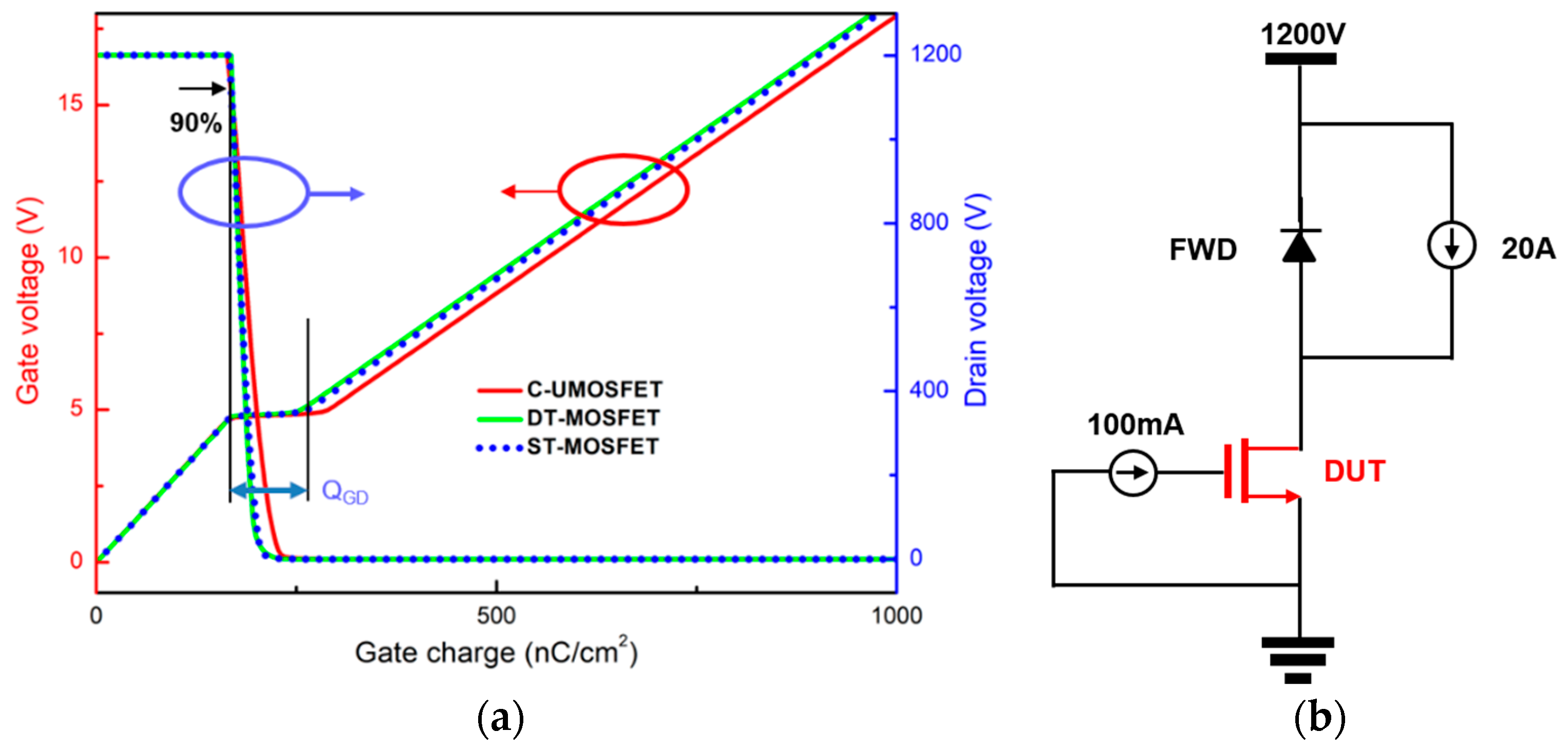
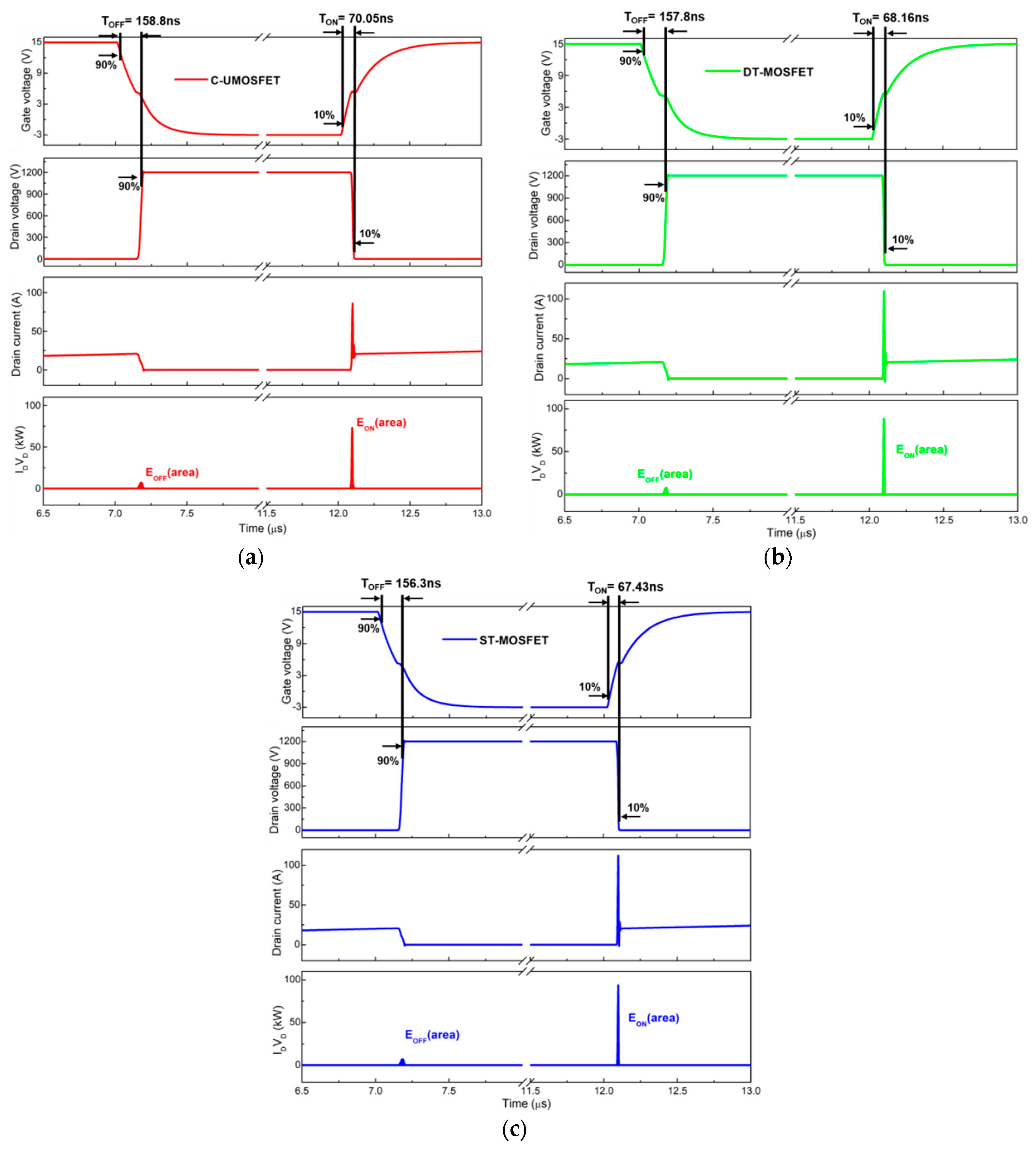
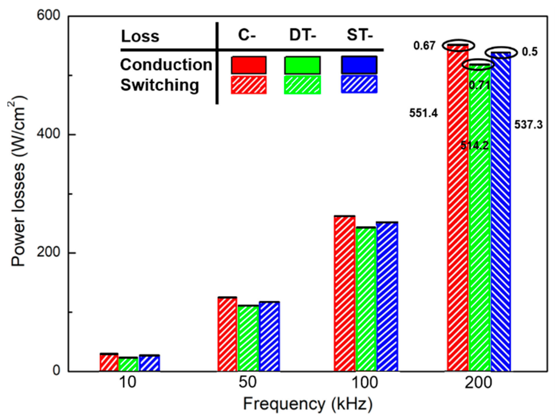
3.3. Dynamic Charateristics

Figure 13a shows the gate charge curves of the three structures. The test circuit is shown in Figure 13b and a constant current of 100 mA is used to charge the gate. The active area of the device under test (DUT) for gate charge simulation was set to 1 cm2. In addition, test conditions were set so that the supplying voltage (VDD) was 1200 V and the load current (ID) was 20 A. The gate-drain charge (QGD or Miller plateau) is one of the key parameters that can determine the switching speed of the device and is dependent on CGD. The extracted QGD values are 114.8 nC/cm2, 80.6 nC/cm2, 89.2 nC/cm2 for C-UMOSFET, DT-MOSFET, and ST-MOSFET, respectively. In addition, the extracted total gate charge (QG) values are 839 nC/cm2, 805.1 nC/cm2, 812.7 nC/cm2 for C-UMOSFET, DT-UMOSFET, and ST-UMOSFET. This result is proportional to the extracted results of CGD. The HF-FOM (RON-SP × QGD) of DT-MOSFET and ST-MOSFET is 289 mΩ∙nC, 224 mΩ∙nC, respectively, which is improved by 26% and 42% compared to C-UMOSFET.
Table 3 summarizes the results including the values for terminal capacitance, gate charge, and HF-FOMs, which are significant parameters for high frequency performance [8,37,41].
Finally, the switching performance parameter of the device was extracted through a double-pulse test (DPT). The active areas of all the DUT were set to 0.3 cm2 [42], which is similar to that of commercial devices [43]. Figure 14a plots the full waveform of the ST-MOSFET. Figure 14b shows the test circuit in the three structures. The gate resistance is set to 10 Ω, and the gate voltage switched between 15 V and −3 V for the on- and off-states. The stray inductance was assumed to be 10 nH. The load inductance was set to 300 μH, and the first gate voltage pulse lasted 5 μs so that the load current flow was 20 A. The body diode of the same device as the DUT was used as a freewheeling diode, and the supply voltage was 1200 V.
In this paper, turn-on time (TON) and turn-off time (TOFF) are defined as follows [43,44,45].
T O N = T D O N + T R
T O F F = T D O F F + T F
where TD-ON is the turn-on delay time (from 10% of VG to 90% of VD at the rising edge), TR is the rise time at the turn-on transient (from 90% of VD to 10% of VD at the rising edge), TD-OFF is the turn-off delay time (from 90% of VG to 10% of VD at the falling edge) and fall time at the turn-off transient (from 10% of VD to 90% of VD at the falling edge). Figure 15 shows the switching waveforms of each structure, and Table 4 summarizes the detailed switching performance data. The switching speed (TON and TOFF) of the device is most affected by Ciss, and TR and TF are most dependent on CGD [37,41]. In hard switching, VD and ID are swept during TR and TF, so energy loss is dependent upon TR and TF. In the previous section, we observed that the Ciss of DT-MOSFET and ST-MOSFET is almost the same as the value of C-UMOSFET. Therefore, the switching speed of DT-MOSFET and ST-MOSFET is maintained at the same level as C-UMOSFET. In addition, the CGD of DT-MOSFET and ST-MOSFET is superior to that of C-UMOSFET, which improves the switching energy loss. The switching energy loss of C-UMOSFET, DT-MOSFET, and ST-MOSFET are 827.1 μJ, 771.2 μJ, and 806 μJ, respectively. In addition, since the drain voltage sweeps from low to high at the falling edge of the turn-off transient, TOFF is relatively slower than TON. Moreover, since the body diode of each device was used as FWD, EON includes the diode reverse recovery. Therefore, EON is relatively larger than EOFF.
The total power losses Pt of the device consist of conduction losses and switching losses and are calculated as follows [19,37,40]:
P t = d R o n s p I d 2 + f ( E O N + E O F F )
where d is the duty cycle and f is the switching frequency. Figure 16 shows the power losses which vary with the switching frequency when the duty cycle is 0.5. As the switching frequency increases, the ratio of switching losses of total power losses increases. The power losses of C-UMOSFET, DT-MOSFET, and ST-MOSFET when operating at 200 kHz are 552.1 W/cm2, 514.9 W/cm2 and 537.8 W/cm2, respectively.

4. Conclusions

In this paper, the static and dynamic performance of the 4H-SiC C-UMOSFET, DT-MOSFET and ST-MOSFET were compared through TCAD simulation. In static characteristics, the RON-SP of the ST-MOSFET is 2.52 mΩ∙cm2, which is 25% lower than that of C-UMOSFET. Furthermore, the DC-FOM of the ST-MOSFET is 1179 MW/cm2, which is 37% higher than that of the C-UMOSFET. At VD = 1200 V, the Eox-max of the DT-MOSFET is 0.6 MV/cm, which was 44% lower than that of the C-UMOSFET. To improve the static characteristics, both the DT-MOSFET and ST-MOSFET are trenched in the source region. For the same reason, the BPR is introduced in the three structures. The effect of the trenched source region and BPR on the capacitance was analyzed, and the dynamic characteristics of the three structures were compared. Due to the trenched source region, the overlapping area between the gate and source increases. Nevertheless, the capacitance between the gate and the BPR is largest of CGS components, so the Ciss is almost identical in all three structure. On the other hand, the CGD of DT-MOSFET and ST-MOSFET is reduced by 44% and 24%, respectively, compared to C-UMOSFET. This is because the depletion region is expanded by the trenched source region. Since the CGD of DT-MOSFET and ST-MOSFET is superior to that of C-UMOSFET, it improves HF-FOM (RON-SP × CGD). The HF-FOM (RON-SP × QGD) of DT-MOSFET and ST-MOSFET is 289 mΩ∙nC, 224 mΩ∙nC, respectively, which is improved by 26% and 42% compared to C-UMOSFET. The switching speed of DT-MOSFET and ST-MOSFET are maintained at the same level as the C-UMOSFET. The switching energy loss and power loss of the DT-MOSFET and ST-MOSFET are slightly improved compared to C-UMOSFET.

Author Contributions

All authors contributed to this work. Investigation, J.C., K.K.; Methodology, J.C., K.K.; Supervision, J.C., K.K.; Writing—original draft, J.C.; Writing-review and editing, K.K. All authors have read and agreed to the published version of the manuscript.

Funding

This research received no external funding.

Acknowledgments

This research was supported by Samsung Electronics, the MSIT (Ministry of Science and ICT), Korea, under the ITRC (Information Technology Research Center) support program (IITP-2020-2018-0-01421) supervised by the IITP (Institute for Information & communications Technology Promotion), and then the IDEC (IC Design Education Center).

Conflicts of Interest

The authors declare no conflict of interest.

References

  1. Zhang, M.; Wei, J.; Jiang, H.; Chen, K.J.; Cheng, C.H. A new SiC trench MOSFET structure with protruded p-base for low oxide field and enhanced switching performance. IEEE Trans. Device Mater. Rel. 2017, 17, 432–437. [Google Scholar] [CrossRef]
  2. Cooper, J.A.; Agarwal, A. SiC power-switching devices—The second electronics revolution? Proc. IEEE 2002, 90, 956–968. [Google Scholar] [CrossRef]
  3. Ebihara, Y.; Ichimura, A.; Mitani, A.; Noborio, M.; Takeuchi, Y.; Mizuno, S.; Yamamoto, T.; Tsuruta, K. Deep-P Encapsulated 4HSiC Trench MOSFETs With Ultra Low RonQgd. In Proceedings of the IEEE 30th International Symposium on Power Semiconductor Devices and ICs (ISPSD), Chicago, IL, USA, 13–17 May 2018; pp. 44–48. [Google Scholar]
  4. Cooper, J.; Melloch, M.; Singh, R.; Agarwal, A.; Palmour, J. Status and prospects for SiC power MOSFETs. IEEE Trans. Electron Devices 2002, 49, 658–664. [Google Scholar] [CrossRef]
  5. Yano, H.; Nakao, H.; Hatayama, T.; Uraoka, Y.; Fuyuki, T. Increased Channel Mobility in 4H-SiC UMOSFETs Using On-Axis Substrates. Mater. Sci. Forum 2007, 556–557, 807–810. [Google Scholar] [CrossRef]
  6. Banzhaf, C.T.; Grieb, M.; Trautmann, A.; Bauer, A.J.; Frey, L. Characterization of Diverse Gate Oxides on 4H-SiC 3D Trench-MOS Structures. Mater. Sci. Forum 2013, 740, 691–694. [Google Scholar] [CrossRef]
  7. Kojima, T.; Harada, S.; Kobayashi, Y.; Sometani, M.; Ariyoshi, K.; Senzaki, J.; Takei, M.; Tanaka, Y.; Okumura, H. Self-aligned formation of the trench bottom shielding region in 4H-SiC trench gate MOSFET. Jpn. J. Appl. Phys. 2016, 55, 04ER02. [Google Scholar] [CrossRef]
  8. Vudumula, P.; Kotamraju, S. Design and Optimization of 1.2-kV SiC Planar Inversion MOSFET Using Split Dummy Gate Concept for High-Frequency Applications. IEEE Trans. Electron Devices 2019, 66, 5266–5271. [Google Scholar] [CrossRef]
  9. Agarwal, A.K.; Siergiej, R.R.; Seshadri, S.; White, M.H.; McMullin, P.G.; Burk, A.A.; Rowland, L.B.; Brandt, C.D.; Hopkins, R.H. A critical look at the performance advantages and limitations of 4H-SiC power UMOSFET structures. In Proceedings of the 8th International Symposium on Power Semiconductor Devices and ICs, Maui, HI, USA, 23 May 1996; pp. 119–122. [Google Scholar]
  10. Singh, R.; Hefner, A.R. Reliability of SiC MOS devices. Solid State Electron. 2004, 48, 1717–1720. [Google Scholar] [CrossRef]
  11. Siemieniec, R.; Peters, D.; Esteve, R.; Bergner, W.; Basler, T.; Zippelius, B.; Kuck, D.; Aichinger, T. A SiC Trench MOSFET concept offering improved channel mobility and high reliability. In Proceedings of the 19th European Conference on Power Electronics and Applications (EPE’17 ECCE Europe), Warsaw, Poland, 11–14 September 2017; pp. P.1–P.13. [Google Scholar]
  12. Kagawa, Y.; Fujiwara, N.; Sugawara, K.; Tanaka, R.; Fukui, Y.; Yamamoto, Y.; Miura, N.; Imaizumi, M.; Nakata, S.; Yamakawa, S. 4H-SiC Trench MOSFET with Bottom Oxide Protection. Mater. Sci. Forum 2014, 778–780, 919–922. [Google Scholar] [CrossRef]
  13. Kobayashi, Y.; Kinoshita, A.; Onishi, Y. Simulation Based Prediction of SiC Trench MOSFET Characteristics. FUJI Elect. Rev. 2016, 62, 12–16. [Google Scholar]
  14. Baliga, B.J. Silicon Carbide Power Devices; World Scientific: Singapore, 2006; pp. 339–358. [Google Scholar]
  15. Li, Y.; Cooper, J.; Capano, M. High-voltage (3 kV) UMOSFETs in 4H-SiC. IEEE Trans. Electron Devices 2002, 49, 972–975. [Google Scholar] [CrossRef]
  16. Yang, T.; Bai, S.; Huang, R. 4H-SiC trench MOSFET with splitting double-stacked shielded region. Superlattices Microstruct. 2018, 122, 419–425. [Google Scholar] [CrossRef]
  17. Wei, J.; Zhang, M.; Jiang, H.; Cheng, C.-H.; Chen, K.J. Low ON-Resistance SiC Trench/Planar MOSFET With Reduced OFF-State Oxide Field and Low Gate Charges. IEEE Electron Device Lett. 2016, 37, 1458–1461. [Google Scholar] [CrossRef]
  18. Jiang, H.; Wei, J.; Dai, X.; Ke, M.; Deviny, I.; Mawby, P. SiC Trench MOSFET With Shielded Fin-Shaped Gate to Reduce Oxide Field and Switching Loss. IEEE Electron Device Lett. 2016, 37, 1324–1327. [Google Scholar] [CrossRef]
  19. Zhou, X.; Yue, R.; Zhang, J.; Dai, G.; Li, J.; Wang, Y. 4H-SiC trench MOSFET with floating/grounded junction barrier-controlled gate structure. IEEE Trans. Electron Devices 2017, 64, 4568–4574. [Google Scholar] [CrossRef]
  20. Peters, D.; Basler, T.; Zippelius, B.; Aichinger, T.; Bergner, W.; Esteve, R.; Kueck, D.; Siemieniec, R. The new CoolSiC™ Trench MOSFET Technology for Low Gate Oxide Stress and High Performance. In Proceedings of the International Exhibition and Conference for Power Electronics, Intelligent Motion, Renewable Energy and Energy Management, Nuremberg, Germany, 16–18 May 2017; pp. 168–174. [Google Scholar]
  21. Peters, D.; Siemieniec, R.; Aichinger, T.; Basler, T.; Esteve, R.; Bergner, W.; Kueck, D. Performance and ruggedness of 1200V SiC Trench MOSFET. In Proceedings of the 29th International Symposium on Power Semiconductor Devices and IC’s (ISPSD), Sapporo, Japan, 28 May–1 June 2017; pp. 239–242. [Google Scholar]
  22. Nakamura, T.; Nakano, Y.; Aketa, M.; Mitani, S.; Sakairi, H.; Yokotsuji, Y. High performance SiC trench devices with ultra-low Ron. In Proceedings of the International Electron Devices Meeting, Washington, DC, USA, 5–7 December 2011; pp. 26.5.1–26.5.3. [Google Scholar]
  23. Sampath, M.; Morisette, D.; Cooper, J.A. Comparison of singleand double-trench UMOSFETs in 4H-SiC. In Materials Science Forum; Trans Tech Publications Ltd.: Freienbach, Switzerland, 2018; Volume 924, pp. 752–755. [Google Scholar]
  24. Wei, J.; Liu, S.; Yang, L.; Tang, L.; Lou, R.; Li, T.; Fang, J.; Li, S.; Zhang, C.; Sun, W. Investigations on the Degradations of Double-Trench SiC Power MOSFETs Under Repetitive Avalanche Stress. IEEE Trans. Electron Devices 2018, 66, 546–552. [Google Scholar] [CrossRef]
  25. Kyogoku, S.; Tanaka, K.; Ariyoshi, K.; Iijima, R.; Kobayashi, Y.; Harada, S. Role of Trench Bottom Shielding Region on Switching Characteristics of 4H-SiC Double-Trench Mosfets. Mater. Sci. Forum 2018, 924, 748–751. [Google Scholar] [CrossRef]
  26. Kim, T.; Kim, K. High Breakdown Voltage and Low On-Resistance 4H-SiC UMOSFET with Source-Trench Optimization. ECS J. Solid State Sci. Technol. 2019, 8, Q147–Q152. [Google Scholar] [CrossRef]
  27. Kobayashi, Y.; Harada, S.; Ishimori, H.; Takasu, S.; Kojima, T.; Ariyoshi, K.; Sometani, M.; Senzaki, J.; Takei, M.; Tanaka, Y.; et al. 3.3 kV-Class 4H-SiC UMOSFET by Double-Trench with Tilt Angle Ion Implantation. Mater. Sci. Forum 2016, 858, 974–977. [Google Scholar] [CrossRef]
  28. Jiang, J.-Y.; Wu, T.-L.; Zhao, F.; Huang, C.-F. Numerical Study of 4H-SiC UMOSFETs with Split-Gate and P+ Shielding. Energies 2020, 13, 1122. [Google Scholar] [CrossRef] [Green Version]
  29. Saha, A.; Cooper, J.A. A 1-kV 4H-SiC Power DMOSFET Optimized for Low on-Resistance. IEEE Trans. Electron Devices 2007, 54, 2786–2791. [Google Scholar] [CrossRef]
  30. Synopsys Inc. Sentaurus Device, User Manual, Version O-2018.06; Synopsys Inc.: Mountain View, CA, USA, 2018. [Google Scholar]
  31. Lombardi, C.; Manzini, S.; Saporito, A.; Vanzi, M. A physically based mobility model for numerical simulation of nonplanar devices. IEEE Trans. Comput. Des. Integr. Circuits Syst. 1988, 7, 1164–1171. [Google Scholar] [CrossRef]
  32. Hatakeyama, T.; Nishio, J.; Ota, C.; Shinohe, T. Physical modeling and scaling properties of 4H-SiC power devices. In Proceedings of the International Conference On Simulation of Semiconductor Processes and Devices, Tokyo, Japan, 1–3 September 2005; pp. 171–174. [Google Scholar]
  33. Zhao, Y.; Niwa, H.; Kimoto, T. Impact ionization coefficients of 4H-SiC in a wide temperature range. Jpn. J. Appl. Phys. 2018, 58, 018001. [Google Scholar] [CrossRef]
  34. Kang, H.; Udrea, F. On the Quasi-Saturation in State-of-the-Art Power MOSFETs. IEEE Electron Device Lett. 2019, 40, 754–756. [Google Scholar] [CrossRef]
  35. Goh, J.; Kim, K. Low on-resistance 4H-SiC UMOSFET with local floating superjunction. J. Comput. Electron. 2019, 19, 234–241. [Google Scholar] [CrossRef]
  36. Dimarino, C.; Chen, Z.; Danilovic, M.; Boroyevich, D.; Burgos, R.; Mattavelli, P. High-temperature characterization and comparison of 1.2 kV SiC power MOSFETs. In Proceedings of the IEEE Energy Conversion Congress and Exposition, Denver, CO, USA, 15–19 September 2013; pp. 3235–3242. [Google Scholar] [CrossRef]
  37. Baliga, B.J. Fundamentals of Power Semiconductor Devices; Springer: Berlin, Germany, 2008; pp. 279–497. [Google Scholar]
  38. Wei, J.; Zhang, M.; Jiang, H.; Wang, H.; Chen, K.J. Dynamic Degradation in SiC Trench MOSFET With a Floating p-Shield Revealed with Numerical Simulations. IEEE Trans. Electron Devices 2017, 64, 2592–2598. [Google Scholar] [CrossRef]
  39. Alatise, O.; Parker-Allotey, N.-A.; Jennings, M.; Mawby, P.; Kennedy, I.; Petkos, G. Modeling the Impact of the Trench Depth on the Gate–Drain Capacitance in Power MOSFETs. IEEE Electron Device Lett. 2011, 32, 1269–1271. [Google Scholar] [CrossRef] [Green Version]
  40. Luo, X.; Liao, T.; Wei, J.; Fang, J.; Yang, F.; Zhang, B. A novel 4H-SiC trench MOSFET with double shielding structures and ultralow gate-drain charge. J. Semicond. 2019, 40, 052803. [Google Scholar] [CrossRef]
  41. Han, K.J.; Baliga, B.J.; Sung, W. A Novel 1.2 kV 4H-SiC Buffered-Gate (BG) MOSFET: Analysis and Experimental Results. IEEE Electron Device Lett. 2017, 39, 248–251. [Google Scholar] [CrossRef]
  42. Zhang, J.; Rees, F.L.; Hull, B.; Casady, J.B.; Allen, S.; Palmour, J.W. Impact of next-generation 1700V SiC MOSFETs in a 125kW PV converter. In Proceedings of the IEEE Energy Conversion Congress and Exposition (ECCE), Cincinnati, OH, USA, 1–5 October 2017; pp. 911–916. [Google Scholar]
  43. Tian, K.; Hallen, A.; Qi, J.; Ma, S.; Fei, X.; Zhang, A.; Liu, W. An Improved 4H-SiC Trench-Gate MOSFET With Low ON-Resistance and Switching Loss. IEEE Trans. Electron Devices 2019, 66, 2307–2313. [Google Scholar] [CrossRef]
  44. Graovac, D.; Purschel, M.; Kiep, A. MOSFET power losses calculation using the data-sheet parameters application note, v1.1. Infineon Technol. AG 2006, 1, 1–23. [Google Scholar]
  45. Backlund, B.; Schnell, R.; Ulrich, S.; Roland, F. Applying IGBTs; Application Note 5SYA2053-01; ABB: Lenzburg, Switzerland, 2007. [Google Scholar]
Figure 1. Schematic cross-sectional view of (a) C-UMOSFET, (b) DT-MOSFET, and (c) ST-MOSFET.
Electronics 09 01895 g001
Figure 2. Off-state breakdown characteristic cures of each structure.
Electronics 09 01895 g002
Figure 3. Variation of breakdown voltage of each structure with epi-layer doping concentration.
Electronics 09 01895 g003
Figure 4. (a) On-state output characteristic curves in the linear region of each structure with the drain voltage range of 0–25 V and (b) Overall on-state output characteristic curves of each structure with the drain voltage range of 0–800 V.
Electronics 09 01895 g004
Figure 5. Off-state gate oxide electric field distribution of (a) C-UMOSFET, (b) DT-MOSFET, and (c) ST-MOSFET at VD = 1200 V.
Electronics 09 01895 g005
Figure 6. Transfer characteristics of each structure at VD = 20 V.
Electronics 09 01895 g006
Figure 7. (a) Threshold voltage versus temperature of each structure taken at VD = 20 V and ID = 1 A; (b) Specific on-resistance versus temperature of each structure taken at VG = 15 V and ID = 20 A.
Electronics 09 01895 g007
Figure 8. Terminal capacitance of C-UMOSFET. The effect of BPR and DSL on the capacitance is observed.
Electronics 09 01895 g008
Figure 9. Reverse transfer capacitance of DT-MOSFET varying in source trench depth.
Electronics 09 01895 g009
Figure 10. Capacitance distribution for (a) C-UMOSFET, (b) DT-MOSFET, and (c) ST-MOSFET.
Electronics 09 01895 g010
Figure 11. (a) Input capacitance, (b) output capacitance, and (c) reverse transfer capacitance of each structure.
Electronics 09 01895 g011
Figure 12. Gate-source capacitance distribution of DT-MOSFET.
Electronics 09 01895 g012
Figure 13. (a) Gate charge characteristics of each structure; (b) Test circuit.
Electronics 09 01895 g013
Figure 14. (a) Full DPT waveform of ST-MOSFET; (b) Test circuit.
Electronics 09 01895 g014
Figure 15. Switching waveform of (a) C-UMOSFET, (b) DT-MOSFET, and (c) ST-MOSFET.
Electronics 09 01895 g015
Figure 16. Comparison of power losses depending on switching frequency.
Electronics 09 01895 g016
Table 1. Device parameter of each structure.
ParameterC-DT-ST-
Cell pitch (μm)5.555.555.55
Gate-trench width (μm)1.551.551.55
Gate-trench depth (μm)1.51.51.5
P-base width (μm)222
P+ shield width (μm)1.551.551.55
Channel length (μm)0.50.50.5
Gate oxide thickness (μm)0.050.050.05
Epi-layer thickness (μm)181818
P+ shield thickness (μm)0.30.30.3
N-sub thickness (μm)111
Source-trench width (μm)-0.50.5
Source-trench depth (μm)-1.52.4
Source oxide thickness (μm)--0.1
Source doping concentration (cm−3)1 × 10191 × 10191 × 1019
P-base doping concentration (cm−3)1 × 10171 × 10171 × 1017
P+ shield doping concentration (cm−3)5 × 10185 × 10185 × 1018
Epi-layer doping concentration (cm−3)3 × 10155 × 10155 × 1015
N-sub doping concentration (cm−3)1 × 10191 × 10191 × 1019
DSL doping concentration (cm−3)1 × 10161 × 10161 × 1016
Table 2. Static performance of each structure.
ParameterC-DT-ST-
Breakdown voltage [V]169917061724
RON-SP [mΩ∙cm2]3.373.572.52
EOX-MAX (@VG = 0 V, VD = 1200 V) [MV/cm]1.110.620.72
VTH [V]5.745.755.75
DC-FOM (BV2/RON-SP) [MW/cm2]8578151179
Table 3. Dynamic performance of each structure.
ParameterC-DT-ST-
CISS (@VD = 600 V, f = 1 MHz) [nF/cm2]3737.336.2
COSS (@VD = 600 V, f = 1 MHz) [pF/cm2]590763765
CRSS (@VD = 600 V, f = 1 MHz) [pF/cm2]36.520.327.7
QG [nC/cm2]839805813
QGD [nC/cm2]1158189
HF-FOM < RON-SP × QG > [mΩ∙nC]282728742049
HF-FOM < RON-SP × QGD > [mΩ∙nC]388289224
Table 4. Switching performance of each structure.
ParameterC-DT-ST-
TD-ON [ns]56.8757.6856.70
TR [ns]13.1810.4810.73
TON [ns]70.0568.1667.43
TD-OFF [ns]135.1137.4132.7
TF [ns]23.7520.4823.53
TOFF [ns]158.8157.8156.3
EON [μJ]655.3610.7637.5
EOFF [μJ]171.8160.6168.5
ESW [μJ]827.1771.2806.0
Publisher’s Note: MDPI stays neutral with regard to jurisdictional claims in published maps and institutional affiliations.

