A Novel Non-Isolated Three-Port Bidirectional DC/DC Converter for Photovoltaic Electric Scooter Charging Stations


Abstract
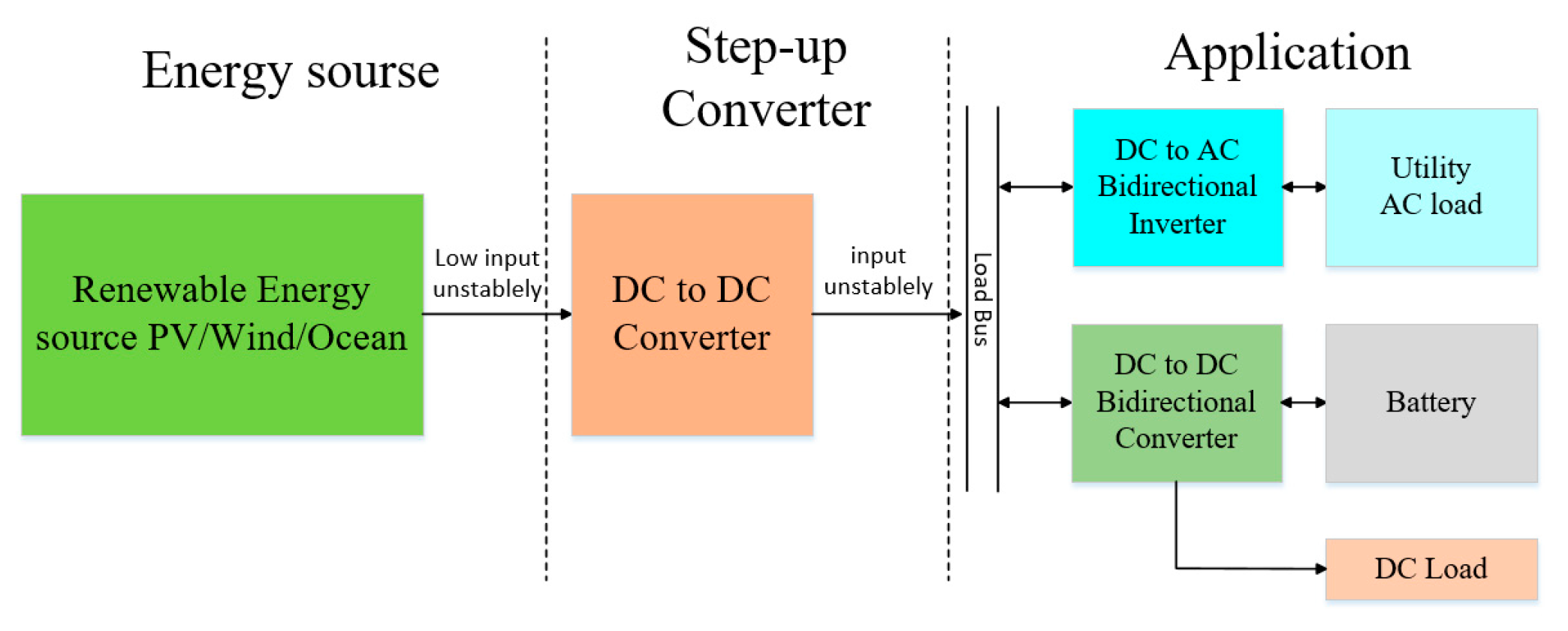
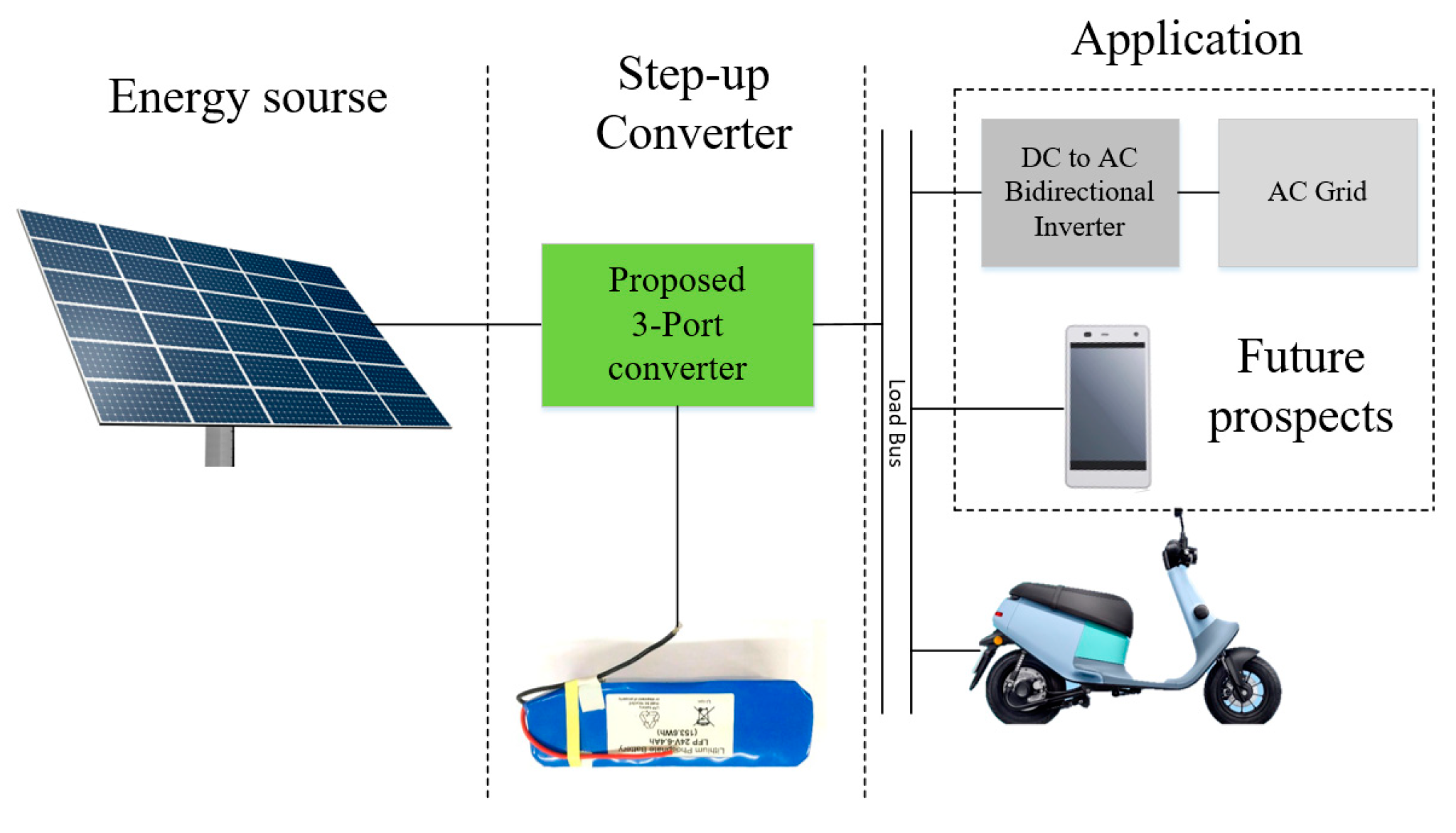
1. Introduction
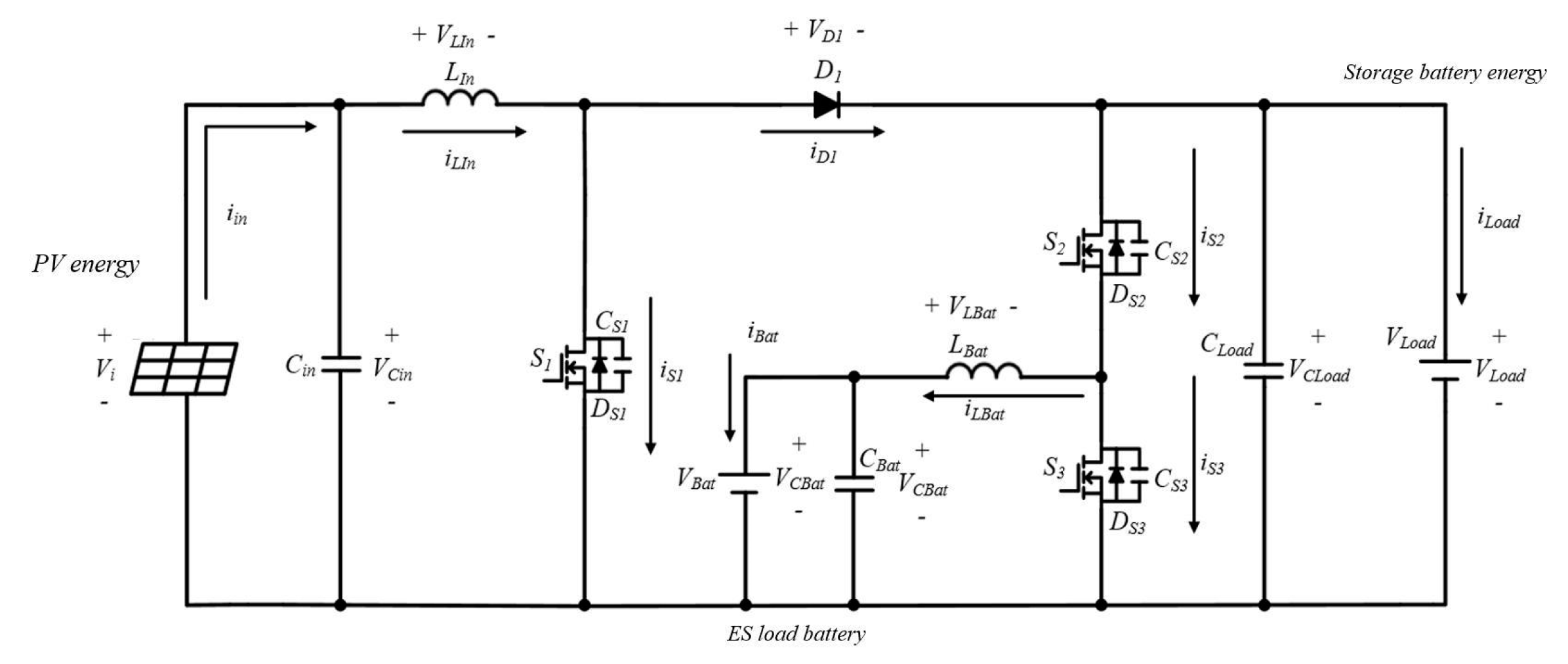
2. Proposed Converter and Operating Principles
- (1)
- The capacitance levels of Cin, CLoad, and CBat are sufficiently high, and the output voltage can be maintained as a constant voltage source.
- (2)
- All switches S1, S2, and S3 and diode D1 are ideal components.
- (3)
- The inductor current is in continuous mode (maintains a positive value).
- (4)
- The switching period is T, the turned-on time of the switches is DT, and the turned-off time of the switches is 1 − DT.
- A.
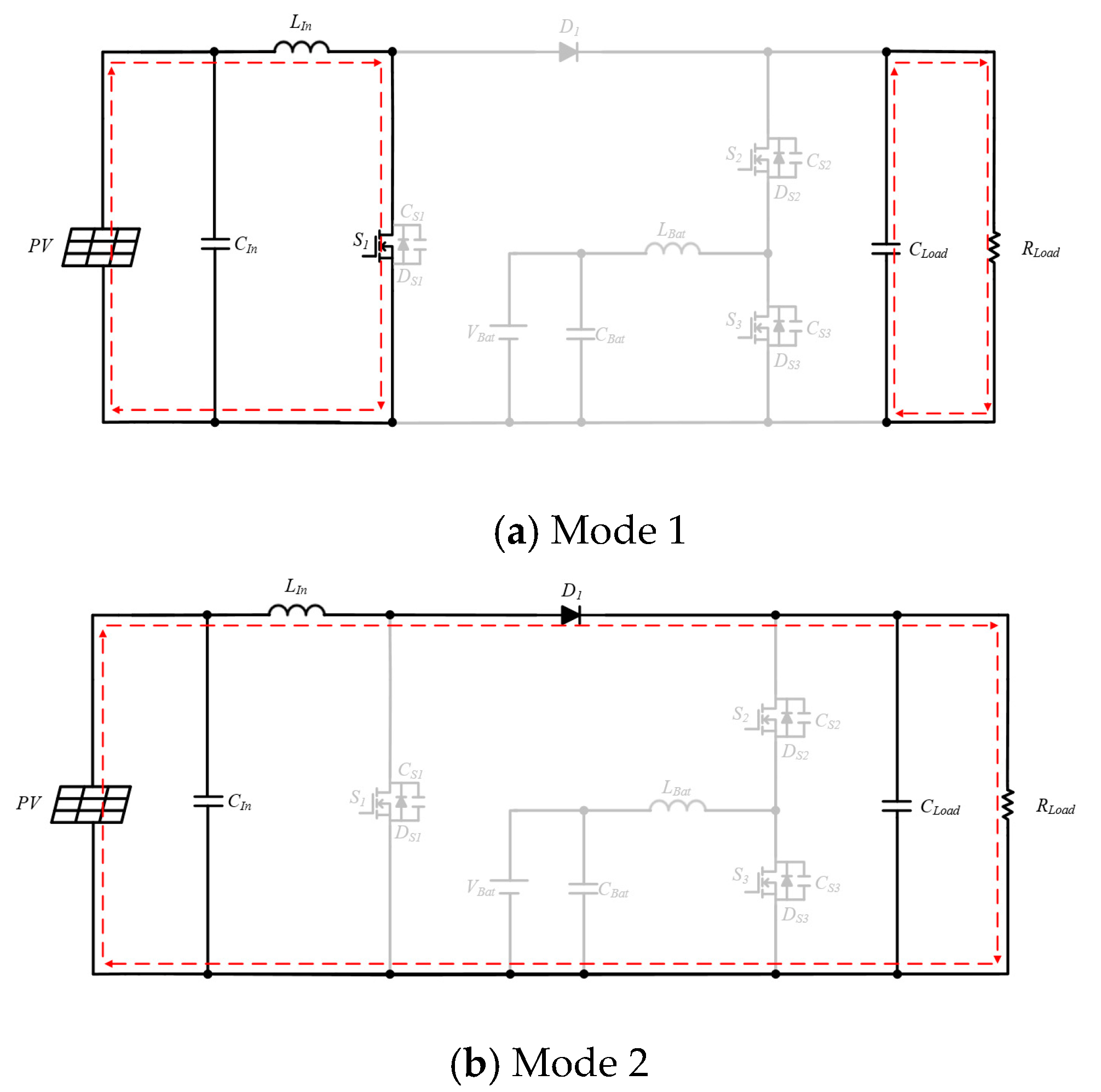
- Stage 1: The PV output voltage is stepped up to the ES bus to charge the ES battery
- a.
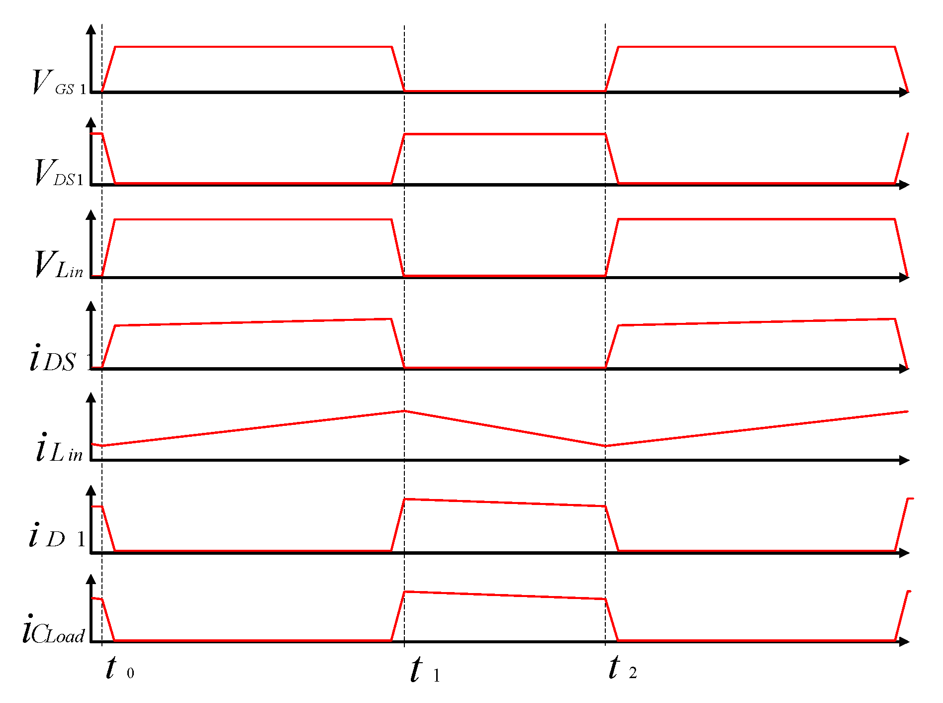
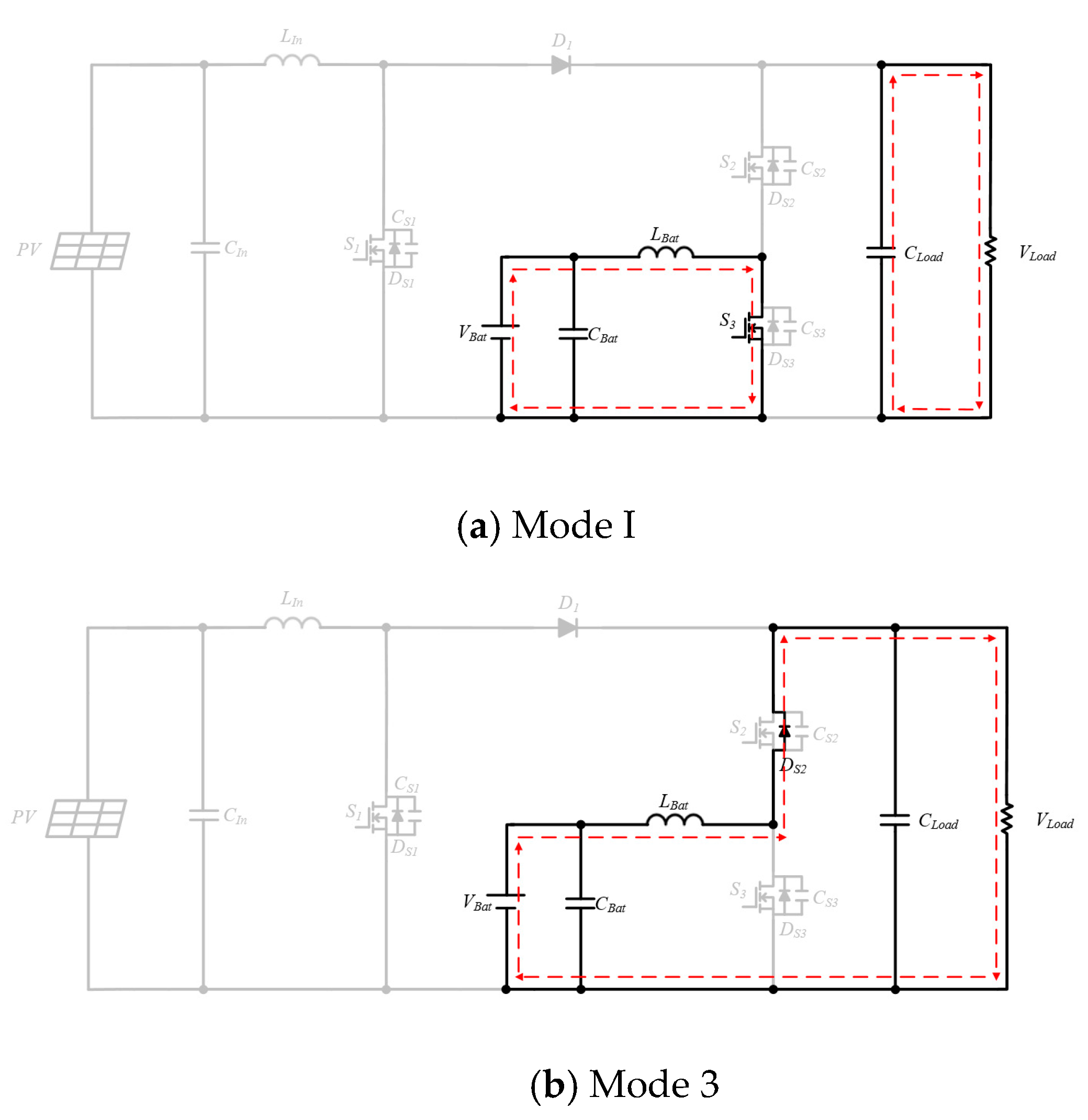
- Mode 1 [t0 ≤ t < t1]
- b.
- Mode 2 [t1 ≤ t < t2]
- B.
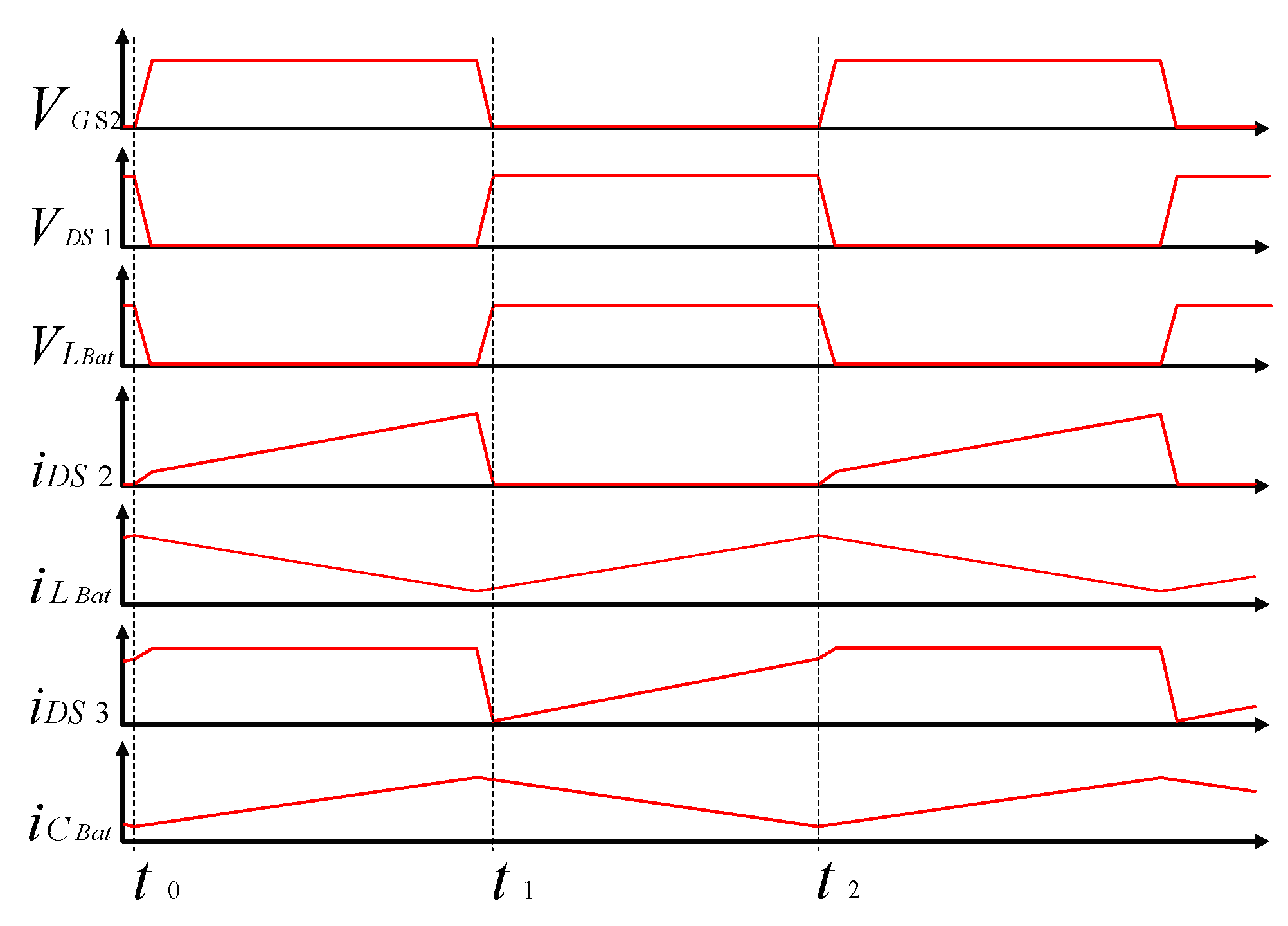
- Stage 2: ES bus is stepped down to charge storage battery
- a.
- Mode 1 [t0 ≤ t < t1]
- b.
- Mode 2 [t1 ≤ t < t2]
- C.
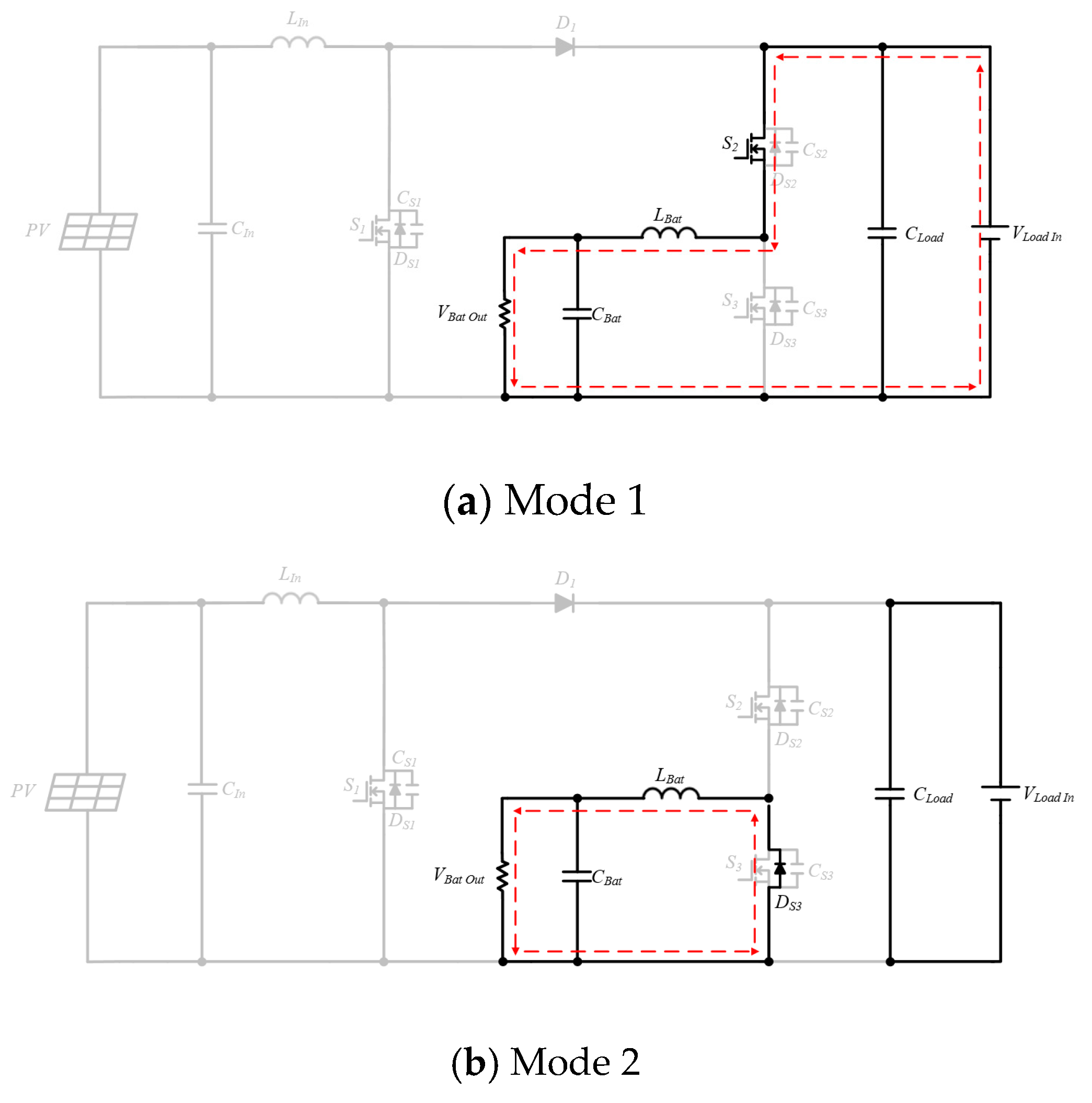
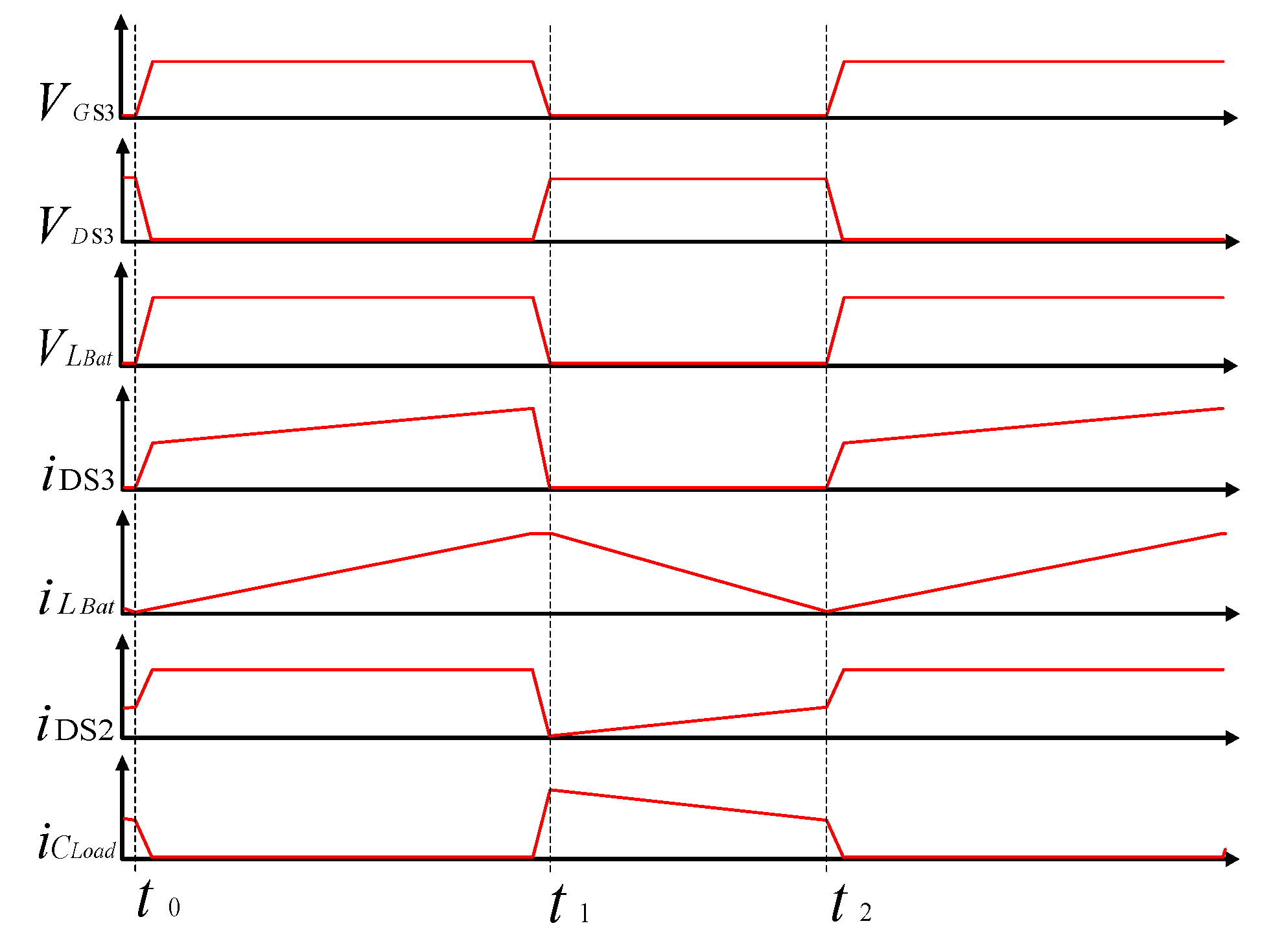
- Stage 3: Storage battery provides energy to ES bus and charge the ES battery
- a.
- Mode 1 [t0 ≤ t < t1]
- b.
- Mode 2 [t1 ≤ t < t2]
3. Operation Mode Conversion Analysis
4. Steady-State Analysis
- (1)
- All components in the proposed topology are ideal components.
- (2)
- The capacitance is sufficiently large to maintain a constant voltage.
- (3)
- The system operates in a continuous conduction mode.
4.1. Voltage Conversion Ratio
4.2. Voltage Stress of Components
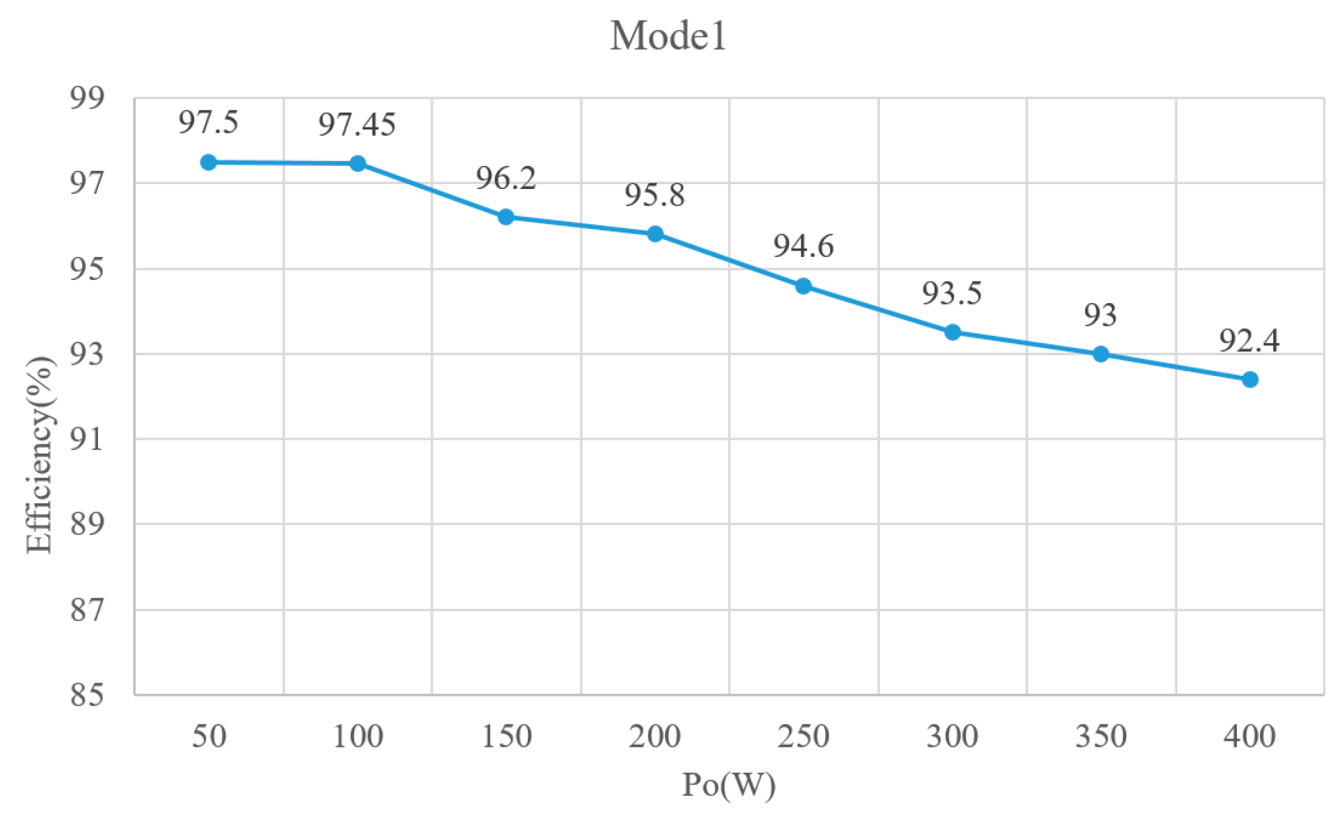
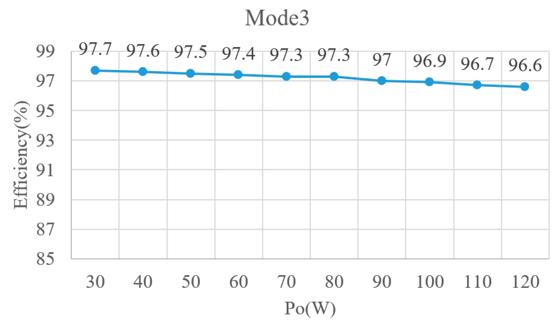
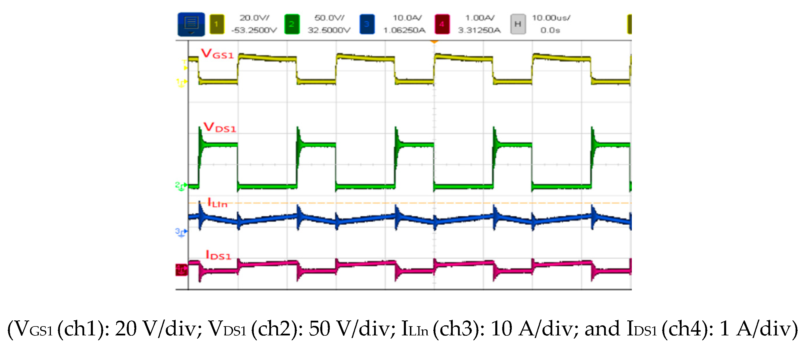
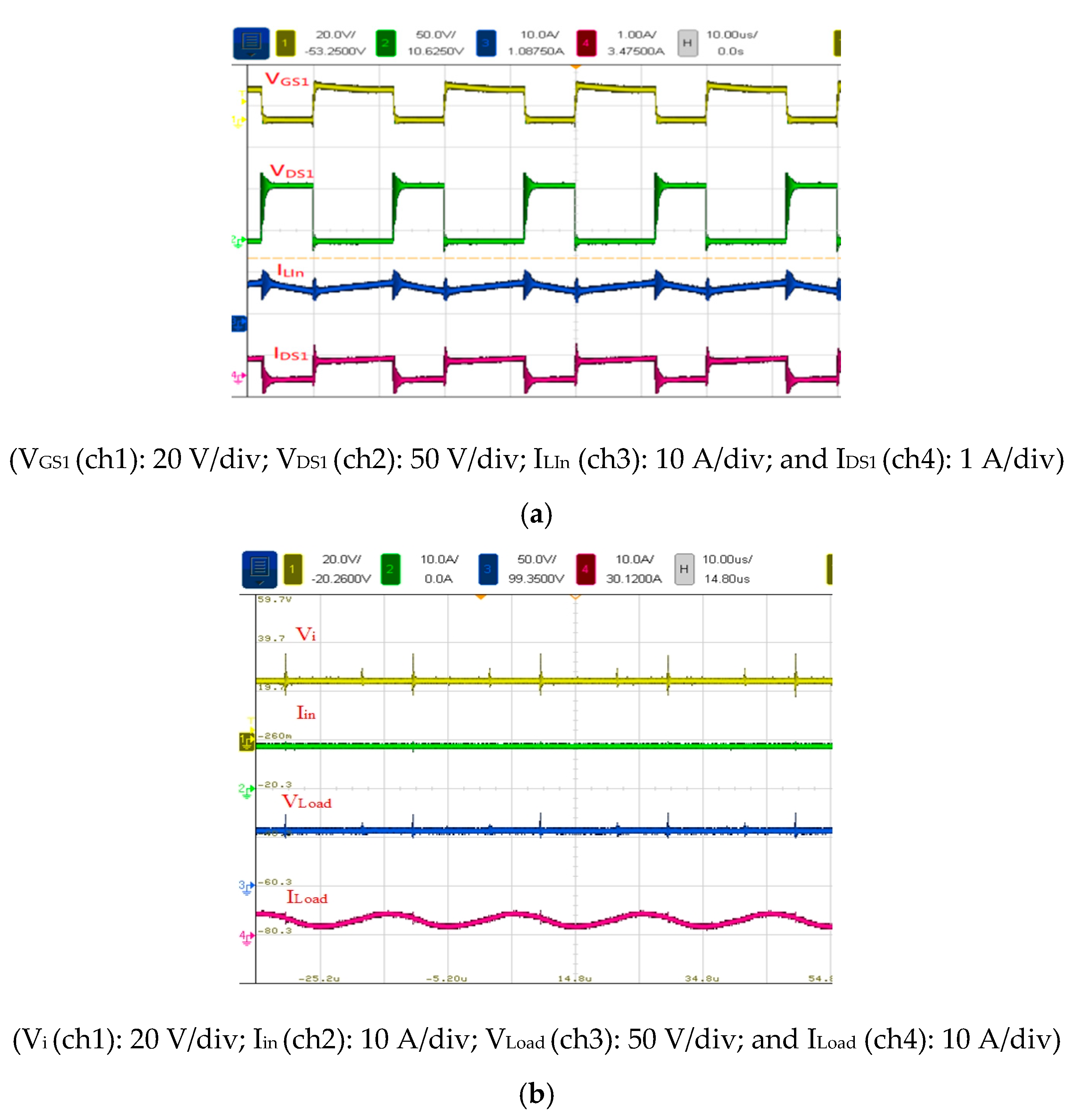
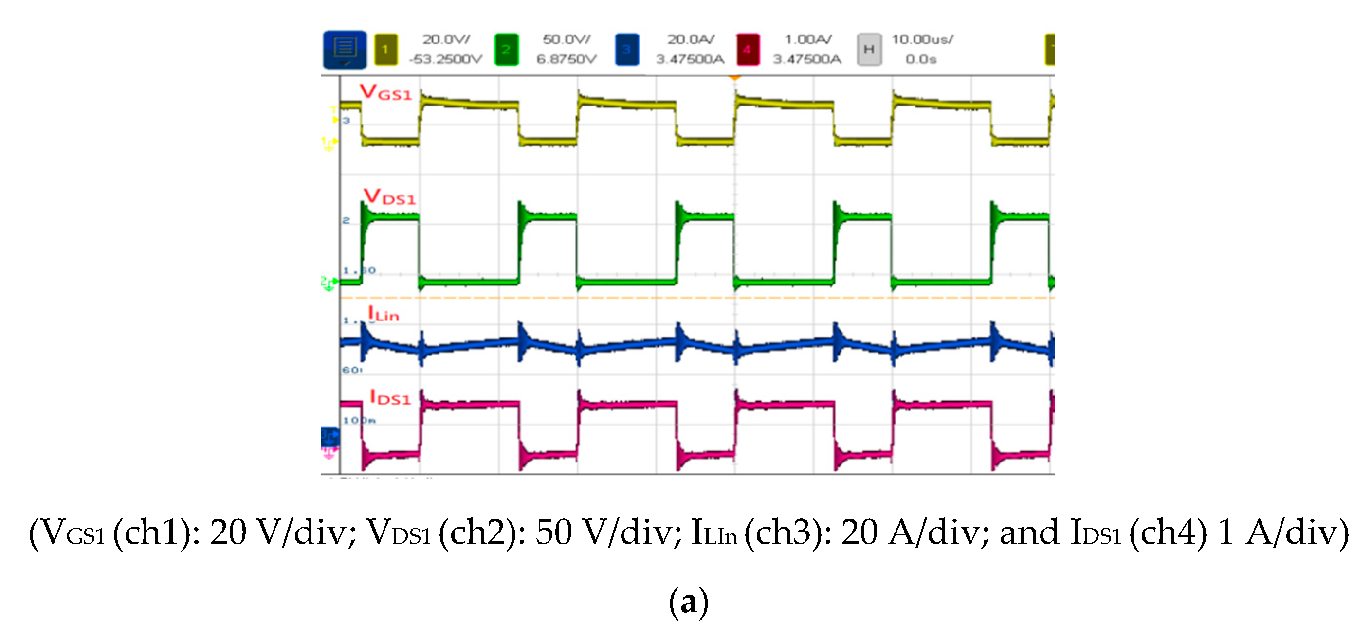
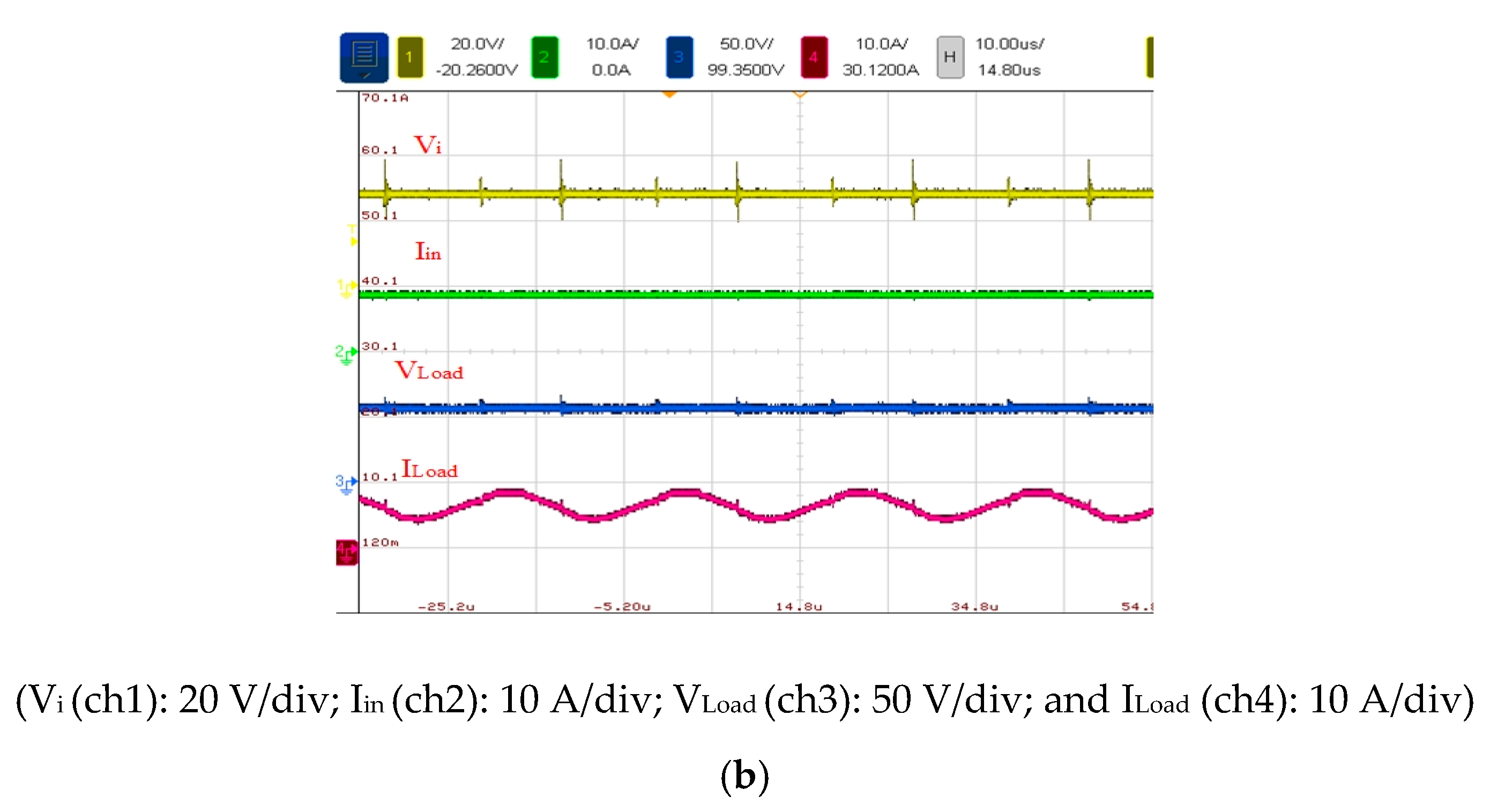
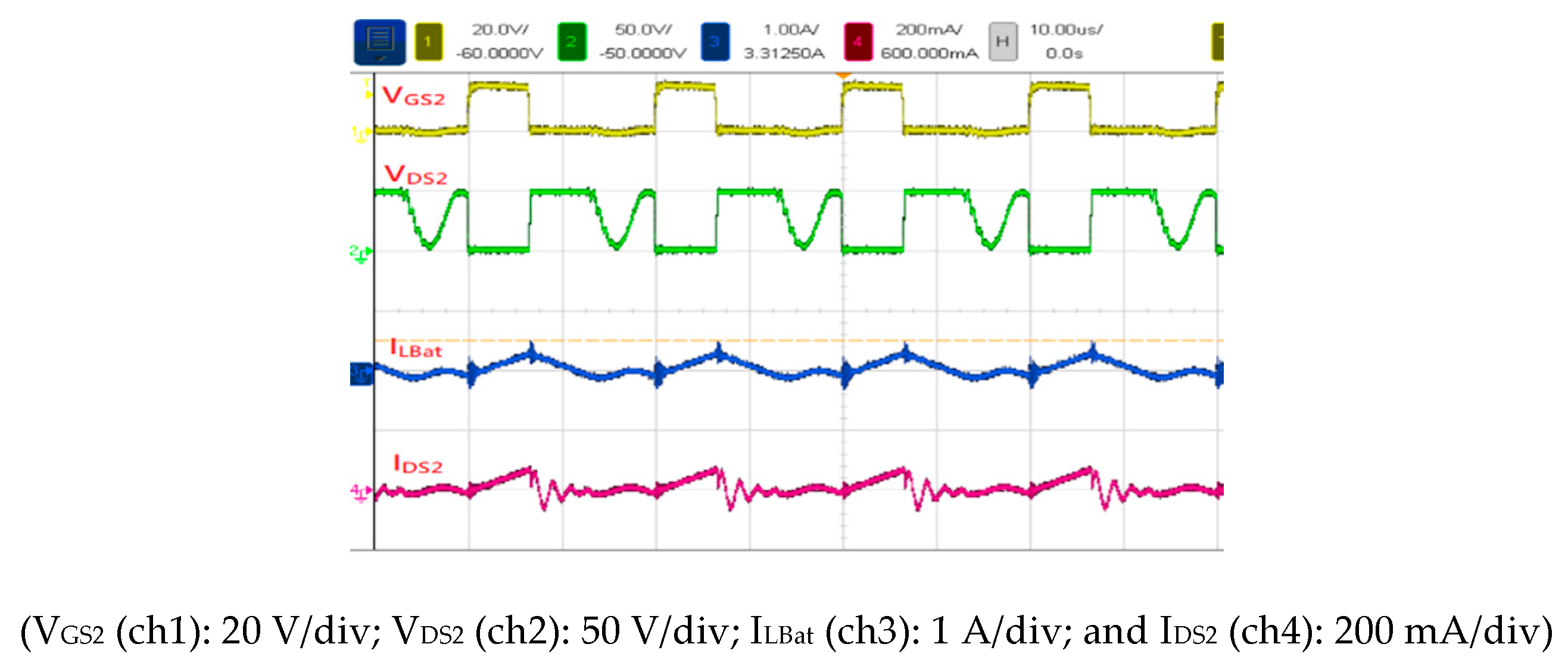
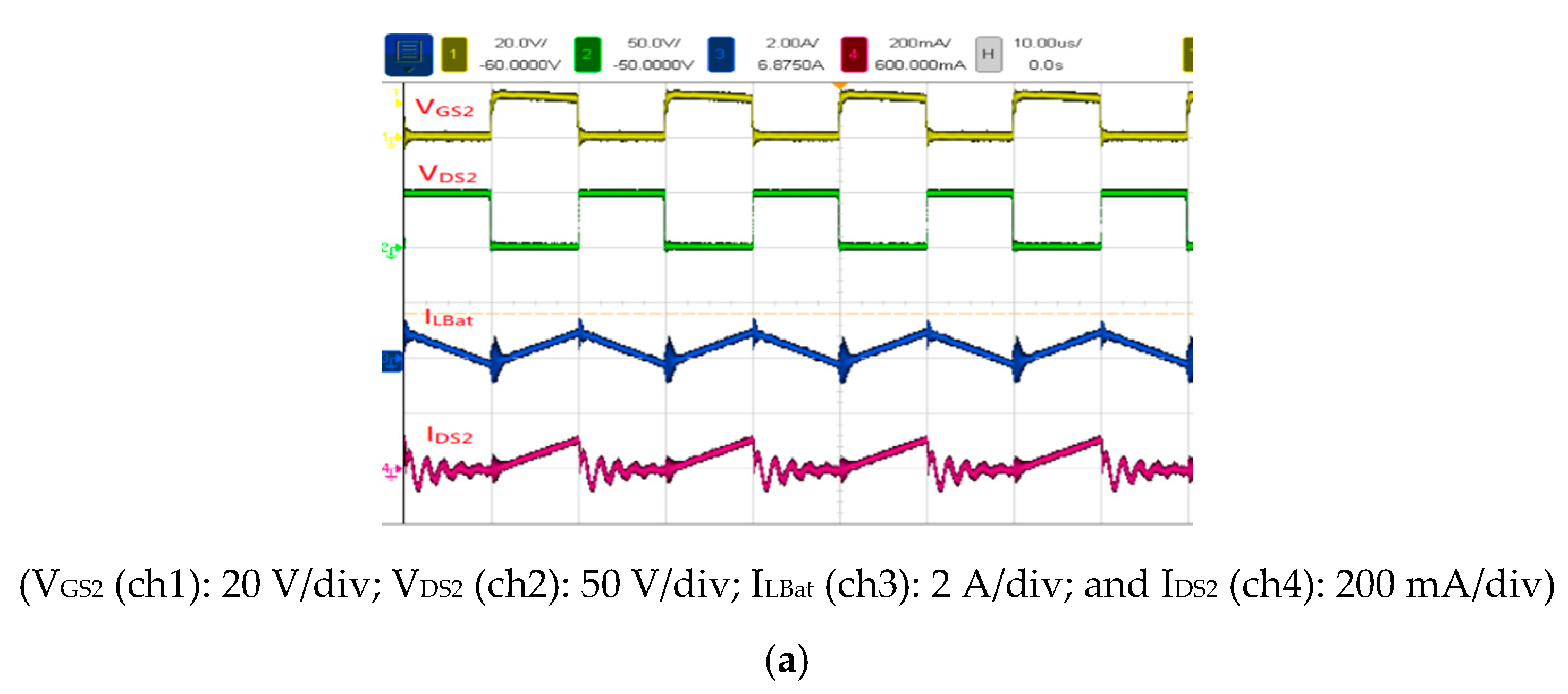
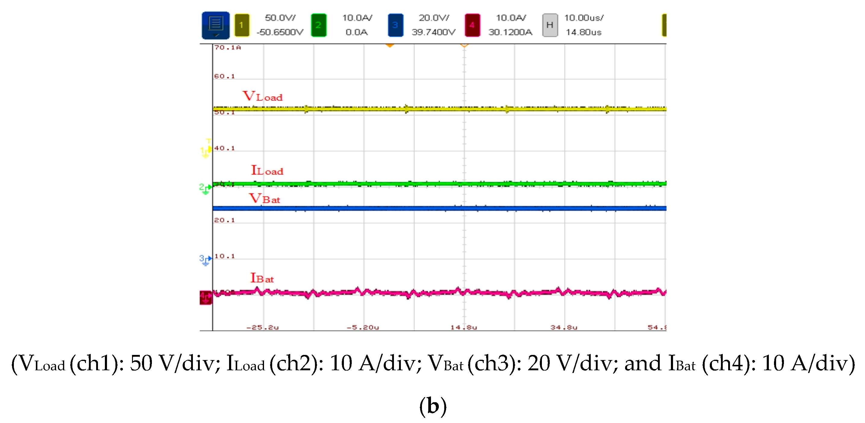
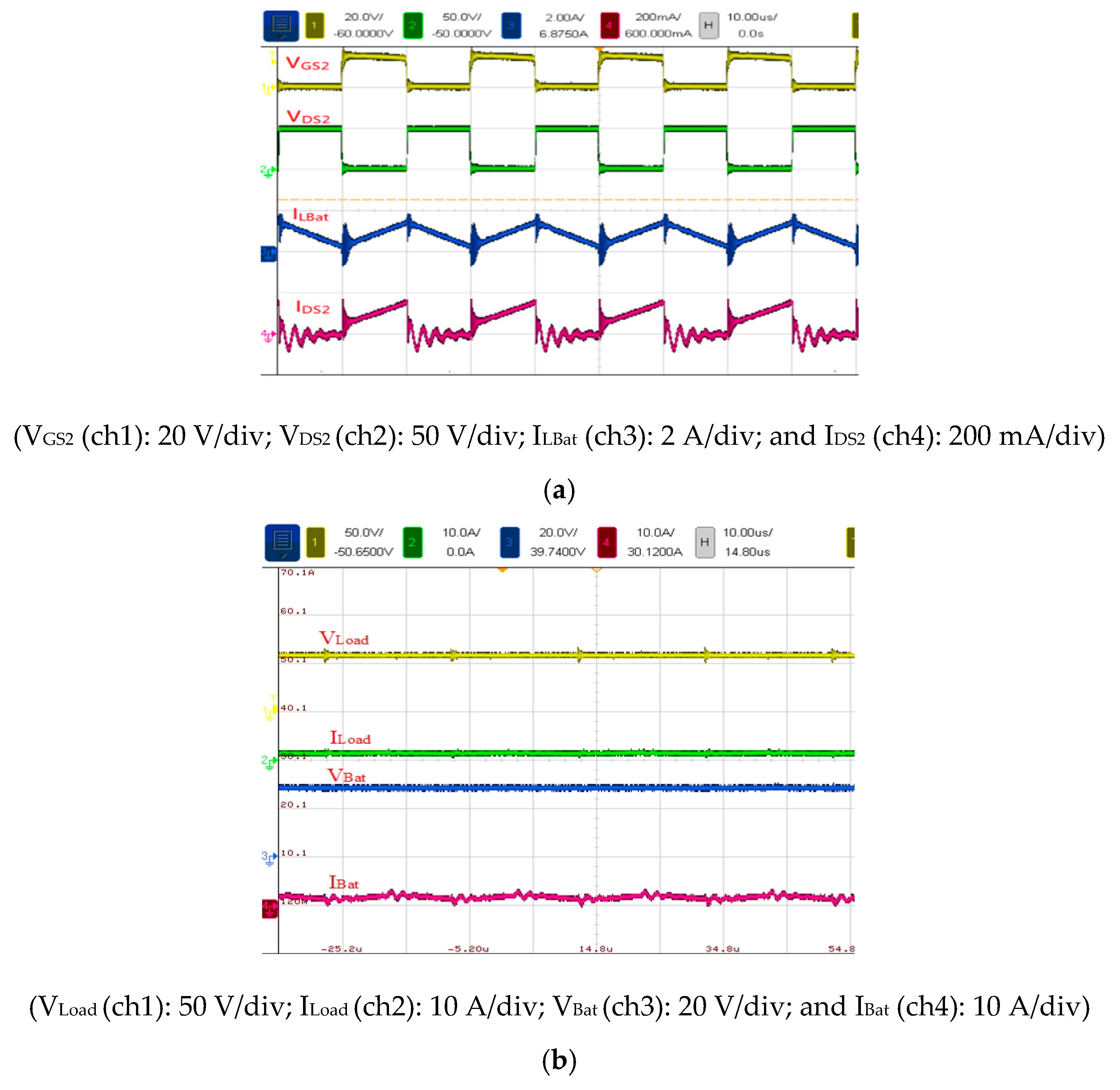
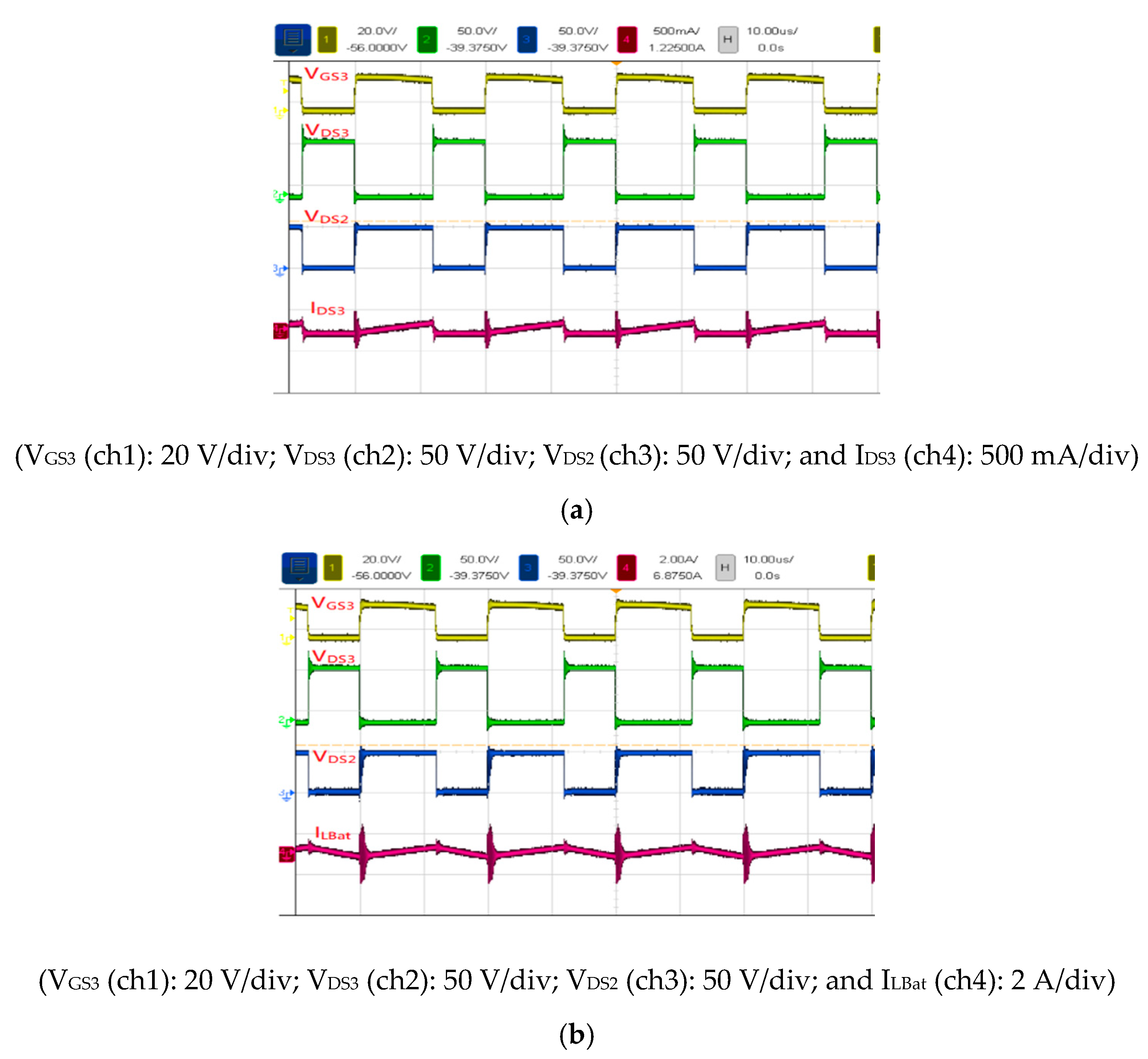
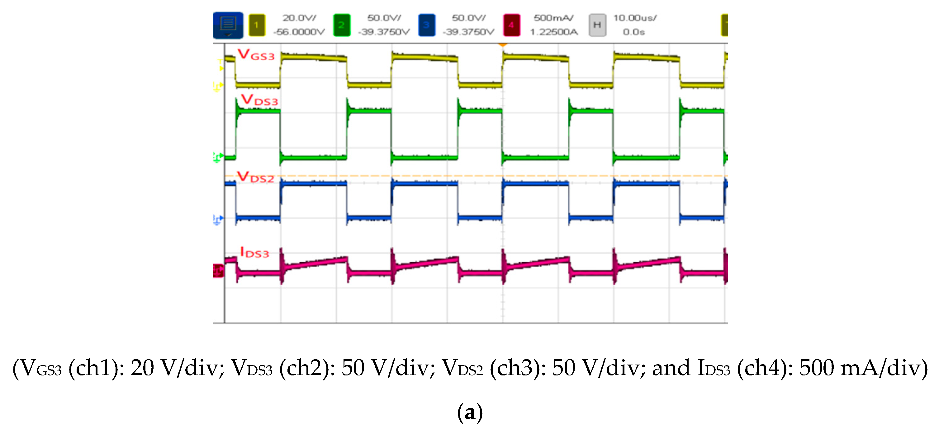
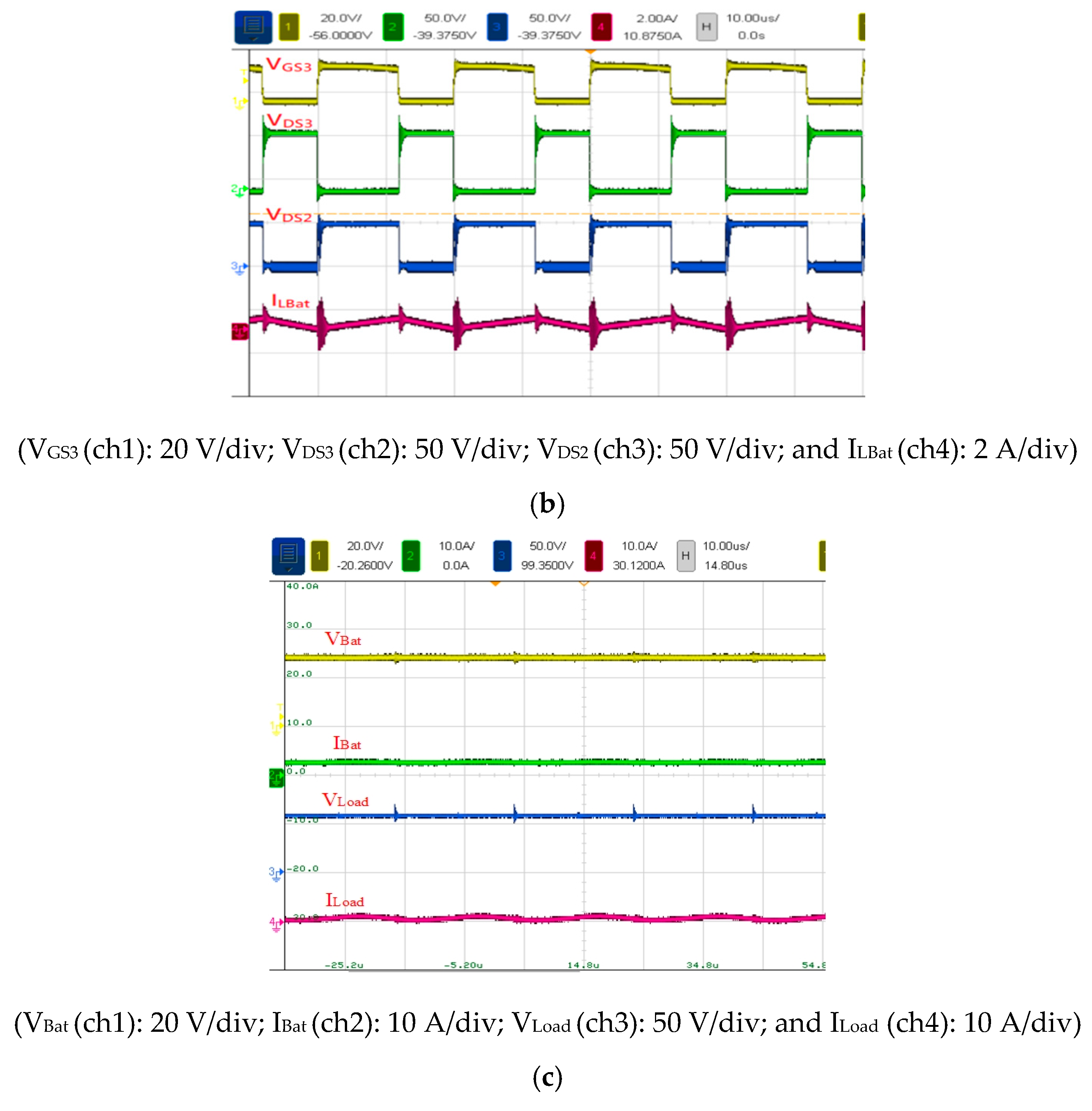
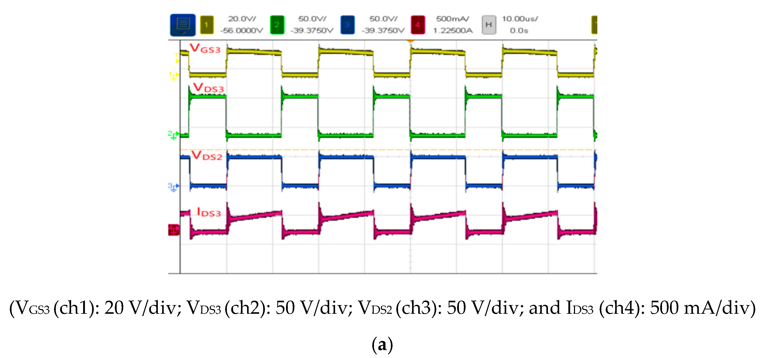
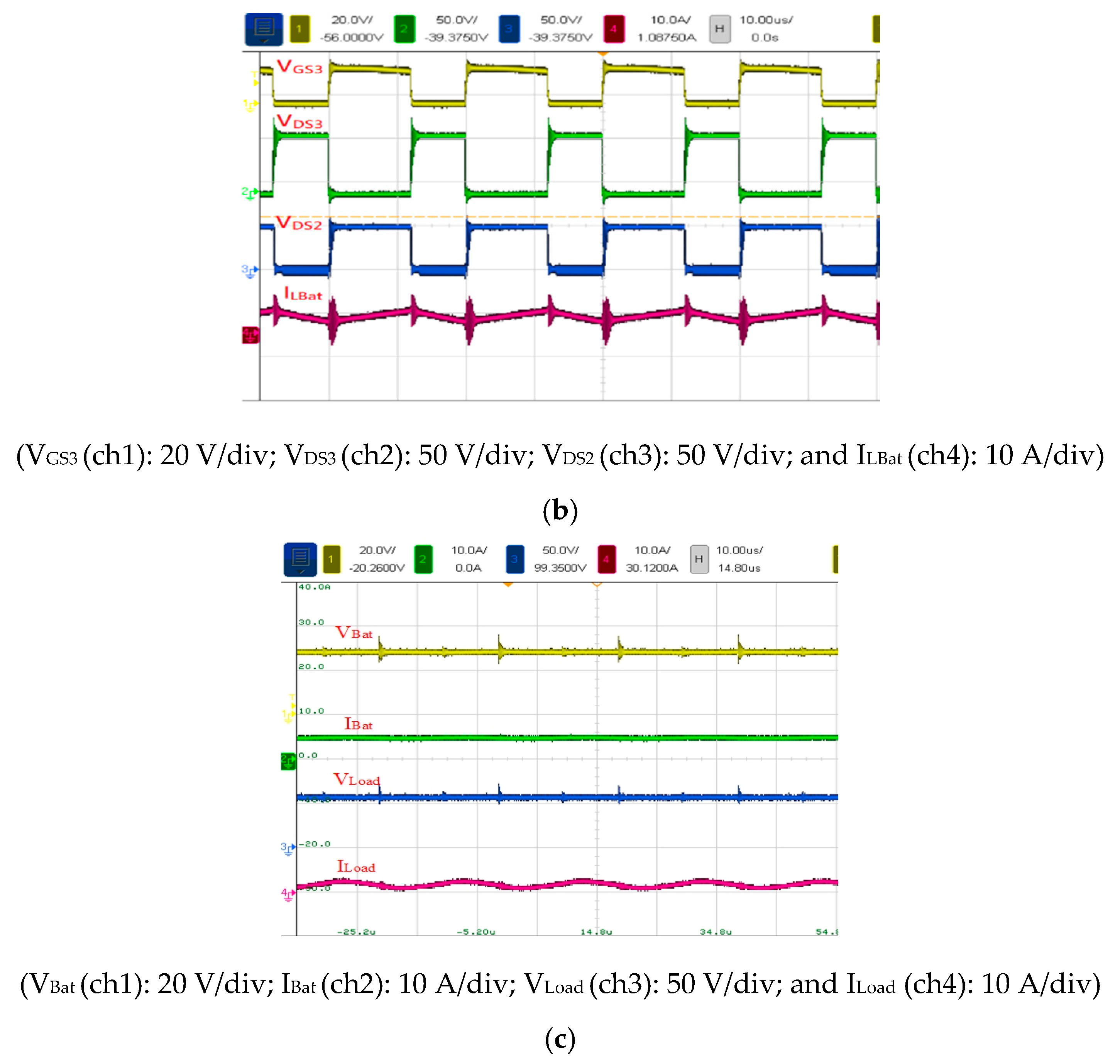
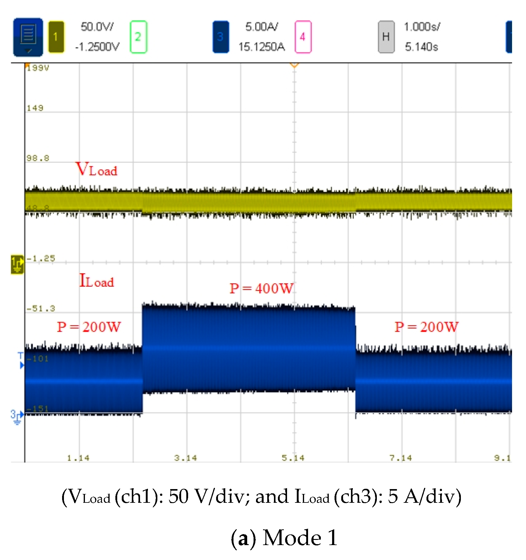
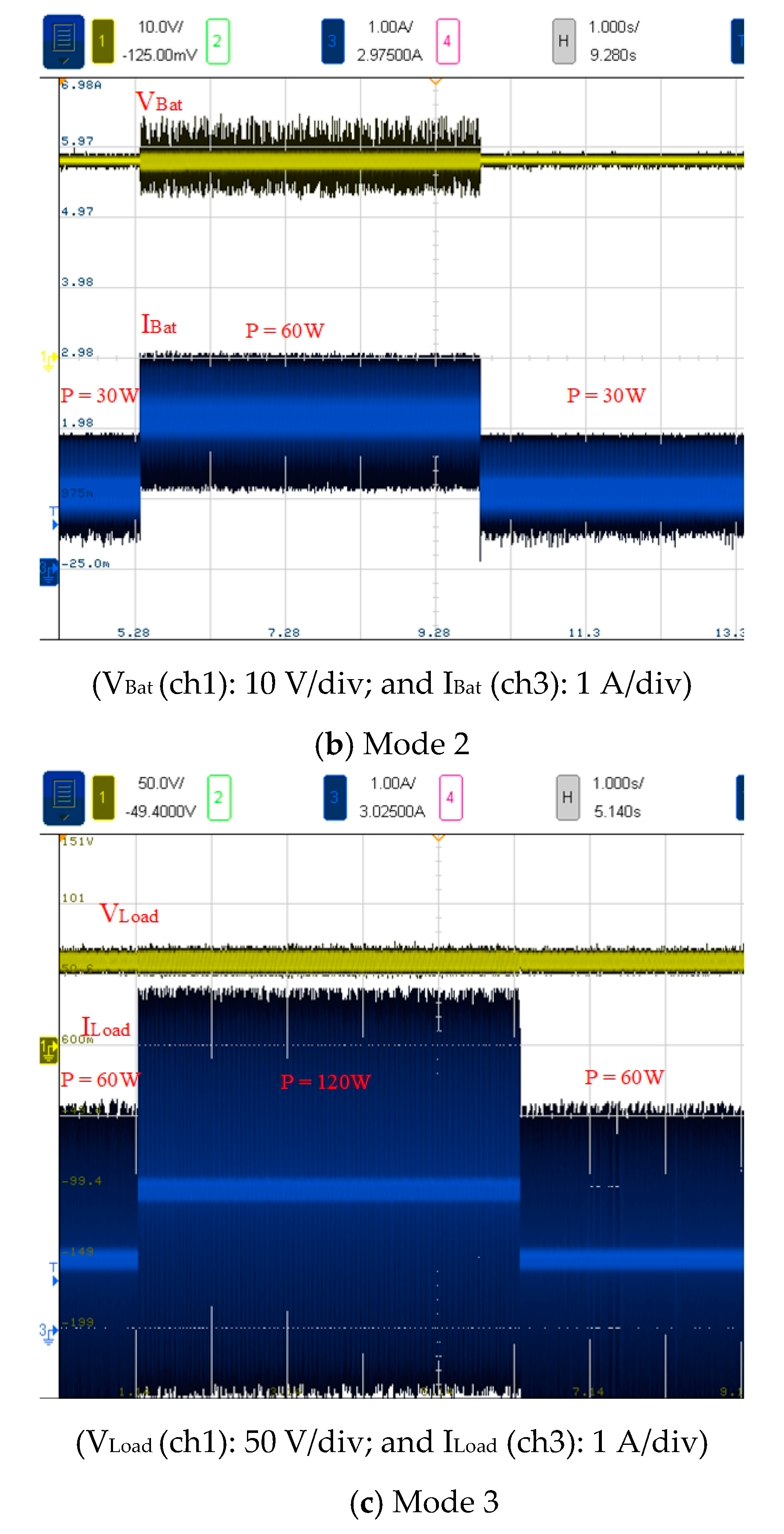
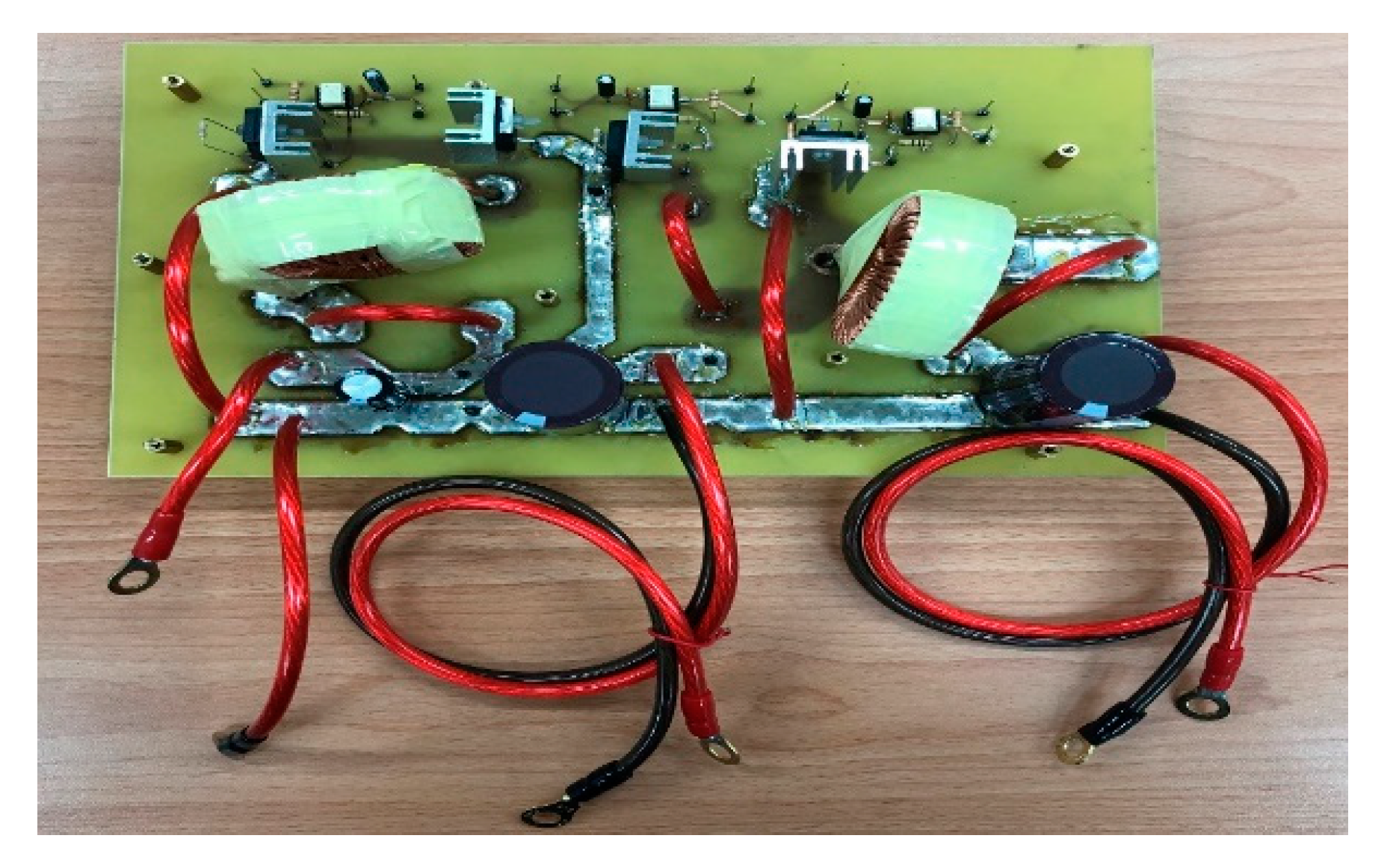
5. Experimental Results and Analysis
6. Conclusions
Author Contributions
Funding
Conflicts of Interest
References
- Taiwan’s Response to the Climate Change Framework Convention Information Network. Available online: http://www.tri.org.tw/unfccc/ (accessed on 10 September 2019).
- Ministry of Economic Affairs. Available online: https://www.re.org.tw/default.aspx (accessed on 12 September 2019).
- Boujelben, N.; Masmoudi, F.; Djemel, M.; Derbel, N. Design and comparison of quadratic boost and double cascade boost converters with boost converter. In Proceedings of the 2017 14th International Multi-Conference on Systems, Signals & Devices (SSD), Marrakech, Morocco, 28–31 March 2017; pp. 245–252. [Google Scholar]
- Ismail, E.H.; Al-Saffar, M.A.; Sabzali, A.J. High Conversion Ratio DC–DC Converters with Reduced Switch Stress. IEEE Trans. Circuits Syst. I Regul. Studys 2008, 55, 2139–2151. [Google Scholar] [CrossRef]
- Pressman, A.I.; Billings, K.; Morey, T. Switching Power Supply Design, 3rd ed.; Quanhua Book Company: Taipei, Taiwan, 2012. [Google Scholar]
- Zhao, Q.; Lee, F.C. High performance coupled-inductor DC-DC converters. In Proceedings of the Eighteenth Annual IEEE Applied Power Electronics Conference and Exposition, 2003. APEC ’03, Miami Beach, FL, USA, 9–13 February 2003; pp. 109–113. [Google Scholar]
- Huber, L.; Jovanovic, M.M. A design approach for server power supplies for networking applications. In Proceedings of the APEC 2000 Fifteenth Annual IEEE Applied Power Electronics Conference and Exposition (Cat. No.00CH37058), New Orleans, LA, USA, 6–10 February 2000; pp. 1163–1169. [Google Scholar]
- Feng, X.; Liu, J.; Lee, F.C. Impedance specifications for stable DC distributed power systems. IEEE Trans. Power Electron. 2002, 17, 157–162. [Google Scholar] [CrossRef]
- Wu, T.F.; Yu, T.-H. Unified approach to developing single-stage power converters. IEEE Trans. Aerosp. Electron. Syst. 1998, 34, 211–223. [Google Scholar]
- Luo, F.L.; Ye, H. Positive output super-lift converters. IEEE Trans. Power Electron. 2003, 18, 105–113. [Google Scholar]
- Zhao, Q.; Tao, F.; Lee, F.C. A front-end DC/DC converter for network server applications. In Proceedings of the 2001 IEEE 32nd Annual Power Electronics Specialists Conference (IEEE Cat. No.01CH37230), Vancouver, BC, Canada, 17–21 June 2001; pp. 1535–1539. [Google Scholar]
- Chen, F.; Amirahmadi, A.; Batarseh, I. Zero voltage switching Forward-Flyback Converter with efficient active LC snubber circuit. In Proceedings of the 2014 IEEE Applied Power Electronics Conference and Exposition—APEC 2014, Fort Worth, TX, USA, 16–20 March 2014; pp. 2041–2047. [Google Scholar]
- EPARC. Power Electronics Review, 2nd ed.; Quanhua Book Company: Taipei, Taiwan, 2013. [Google Scholar]
- Hart, D.W. Power Electronics; Quanhua Book Company: Taipei, Taiwan, 2013. [Google Scholar]
- Jianhua, W.; Fanghua, Z.; Chunying, G.; Ran, C. Modeling and analysis of a buck/boost bidirectional converter with developed PWM switch model. In Proceedings of the 8th International Conference on Power Electronics—ECCE Asia, Jeju, Korea, 30 May–3 June 2011; pp. 705–711. [Google Scholar]
- Mohammadi, M.R.; Farzanehfard, H. A new bidirectional ZVS-PWM Cuk converter with active clamp. In Proceedings of the 2011 19th Iranian Conference on Electrical Engineering, Tehran, Iran, 17–19 May 2011; pp. 1–6. [Google Scholar]
- Dimna Denny, C.; Shahin, M. Analysis of bidirectional SEPIC/Zeta converter with coupled inductor. In Proceedings of the 2015 International Conference on Technological Advancements in Power and Energy (TAP Energy), Kollam, India, 24–26 June 2015; pp. 103–108. [Google Scholar]
- Song, Y.; Enjeti, P.N. A new soft switching technique for bi-directional power flow, full-bridge DC-DC converter. In Proceedings of the Conference Record of the 2002 IEEE Industry Applications Conference. 37th IAS Annual Meeting (Cat. No.02CH37344), Pittsburgh, PA, USA, 13–18 October 2002; pp. 2314–2319. [Google Scholar]
- Ma, Z.; Hu, R. Zero-voltage-switching condition of isolated-type symmetrical half-bridge bidirectional DC/DC converter. In Proceedings of the 2011 International Conference on Electrical and Control Engineering, Yichang, China, 16–18 September 2011; pp. 2347–2350. [Google Scholar]
- Duan, R.; Lee, J. High-efficiency bidirectional DC-DC converter with coupled inductor. IET Power Electron. 2012, 5, 115–123. [Google Scholar] [CrossRef]
- Wai, R.; Liaw, J. High-Efficiency-Isolated Single-Input Multiple-Output Bidirectional Converter. IEEE Trans. Power Electron. 2015, 30, 4914–4930. [Google Scholar] [CrossRef]
- Zhang, B.; Wang, P.; Bei, T.; Li, X.; Che, Y.; Wang, G. Novel topology and control of a non-isolated three port DC-DC converter for PV-battery power system. In Proceedings of the 2017 20th International Conference on Electrical Machines and Systems (ICEMS), Sydney, Australia, 11–14 August 2017; pp. 1–6. [Google Scholar]
- Li, W.; Xu, C.; Luo, H.; Hu, Y.; He, X.; Xia, C. Decoupling-Controlled Triport Composited DC/DC Converter for Multiple Energy Interface. IEEE Trans. Ind. Electron. 2015, 62, 4504–4513. [Google Scholar] [CrossRef]
- Hu, Y.; Xiao, W.; Cao, W.; Ji, B.; Morrow, D.J. Three-Port DC–DC Converter for Stand-Alone Photovoltaic Systems. IEEE Trans. Power Electron. 2015, 30, 3068–3076. [Google Scholar] [CrossRef]
- Das, P.; Mousavi, S.A.; Moschopoulos, G. Analysis and Design of a Nonisolated Bidirectional ZVS-PWM DC–DC Converter with Coupled Inductors. IEEE Trans. Power Electron. 2010, 25, 2630–2641. [Google Scholar] [CrossRef]
- Do, H. Nonisolated Bidirectional Zero-Voltage-Switching DC–DC Converter. IEEE Trans. Power Electron. 2011, 26, 2563–2569. [Google Scholar] [CrossRef]
- Liang, T.; Lee, J. Novel High-Conversion-Ratio High-Efficiency Isolated Bidirectional DC–DC Converte. IEEE Trans. Ind. Electron. 2015, 62, 4492–4503. [Google Scholar] [CrossRef]
- Cheng, T.; Lu, D.D.; Qin, L. Non-Isolated Single-Inductor DC/DC Converter with Fully Reconfigurable Structure for Renewable Energy Applications. IEEE Trans. Circuits Syst. Ii Express Briefs 2018, 65, 351–355. [Google Scholar] [CrossRef]
- Zeng, J.; Qiao, W.; Qu, L. An Isolated Three-Port Bidirectional DC–DC Converter for Photovoltaic Systems with Energy Storage. IEEE Trans. Ind. Appl. 2015, 51, 3493–3503. [Google Scholar] [CrossRef]
- Uno, M.; Oyama, R.; Sugiyama, K. Partially Isolated Single-Magnetic Multiport Converter Based on Integration of Series-Resonant Converter and Bidirectional PWM Converter. IEEE Trans. Power Electron. 2018, 33, 9575–9587. [Google Scholar] [CrossRef]
- Wu, Y.-E.; Chiu, P.-N. A High-Efficiency Isolated-Type Three-Port Bidirectional DC/DC Converter for Photovoltaic Systems. Energies 2017, 10, 434. [Google Scholar] [CrossRef]


| Parameter | Specification | |
| Input PV voltage Vin | 24 V | |
| Battery voltage VBat | 24 V | |
| Load bus voltage VLoad | 48 V | |
| Maximus output battery power | 60 W | |
| Maximus output load bus power | 400 W | |
| Switching frequency fs | 50 kHz | |
| Component | Model | Specification |
| S1, S2, S3 | IRFP4332 | 250 V/57 A |
| D1 | MBR40200 | 200 V/40 A |
| CIn | Electrolytic Capacitor | 100 μF/100 V |
| CLoad, CBat | Electrolytic Capacitor | 470 μF/450 V |
| LIn, LBat | MPP Ring Core | 100 μH |
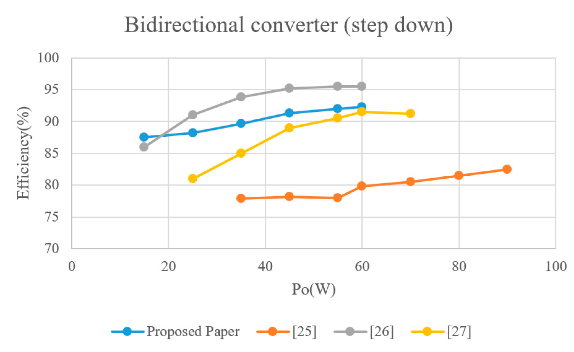
| References | Proposed Converter | Reference [25] | Reference [26] | Reference [27] |
|---|---|---|---|---|
| Topology | Non-Isolated | Non-Isolated | Non-Isolated | Non-Isolated |
| Input Voltage | 24 V | 24–30 V | 48 V | 24 V |
| Output Voltage | 58 V | 200 V | 120 V | 200 V |
| Output Power | 120 W | 200 W | 100 W | 200 W |
| Number of Switches | 3 | 3 | 2 | 4 |
| Number of Diodes | 1 | 0 | 0 | 0 |
| Number of Inductors | 2 | 2 | 1 | 2 |
| Number of Capacitors | 3 | 1 | 2 | 3 |
| Number of Coupled-inductors | 0 | 1 | 1 | 1 |
| Output Terminal | 2 | 2 | 2 | 2 |
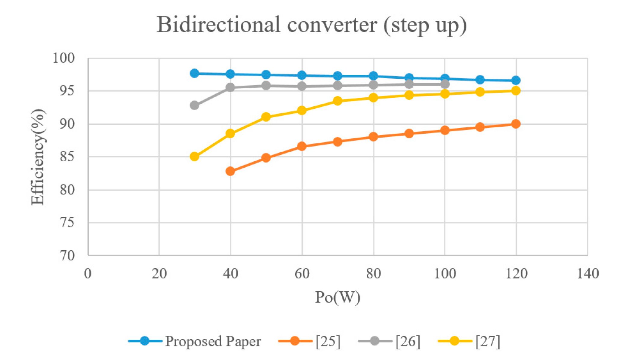
| Maximum Conversion Efficiency (Step up/Step down) | 96.6%/92% | 91.5%/91% | 95.6%/95.3% | 96%/95% |
| Cost | Low | High | Medium | High |
| Converter Operational Mode | 2 | 2 | 2 | 2 |
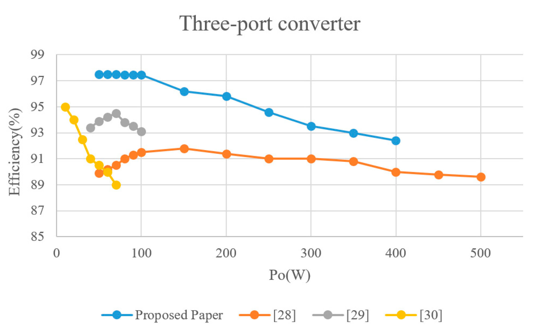
| References | Proposed Converter | Reference [28] | Reference [29] | Reference [30] |
|---|---|---|---|---|
| Topology | Non-Isolated | Non-Isolated | Isolated | Isolated |
| Input Voltage | 24 V | 17 V | 16 V | 36 V |
| Battery Voltage | 28 V | 36 V | 7.5 V | 16 V |
| Load Bus Voltage | 58 V | 24 V | 50 V | 45 V |
| Output Power | 400 W | 500 W | 120 W | 150 W |
| Number of Switch | 3 | 4 | 3 | 2 |
| Number of Diode | 1 | 5 | 4 | 4 |
| Number of Transformer | 0 | 0 | 1 | 1 |
| Number of Inductor | 2 | 1 | 2 | 0 |
| Number of Capacitor | 3 | 3 | 5 | 4 |
| Transformer Turns | 0 | 0 | 5:14 | 9:25 |
| Output Terminal | 2 | 2 | 2 | 2 |
| Maximum Conversion Efficiency (Step-up) | 96.6% | 85% | 94.5% | 87.4% |
| Converter Mode | 3 | 7 | 3 | 3 |
Publisher’s Note: MDPI stays neutral with regard to jurisdictional claims in published maps and institutional affiliations. |
© 2020 by the authors. Licensee MDPI, Basel, Switzerland. This article is an open access article distributed under the terms and conditions of the Creative Commons Attribution (CC BY) license (http://creativecommons.org/licenses/by/4.0/).
Share and Cite
Wu, Y.-E.; Lin, X.-Y. A Novel Non-Isolated Three-Port Bidirectional DC/DC Converter for Photovoltaic Electric Scooter Charging Stations. Electronics 2020, 9, 1741. https://doi.org/10.3390/electronics9101741
Wu Y-E, Lin X-Y. A Novel Non-Isolated Three-Port Bidirectional DC/DC Converter for Photovoltaic Electric Scooter Charging Stations. Electronics. 2020; 9(10):1741. https://doi.org/10.3390/electronics9101741
Chicago/Turabian StyleWu, Yu-En, and Xiu-Yi Lin. 2020. "A Novel Non-Isolated Three-Port Bidirectional DC/DC Converter for Photovoltaic Electric Scooter Charging Stations" Electronics 9, no. 10: 1741. https://doi.org/10.3390/electronics9101741
APA StyleWu, Y.-E., & Lin, X.-Y. (2020). A Novel Non-Isolated Three-Port Bidirectional DC/DC Converter for Photovoltaic Electric Scooter Charging Stations. Electronics, 9(10), 1741. https://doi.org/10.3390/electronics9101741