Article

An Ultra-Low Quiescent Current Under-Voltage Lockout Circuit for a High-Voltage Gate Driver IC

1
School of Electronics Engineering, Kyungpook National University, Daegu 41566, Korea
2
School of Electronic and Electrical Engineering, Kyungpook National University, Daegu 41566, Korea
Electronics 2020, 9(10), 1729; https://doi.org/10.3390/electronics9101729
Submission received: 28 September 2020 / Revised: 17 October 2020 / Accepted: 19 October 2020 / Published: 20 October 2020
(This article belongs to the Section Power Electronics)

Abstract

:
An ultra-low quiescent current under-voltage lockout (UVLO) circuit for a high-voltage gate driver integrated circuit (HVIC) is described for application in portable devices. The UVLO circuit consumes the static current in the high-side circuitry and the resistive divider used to detect the supply-voltage was the major consumer of power in the circuit. Hence, a supply-voltage sensor based on a diode-connected metal–oxide–semiconductor field-effect transistor (MOSFET) with a voltage limiter design is proposed to ensure low power consumption. Unlike the conventional UVLO design, where a resistive divider is used, the proposed structure dissipates the negligible current at a low supply-voltage and significantly reduces the static current at the nominal and high supply-voltage. The high-side quiescent current using the proposed design and the conventional designs at various supply-voltage levels are analyzed. In the proposed structure, the size of the voltage sensor is considerably smaller when compared with those in conventional designs.

1. Introduction

The high-voltage gate driver integrated circuits (HVICs) are gaining popularity because of the fast-growing demand for portable home appliances and tablet computers. Portable devices are powered by batteries. The boost converter generates a high-voltage signal from these batteries such as signals with voltages of 50–200 V (Figure 1). An HVIC is used to switch high-voltage signals and drive the coil or specific load conditions [1,2,3,4]. In such applications, the driver spends majority of the time in the sleep mode and wakes up occasionally for switching operations. The average power consumption of the HVICs is determined based on the sleep mode operation, which should consume very low power to achieve long battery lifetimes.
The HVIC consists of high-side circuitry, low-side circuitry, and a high-voltage level shifter (Figure 2a). To reduce the power consumption of the HVICs, a shut-down (SD) pin is added to indicate the sleep mode of an HVIC. Although the SD signal can reduce the power consumption of the low-side circuitry and high-voltage level shifter [4,5,6,7], the power consumption of the high-side circuitry cannot be decreased because the high-side region is isolated from the low-side region. Furthermore, an additional high-voltage level shifter is required to send the SD signal to the high-side region, which is undesirable from the cost perspective.
The under-voltage lockout (UVLO) protection is an essential part of the HVIC to disable the driver at low supply-voltage and protect the device from damage [8,9,10,11]. The UVLO circuits are required for the low-side and high-side region separately since the supply-voltages of both sides are isolated from each other. Although a low-side UVLO can be fully turned off by the SD signal, a high-side UVLO still consumes the quiescent current which is a majority of the quiescent current in the high-side region [10,11]. Therefore, minimizing the power consumption of the UVLO in the high-side region is an important approach to improve the battery lifetime. Figure 2b shows the conventional UVLO structure. The power-on-reset (POR) circuit can be reconfigured as a coarse UVLO to reduce the power consumption of the UVLO [10]. The supply-voltage sensor is disconnected from the supply-voltage when the output of the POR circuit is high. Thus, the static current at a low supply-voltage can be eliminated while dissipating the same current at a nominal supply-voltage. The power consumption of the UVLO can also be reduced using a slope-based POR circuit [11]. Although the current consumption can be reduced by removing the static current in the POR circuit, only a minor improvement can be observed because the POR circuit is not a major factor associated with the UVLO power consumption.
In this paper, a low quiescent current UVLO circuit is described that can reduce the power consumption of the HVIC in the sleep mode and enhance the battery lifetime. The proposed supply-voltage sensor dissipates the negligible current at a low supply-voltage and significantly reduces the static current at the nominal and high supply-voltage. In addition, the size of the UVLO can be considerably reduced by preventing the resistive divider from detecting the supply-voltage level.
This paper is organized as follows. Section 2 describes the architecture of HVIC. Section 3 introduces the proposed low-quiescent current UVLO structure. Section 4 describes the simulation results and the conclusion follows in Section 5.

2. High-Voltage Gate Driver IC

2.1. Architecture

Figure 2a shows the full block diagram of a half-bridge type HVIC comprising a high-side and low-side gate driver. The input signal is received through the Schmitt trigger block, and the dead-time generator generates input signals for both high-side and low-side drivers with the dead-time to prevent shoot-through current between VB and COM in the output stage [4,12]. A short-pulse generator is used to drive the high-voltage laterally diffused MOSFET (LDMOS) in the high-voltage level shifter to reduce the power consumption at the level shifter. The short-pulse generator generates the SET and RESET short pulses synchronized at the rising and falling edges of the INHS signal, respectively. The input signal can be restored from these short pulses using the SR latch in the high-side region [13,14,15,16,17,18,19]. However, the parasitic capacitance of the LDMOS and dV/dt arises from VB rising, which will introduce common-mode noise in the level shifter. This noise may lead the incorrect pulses into the SR latch. Therefore, a noise canceller can be employed to remove the common-mode noise during transitions [14]. In addition, the low-side and high-side circuitries contain UVLO protection circuits to perform the switching operation at a sufficiently high supply-voltage.

2.2. Under-Voltage Lockout Circuit

In case of the high-side circuitry, the static current only flows through the high-side UVLO protection circuit. Figure 2b describes the circuit diagram of the conventional high-side UVLO [10,11]. The reference current independent of the supply-voltage (VBS) is generated by the current bias circuit, and the POR circuit generates the reset pulse to prevent any latch-on state during power-up. The comparator compares the VBS level with the reference voltage to ensure that the VBS level is greater than the minimum operating voltage. The VBS level is detected using the resistive divider and the Zener diode generates the reference voltage. The hysteresis can be added by controlling the ratio of the resistive divider. When the supply-voltage is rising, R1 and R2 sense the supply-voltage, while R3 is added if the supply-voltage is falling. Hence, the positive and negative UVLO levels can be determined as follows:
V U V L O + = V R E F R 1 + R 2 R 2
V U V L O = V R E F R 1 + R 2 + R 3 R 2 + R 3
where VREF is the reference voltage generated by the Zener diode.
In the conventional UVLO circuit, the resistive divider always draws the static current, which is proportional to the supply-voltage. Furthermore, it is the dominant quiescent current source, especially at a high supply-voltage. The current can be reduced by increasing the size of the resistor. However, this requires a large area and increases the cost.

3. Low-Quiescent Current High-Side UVLO

An active resistor using the diode-connected MOSFET (MOS-diode) can be employed for implementing a supply-voltage sensor to reduce the current at the resistive divider (Figure 3a). The resistance of the MOS-diode can be represented as follows:
R d i o d e = 1 g m = 1 2 k L W I D
where k′ is the process transconductance parameter. The resistance of the MOS-diode is controlled by adjusting the aspect ratio (W/L). Because the resistance of the smaller-sized MOS-diode is considerably greater than that of the general-purpose poly or diffusion resistor, exploiting the MOS-diode can reduce both the current consumption and size associated with the supply-voltage sensor.
Figure 3b shows the supply-voltage sensor based on the MOS-diode. By assuming that same sized MOSFETs are used to implement the MOS-diode, the supply-voltage (VBS) can be expressed as follows:
V B S = n V G S = n ( V T + V o v )
where n is the number of stacked MOS-diode, and VT and VOV are the threshold and overdrive voltage of the MOSFET, respectively. Therefore, the current at the MOS-diode divider can be expressed as follows:
I D = k W 2 L ( V B S n V T ) 2
Unlike the typical resistive divider, the current consumption of the MOS-diode divider is proportional to the square of supply-voltage. Hence, the static current can be significantly reduced at a low supply-voltage. However, this can also result in considerably high current consumption at a high supply-voltage.
To reduce the current of the supply-voltage sensor at a high supply-voltage, a MOS-diode divider with a voltage limiter is proposed (Figure 3c). The voltage limiter is implemented by introducing an additional NMOS transistor (MN) observed under one MOS-diode below the VSEN node, and the gate voltage is connected to VREF. When VSEN is less than VREF, MN is fully turned on which is at the triode region and the proposed structure works the same as the MOS-diode divider structure. The resistance of MN increases if the supply-voltage increases and VGS.MN decreases. Once VSEN becomes greater than VREFVSG.MP2 + VGS.MN, MN enters the saturation region and limits the source voltage of MN. VGS.MN should be higher than VSG.MP2 to ensure that MN can limit the voltage when VSEN becomes greater than VREF. Even though the supply-voltage is increasing, the source voltage of MN is maintained as VSENVGS.MN, and a constant current is dissipated by the supply-voltage sensor. Therefore, the proposed structure can not only reduce the current at a low supply-voltage but also prevent high current consumption at a high supply-voltage.
Figure 4 shows the proposed high-side UVLO circuit using the MOS-diode divider with a voltage limiter. The hysteresis comparator is employed to ensure the stable switching operation instead of controlling the number of MOS-diode devices in the supply-voltage sensor. Thus, the same static current can be maintained with respect to the supply-voltage sensor when VBS is increased to trigger VUVLO+ and VBS is decreased to trigger VUVLO−.

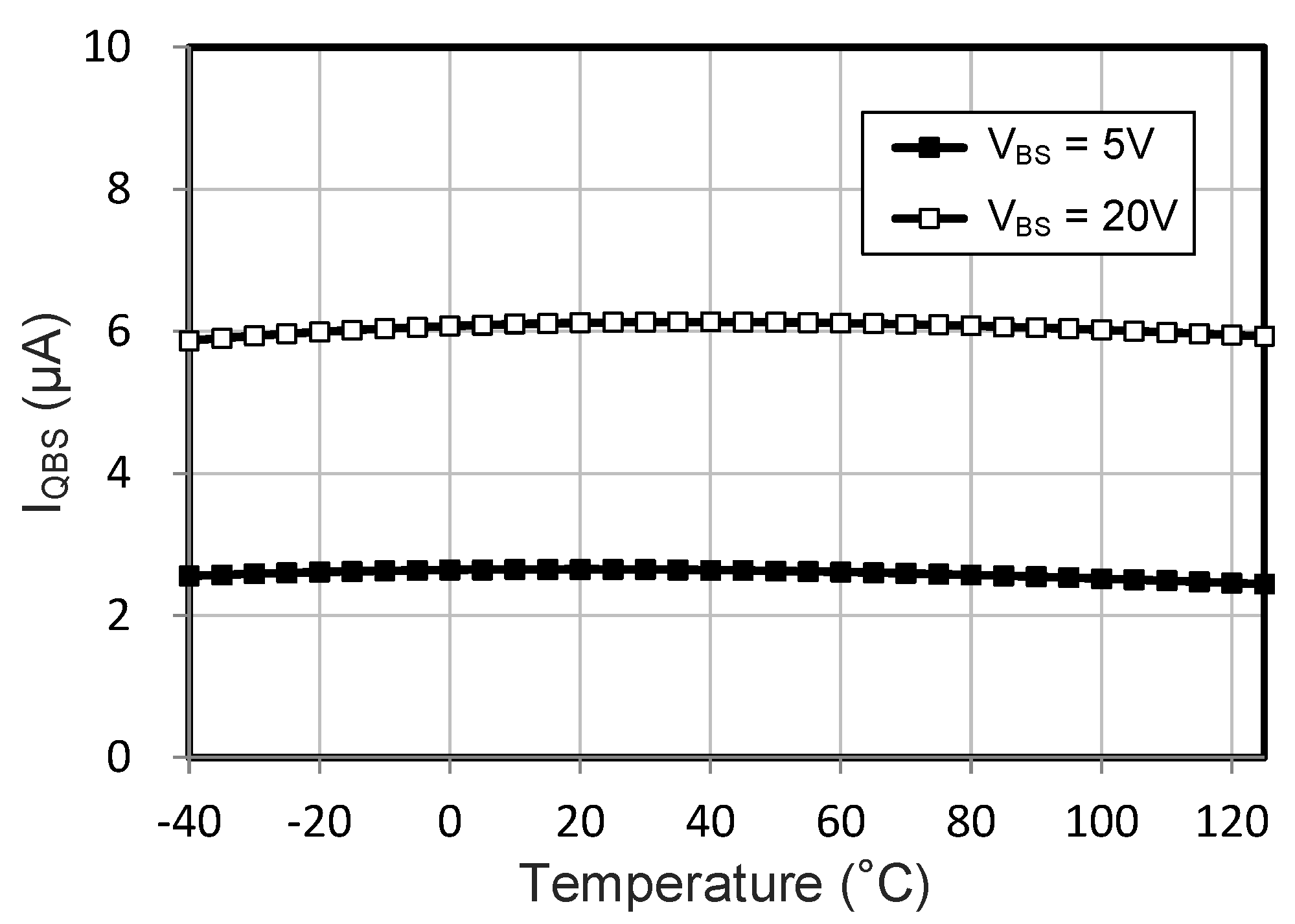
4. Simulation Results

A proposed UVLO is designed in 3.8 μm 25 V CMOS devices to provide the VBS level up to 25 V. Cadence Spectre tool is used for the simulation. Figure 5 shows the simulated current consumption of different types of voltage sensors in high-side UVLO. The total resistance of the resistive divider is set to 650 kΩ (R1 = 100 kΩ, R2 = 400 kΩ, and R3 = 150 kΩ), which is a practical value obtained by considering the tradeoff between the size and current consumption. A MOS-diode divider is designed to dissipate 1 µA at a supply-voltage of 8 V that is sufficiently fast to detect the supply-voltage through the MOS-diode structure. Although the current of the MOS-diode divider is considerably smaller than that of the resistive divider, especially at low and nominal supply-voltages, high current is consumed at a high supply-voltage because the current is proportional to the square of the supply-voltage. However, even at a high supply-voltage, the MOS-diode divider with a voltage limiter can maintain very low current consumption because the current is limited when VSEN is greater than VREFVSG.MP2 + VGS.MN.
The size of the resistive divider is 5136 µm2 (L = 44.9 µm, W = 4.4 µm, and mul = 26) for a given technology. The MOS-diode divider which uses 3.8 µm 25 V CMOS devices can be implemented with a size of 170 µm2 (L × W), which is 30 times smaller than the resistive divider.
Figure 6 shows the transient response of the proposed UVLO circuit at different temperatures. The VUVLO+/VUVLO− levels are 8.38/7.82, 8.64/8.08, and 9.03/8.43 V at −40, 25, and 125 °C, respectively. The temperature variation is mainly caused by the reference voltage level variation from the Zener diode.
Figure 7 and Figure 8 show the Monte-Carlo simulation results of the quiescent current consumption of the conventional high-side UVLO and proposed high-side UVLO, respectively. The conventional UVLO design consumes 13.1 and 37.3 µA at VBS of 5 and 20 V, while the proposed UVLO design consumes 2.6 and 6.1 µA at VBS of 5 and 20 V, respectively. The quiescent current can be reduced by 80.2% and 83.6% at VBS of 5 and 20 V, respectively, by employing the proposed design.
Figure 9 shows the quiescent current of the high-side UVLO circuits at different supply-voltage levels for different types of supply-voltage sensors. The quiescent current consumption can be significantly reduced at low as well as high supply-voltages because of the quiescent current of the supply-voltage sensor is significantly reduced over the entire supply-voltage range by employing the proposed design.
Figure 10 shows the quiescent current of the proposed structure by varying the temperature from −40 to 125 °C at VBS of 5 and 20 V. Although the quiescent current of the proposed supply-voltage sensor is increased when the temperature rises, the increased amount is sufficiently small compared to total quiescent current. Moreover, the temperature coefficient of the bias current is second order compensated by applying the appropriate temperature coefficient at RS in the current bias circuit (Figure 2b). The temperature coefficient of RS can be adjusted by combining diffusion resistors and poly resistors that have a positive temperature coefficient and a complementary temperature coefficient, respectively. Hence the quiescent current of the proposed structure shows an almost constant value over the temperature variation.
The quiescent current of the high-side circuitry without UVLO consumes approximately 1 nA [10], which is negligible when compared with that consumed by the circuitry with UVLO. Therefore, the quiescent current of high-side UVLO can be considered as the quiescent current of high-side circuitry. Table 1 summarizes the quiescent current of proposed structure and provides a comparison with prior works that contain the high-side UVLO circuit. A considerably low quiescent current consumption can be achieved using the proposed structure by preventing the resistive divider from detecting the supply-voltage in the high-side UVLO circuit.

5. Conclusions

An ultra-low quiescent current UVLO for the HVIC is described for portable devices. The proposed supply-voltage sensor based on the MOS-diode divider with a voltage limiter consumes negligible current at a low supply-voltage and significantly reduces the static current at the nominal and high supply-voltage. Therefore, the quiescent current of the proposed UVLO can be reduced over the entire supply-voltage range compared to the conventional UVLO design, where the resistive divider is used. Furthermore, the proposed structure significantly reduces the sensor size by avoiding the usage of a resistive divider.

Funding

This work was supported by the National Research Foundation of Korea (NRF), grant funded by the Korea government (MSIT) (No. 2020R1G1A1100085).

Acknowledgments

The EDA tool was supported by the IC Design Education Center (IDEC), Korea.

Conflicts of Interest

The authors declare no conflict of interest.

References

  1. Yamaji, M.; Jonishi, A.; Tanaka, T.; Sumida, H.; Hashimoto, Y. A 600 V High-Voltage IC Technique With a New Self-Shielding Structure for High Noise Tolerance and Die Shrink. IEEE Trans. Electron Devices 2015, 62, 1524–1529. [Google Scholar] [CrossRef]
  2. Yunwu, Z.; Jing, Z.; Guodong, S.; Cuichun, L.; Weifeng, S.; Qinsong, Q. A noise immunity improved level shift structure for a 600 V HVIC. J. Semicond. 2013, 34, 065008. [Google Scholar]
  3. Zhu, J.; Sun, G.; Sun, W.; Zhang, Y. Negative voltage surge resistant circuit design in HVIC. IET Electron. Lett. 2013, 49, 1476–1477. [Google Scholar] [CrossRef]
  4. Cho, K.; Lee, S.; Kwon, D. A high voltage half bridge gate driver with mismatch-insensitive dead-time generator. IEICE Electron. Express 2012, 9, 1322–1328. [Google Scholar] [CrossRef] [Green Version]
  5. 625V, 3.3/5V input logic compatible, 2.5/2.5A sink/source current, half bridge gate-drive IC with variable DT control and SD protection. FAN7393A datasheet, ON Semiconductor, July 2012.
  6. 600 V half-bridge gate driver IC with shutdown. IR2184 datasheet, Infineon, April 2006.
  7. 600 V half-Bridge MOSFET or IGBT driver. MIC4608 datasheet, Microchip, 2015.
  8. Guo, W.; Lin, T.; Lei, L.; Du, S.; Ma, Q.J.; Zhu, Y. Under voltage lockout circuit design for enhanced GaN HEMT drive. In Proceedings of the EITCE, Xiamen, China, 18–20 October 2019; pp. 671–675. [Google Scholar]
  9. Choi, J.; Oh, W.; Song, K.; Shin, S. Advanced functionality of HVIC technology for intelligent power module. In Proceedings of the PCIM Europe, Nuremberg, Germany, 5–7 June 2018; pp. 1–4. [Google Scholar]
  10. Lee, S.; Cho, K.; Lee, M.; Jin, W. A leakage reduced HVIC with coarse-fine UVLO. In Proceedings of the IEEE International SoC Design Conference (ISOCC), Jeju Island, Korea, 4–7 November 2012; pp. 408–411. [Google Scholar]
  11. Song, K.; Oh, W.; Choi, J. A UVLO with zero static power consumption power-on reset circuit in HVIC. In Proceedings of the IEEE Applied Power Electronics Conference and Exposition (APEC), Tampa, FL, USA, 26–30 March 2017; pp. 1085–1089. [Google Scholar]
  12. Järvenhaara, J.; Herzog, H.; Sipilä, S.; Tian, J.; Filanovsky, I.M.; Tchamov, N.T. High speed DC-DC dead time architecture. IEICE Electron. Express 2015, 12, 20150662. [Google Scholar] [CrossRef] [Green Version]
  13. Zhu, J.; Zhang, Y.; Sun, W.; Lu, Y.; Shi, L.; Gu, Y.; Zhang, S. Noise immunity and its temperature characteristics study of the capacitive-loaded level shift circuit for high voltage gate drive IC. IEEE Trans. Ind. Electron. 2017, 65, 3027–3034. [Google Scholar] [CrossRef]
  14. Hwang, J.T.; Jung, M.S.; Kim, J.S.; Kim, D.H. Noise immunity enhanced 625V high-side driver. In Proceedings of the IEEE European Solid-State Circuits Conference (ESSCIRC), Montreux, Switzerland, 19–21 September 2006; pp. 572–575. [Google Scholar]
  15. Song, K.; Oh, W.; Choi, J.; Hong, S.; Park, S. A new 1200 V HVIC with high side edge trigger in order to solve the latch on failure by the negative VS surge. In Proceedings of the International Symposium on Power Semiconductor Devices and ICs (ISPSD), Chicago, IL, USA, 13–17 May 2018; pp. 351–354. [Google Scholar]
  16. Zhu, J.; Yu, S.; Lu, Y.; Sun, W.; Cheng, C.; Yan, D.; Zhang, Y.; Li, S.; Zhang, L.; Zhang, S. Study and implementation of 600V high voltage gate driver IC with the common mode dualinterlock technique for GaN Devices. IEEE Trans. Ind. Electron. 2020. Early Access. [Google Scholar] [CrossRef]
  17. Murari, B.; Bertotti, F.; Vignola, G.A. Smart Power ICs; Springer: Berlin/Heidelberg, Germany, 2002; pp. 361–370. [Google Scholar]
  18. Novelli, A.; Giussani, L.; Bellomo, I. New generation of half bridge gate driver ICs for use with low power 3.3 V control applications. In Proceedings of the IEEE Power Electronics Specialists Conference (PESC), Aachen, Germany, 20–25 June 2004; pp. 3237–3242. [Google Scholar]
  19. Akahane, M.; Jonishi, A.; Yamaji, M.; Kanno, H.; Tanaka, T.; Nishio, H.; Sumida, H. A new level up shifter for HVICs with high noise tolerance. In Proceedings of the International Power Electronics Conference (IPEC), Hiroshima, Japan, 18–21 May 2014; pp. 2302–2309. [Google Scholar]
Figure 1. System block diagram of the high-voltage gate driver.
Electronics 09 01729 g001
Figure 2. High-voltage gate driver. (a) Full block diagram. (b) Conventional high-side under-voltage lockout circuit.
Electronics 09 01729 g002
Figure 3. Supply-voltage sensor. (a) Resistive divider. (b) MOS-diode divider. (c) Proposed MOS-diode divider with a voltage limiter.
Electronics 09 01729 g003
Figure 4. Proposed high-side under-voltage lockout circuit.
Electronics 09 01729 g004
Figure 5. Current consumption of different types of supply-voltage sensors.
Electronics 09 01729 g005
Figure 6. Proposed under-voltage lockout (UVLO) operation at different temperatures.
Electronics 09 01729 g006
Figure 7. Monte-Carlo simulation results of the quiescent current consumption of conventional high-side UVLO based on the resistive divider (Figure 2b). (a) VBS = 5 V. (b) VBS = 20 V.
Electronics 09 01729 g007
Figure 8. Monte-Carlo simulation results of the quiescent current consumption of proposed high-side UVLO based on the MOS-diode divider with a voltage limiter (Figure 4). (a) VBS = 5 V. (b) VBS = 20 V.
Electronics 09 01729 g008
Figure 9. Quiescent current consumption of high-side UVLO circuits.
Electronics 09 01729 g009
Figure 10. Quiescent current consumption of proposed high-side UVLO circuit at temperature variation.
Electronics 09 01729 g010
Table 1. Performance comparison of high-side quiescent current.
VBS[11][5][6][7]This Work
Conventional Resistive DividerProposed MOS-Diode Divider with Voltage-Limiter
5 V20 µAN/AN/AN/A13 µA2.6 µA
20 V30 µA50 µA80 µA35 µA37 µA6.1 µA
Publisher’s Note: MDPI stays neutral with regard to jurisdictional claims in published maps and institutional affiliations.

