Article

Frequency Selective Degeneration for 6–18 GHz GaAs pHEMT Broadband Power Amplifier Integrated Circuit

College of Information and Communication Engineering, Sungkyunkwan University, 2066 Seobu-ro, Jangan-gu, Suwon, Gyeonggi-do 16419, Korea
*
Author to whom correspondence should be addressed.
These authors contributed equally to this work.
Electronics 2020, 9(10), 1588; https://doi.org/10.3390/electronics9101588
Submission received: 9 September 2020 / Revised: 24 September 2020 / Accepted: 25 September 2020 / Published: 28 September 2020
(This article belongs to the Section Microwave and Wireless Communications)

Abstract

:
In this paper, a frequency selective degeneration technique using a parallel network with a resistor and capacitor is proposed for a 6–18 GHz GaAs pseudomorphic high electron mobility transistor (pHEMT) broadband power amplifier integrated circuit (PAIC). The proposed degeneration network is applied to the source of the transistor to flatten the frequency response of the transistor in conjunction with feedback and resistor biasing circuits. An almost uniform frequency response was achieved at the wide frequency band through optimizing the values of the capacitor and resistor for the degeneration circuit. Single-section matching networks for small chip sizes were adopted for the two-stage amplifier following the flat frequency characteristics of the degenerated transistor. The proposed broadband PAIC for the 6 to 18 GHz band was fabricated using a 0.15 μ m GaAs pHEMT process and had a chip size of 1.03 × 0.87 mm2. The PAIC exhibited gain of 15 dB to 17.2 dB, output power of 20.5 dBm to 22.1 dBm, and linear output power of 11.9 dBm to 13.45 dBm, which satisfies the IMD3 of 30 dBc in the 6–18 GHz band. Flatness for the gain and output power was achieved as ±1.1 dB and ±0.8 dB, respectively.

1. Introduction

Broadband PAICs that operate in a wide frequency range from C- to Ku-band have been used in various applications, including various point-to-point radios, test instruments, sensors, military or space applications, and so on. Broadband PAIC should be designed considering not only gain, output power, and chip size but also other characteristics, such as flatness, input reflection coefficient, and output reflection coefficient [1,2,3,4,5,6,7,8,9,10,11,12,13,14,15,16,17,18,19,20,21,22].
Broadband impedance matching techniques have been used to report broadband PAICs [1,2,3]. A broadband PAIC with a differential cascode structure was designed using a 0.13 μ m SiGe BiCMOS process and it exhibited a gain from 11 dB to 16.6 dB and output power of from 21.3 to 25.5 dBm for the frequency band of from 4.5 to 15.5 GHz [1]. In spite of using on-chip transformers for broadband impedance matching, the flatness characteristics for gain and output power was not so good as ±2.8 dB and ±2.1 dB, respectively. These PAIC has relatively large chip sizes due to the large size of the on-chip transformer. In [2], a broadband GaAs (pHEMT) PAIC based on a dual-frequency selective impedance matching technique was reported with gain of from 16.4 to 18.4 dB and output power of from 19.2 to 21 dBm for the 6–18 GHz frequency band. However, the size of the circuit could be increased due to the multi-section matching network for the dual-frequency selective impedance matching.
Distributed PAs for broadband characteristics have been reported [4,5,6]. A broadband distributed PAIC based on the capacitive division technology to reduce gate capacitance using a GaN HEMT process was reported for very wide operating frequency range of from 2 to 18 GHz [5]. However, the chip size of the distributed PAICs was generally large due to the use of multiple transmission lines. In addition, distributed PAICs showed relatively low efficiency characteristics [4,5,6]. GaAs pHEMT processes have relatively lower power density but are cheaper compared to GaN pHEMT processes. Compared to other silicon processes, including the SiGe BiCMOS process, GaAs pHEMT processes are expensive but have a capability of high-power design due to the higher breakdown voltage.
In this paper, a broadband GaAs pHMET PAIC is presented using a proposed frequency selective degeneration technique based on a parallel network with a resistor and capacitor. By optimizing the component values in the frequency selective degeneration circuit, a flat frequency response can be achieved by gradually decreasing the degeneration level according to the increasing frequency only with single-section matching networks. Feedback and resistor biasing circuits were also used to obtain a flatter frequency response. The PAIC has a two-stage, single-ended structure and a very small chip size with single-section matching networks. It was designed using a 0.15 μ m GaAs pHEMT process. The experimental results will be summarized and compared to the previously reported works.

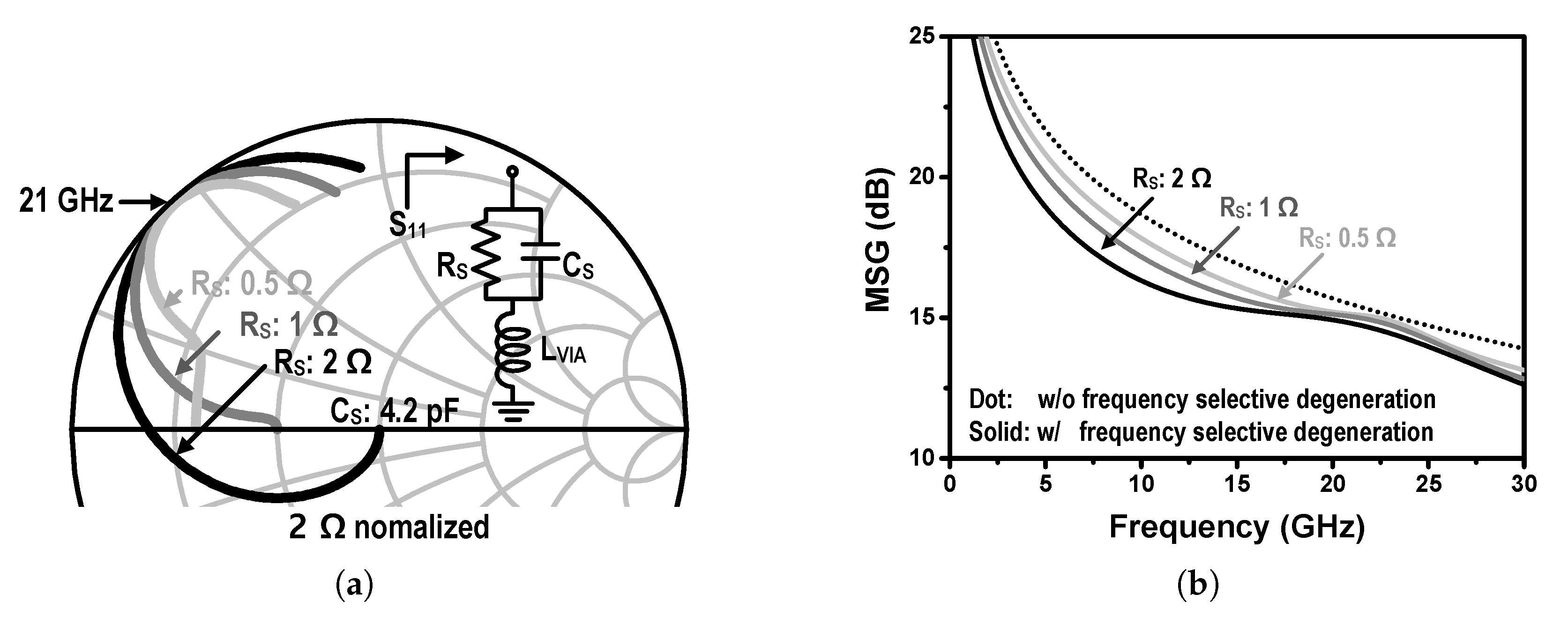
2. Design of the Proposed Broadband PAIC

Broadband PAIC should be designed to have uniform performances over a wide frequency band, which is very difficult because the gain of the transistor rapidly decreases as the frequency increases. A feedback and/or resistor biasing circuit have been conventionally used to reduce the gain at the low frequency without greatly reducing the gain of the high frequency band [2]. However, obtaining a very flat frequency response of the transistor over a wide frequency band is still a great challenge.
Figure 1 shows the source- and load-pull setup of the degenerated transistor with a resistance bias and feedback circuits for the proposed broadband PAIC. R F and C F are the series resistor and capacitor of the feedback circuits. R G is the resistor of the resistor bias circuit. The proposed frequency selective degeneration circuit consists of a resistor of R S , capacitor of C S , and an equivalent inductor of L V I A for the through-wafer via.
Figure 2a shows the frequency characteristics (S11) from DC to 30 GHz according to the capacitor values of the frequency selective degeneration circuit with a resistance of 1 Ω. According to the value of the capacitor, the frequency to have the real part of the impedance minimum (almost zero) shifts. Figure 2b shows the maximum stable gain (MSG) characteristics with various values of the capacitor in the frequency selective degeneration circuit. Increased power gain can be observed at the frequency that has a minimum resistance. For a 6–18 GHz broadband PAIC application, a slightly higher frequency of 21 GHz from the upper corner was selected to have a minimum degeneration with a capacitance of 4.2 pF.
Figure 3a shows the frequency characteristics (S11) from DC to 30 GHz according to the resistor values of the frequency selective degeneration circuit with a capacitance of 4.2 pF. Figure 3b shows the MSG characteristics, which shows that the level of degeneration can be controlled by the value of the resistor. The R S value for the proposed broadband PAIC design was optimized as 1 Ω. The simulated MSGs according to the frequency for the main stage are shown in Figure 4. Using the feedback and resistor bias circuits, the MSG value at the low frequency band can be somewhat reduced. Through the proposed frequency selective degeneration circuit, the MSG characteristics at low frequencies can be further reduced, while the MSG at high frequencies, especially for 21 GHz, can be very well maintained. As shown, the simulation results show that the flatter frequency response across the wide frequency band can be achieved. The drive stage can also be designed using the same structure as the main stage. The component values used in the design of the main and drive stages are presented in Table 1.

3. Experimental Results

Figure 5 shows the schematic diagram of the proposed broadband PAIC using the frequency selective degeneration circuit. The feedback, resistor biasing, and frequency selective degeneration circuits were simultaneously optimized to make the frequency response of the transistor as flat as possible. The proposed PAIC was designed with a two-stage and single-ended structure. The gate widths of the main and drive stages were 4 × 75 μ m and 2 × 75 μ m, respectively. The flat frequency response, as shown in Figure 4, allows the adoption of the single-section matching networks for small chip size. The output and inter-stage matching networks were designed with a high-pass structure, while the low-pass matching network was adopted at the input. The shunt inductor at the high-pass matching network was used to supply the DC voltage of 5 V to the drain. Figure 6 shows a photograph of the proposed broadband PAIC designed using Win Semiconductor’s 0.15 μ m GaAs pHEMT process, which provides an enhanced-mode GaAs PHEMT whose breakdown voltage is about 10 V. The quiescent currents of the main and drive stages were 64 mA and 41 mA, respectively.
Figure 7 shows the measurement results of the proposed 6 to 18 GHz GaAs pHEMT broadband PAIC. Figure 7a shows the measured S-parameters of the PAIC. For the 6 to 18 GHz band, S21 of 17.2 dB at 15 GHz, S11 of 9.15 dB or less, and S22 of 10.03 dB or less were measured. The flatness of S21 was ±1.1 dB in the band. The term ’flatness’ can be defined for gain and output power in the given frequency band as follows
f l a t n e s s = ± m a x i m u m v a l u e m i n i m u m v a l u e 2 .
The measurement results using a CW signal and a two-tone signal with a tone spacing of 10 MHz are shown in Figure 7b,c. Flatness of the saturated output power ±0.8 dB in the frequency band of 6 to 18 GHz was achieved. Power-added efficiency (PAE) of up to 20.3% was measured at the saturated output power of from 20.5 dBm to 22.1 dBm at the band. The output power that satisfies the IMD3 of 30 dBc was obtained in the range of 11.9 to 13.45 dBm, while the output power that satisfies the IMD3 of 40 dBc was obtained in the range of 7.8 dBm to 9.96 dBm. For the frequency band of 0 GHz to 30 GHz, the mu factor of no smaller than 1 can be observed from Figure 7d. Keysight’s advanced design system (ADS) for the circuit design and the momentum in ADS for electro-magnetic (EM) field simulation are used.
In Table 2, the measured performances were summarized and compared to the previously published broadband PAICs. The proposed broadband PAIC had the smallest chip size compared to the sizes of the PAICs presented in the previous works. It also had the best output power flatness, which was ±0.8 dB in the 6–18 GHz band. Compared to [1], this work clearly shows better performances in gain, gain flatness, input reflection, and output reflection characteristics. The proposed PAIC exhibited a higher PAE compared to [5]. In addition, this work reported the highest output power compared to the broadband PAICs designed with the GaAs pHEMT process.

4. Conclusions

In this paper, the frequency selective degeneration method for a 6 to 18 GHz GaAs pHEMT broadband PAIC was proposed. In order to achieve flatter frequency response of each stage, the feedback and resistor biasing circuits were used in addition to the frequency selective degeneration circuit. The level of degeneration and frequency range where the degeneration effect is minimized were controlled by optimizing the values of the capacitor and resistor in the frequency selective degeneration circuit. As a result, very flat frequency characteristics were achieved compared to the condition only using the feedback and resistor biasing circuits. The chip size was reduced by using single-section matching networks.
The proposed PAIC was designed using Win Semiconductor’s 0.15 μ m GaAs pHEMT process and had a size of 1.03 × 0.87 mm2. The fabricated PAIC has a two-stage and single-ended structure. It showed an average gain of 16.1 dB, gain flatness of ±1.1 dB, input reflection coefficient of no larger than 9.1 dB, and an output reflection coefficient of no larger than 10 dB in the frequency band of 6 to 18 GHz. The output power of 20.5 dBm to 22.1 dBm, output power flatness of ±0.8 dB, and PAE of from 12.4% to 20.3% were also experimentally obtained. It was experimentally verified that the proposed frequency selective degeneration circuit is beneficial to design broadband PAICs.

Author Contributions

Conceptualization, S.O., E.Y., and Y.Y.; Methodology, H.O.; Software, E.Y. and H.K.; Validation, S.O. and J.S.; Formal Analysis, K.C.H. and K.-Y.L.; Investigation, S.O. and E.Y.; Resources, E.Y.; Data Curation, S.O. and Y.Y.; Writing—Original Draft Preparation, S.O.; Writing—Review and Editing, S.O. and Y.Y.; Visualization, Y.Y.; Supervision, Y.Y.; Project Administration, Y.Y.; Funding Acquisition, Y.Y. All authors have read and agreed to the published version of the manuscript.

Funding

This work was supported by the National Research Foundation of Korea (NRF) grant funded by the Korea government (MSIT) (2018R1A2B3005479).

Conflicts of Interest

The authors declare no conflict of interest.

References

  1. Kerherve, E.; Demirel, N.; Ghiotto, A.; Larie, A.; Deltimple, N.; Pham, J.M.; Mancuso, Y.; Garrec, P. A Broadband 4.5–15.5-GHz SiGe Power Amplifier With 25.5-dBm Peak Saturated Output Power and 28.7% Maximum PAE. IEEE Trans. Microw. Theory Tech. 2015, 63, 1621–1632. [Google Scholar] [CrossRef] [Green Version]
  2. Lee, H.; Lee, W.; Kim, T.; Helaoui, M.; Ghannouchi, F.M.; Yang, Y. 6–18 GHz GaAs pHEMT Broadband Power Amplifier Based on Dual-Frequency Selective Impedance Matching Technique. IEEE Access 2019, 7, 66275–66280. [Google Scholar] [CrossRef]
  3. Jeong, J.; Yom, I.; Kim, J.; Lee, W.; Lee, C. A 6–18-GHz GaAs Multifunction Chip With 8-bit True Time Delay and 7-bit Amplitude Control. IEEE Trans. Microw. Theory Tech. 2018, 66, 2220–2230. [Google Scholar] [CrossRef]
  4. de Hek, P.; Van Caekenberghe, K.; van Dijk, R. A 3–14 GHz pseudo-differential distributed low noise amplifier. In Proceedings of the 5th European Microwave Integrated Circuits Conference, Paris, France, 27–28 September 2010; pp. 337–340. [Google Scholar]
  5. Santhakumar, R.; Thibeault, B.; Higashiwaki, M.; Keller, S.; Chen, Z.; Mishra, U.K.; York, R.A. Two-Stage High-Gain High-Power Distributed Amplifier Using Dual-Gate GaN HEMTs. IEEE Trans. Microw. Theory Tech. 2011, 59, 2059–2063. [Google Scholar] [CrossRef]
  6. Park, H.; Nam, H.; Choi, K.; Kim, J.; Kwon, Y. A 6–18-GHz GaN Reactively Matched Distributed Power Amplifier Using Simplified Bias Network and Reduced Thermal Coupling. IEEE Trans. Microw. Theory Tech. 2018, 66, 2638–2648. [Google Scholar] [CrossRef]
  7. Campbell, C.; Lee, C.; Williams, V.; Kao, M.Y.; Tserng, H.Q.; Saunier, P.; Balisteri, T. A Wideband Power Amplifier MMIC Utilizing GaN on SiC HEMT Technology. IEEE J. Solid-State Circuits 2009, 44, 2640–2647. [Google Scholar] [CrossRef]
  8. Oreja-Gigorro, E.; Pascual, E.D.; Sanchez-Martínez, J.J.; Gil-Heras, M.L.; Bueno-Fernandez, V.; Bodalo-Marquez, A.; Grajal, J. A 6–18 GHz GaN on SiC High Power Amplifier MMIC for Electronic Warfare. In Proceeding of the 13th European Microwave Integrated Circuits Conference (EuMIC), Madrid, Spain, 23–25 September 2018; pp. 85–88. [Google Scholar]
  9. Meghdadi, M.; Medi, A. Design of 6–18-GHz High-Power Amplifier in GaAs pHEMT Technology. IEEE Trans. Microw. Theory Tech. 2017, 65, 2353–2360. [Google Scholar] [CrossRef]
  10. Schmid, U.; Sledzik, H.; Schuh, P.; Schroth, J.; Oppermann, M.; Brückner, P.; van Raay, F.; Quay, R.; Seelmann-Eggebert, M. Ultra-Wideband GaN MMIC Chip Set and High Power Amplifier Module for Multi-Function Defense AESA Applications. IEEE Trans. Microw. Theory Tech. 2013, 61, 3043–3051. [Google Scholar] [CrossRef]
  11. Xia, Q.; Li, D.; Huang, J.; Li, J.; Chang, H.; Sun, B.; Liu, H. A 28 GHz Linear Power Amplifier Based on CPW Matching Networks with Series-Connected DC-Blocking Capacitors. Electronics 2020, 9, 617. [Google Scholar] [CrossRef] [Green Version]
  12. Lee, W.; Kang, H.; Lee, H.; Lim, W.; Bae, J.; Koo, H.; Yoon, J.; Hwang, K.C.; Lee, K.Y.; Yang, Y. Broadband InGaP/GaAs HBT Power Amplifier Integrated Circuit Using Cascode Structure and Optimized Shunt Inductor. IEEE Trans. Microw. Theory Tech. 2019, 67, 5090–5100. [Google Scholar] [CrossRef]
  13. Sharma, T.; Aflaki, P.; Helaoui, M.; Ghannouchi, F.M. Octave Bandwidth Doherty Power Amplifier Using Multiple Resonance Circuit for the Peaking Amplifier. IEEE Trans. Circuits Syst. I Reg. Pap. 2019, 66, 583–593. [Google Scholar]
  14. Kim, D.-M.; Kim, D.; Jeong, H.-G.; Im, D. A Reconfigurable CMOS Inverter-based Stacked Power Amplifier with Antenna Impedance Mismatch Compensation for Low Power Short-Range Wireless Communications. Electronics 2020, 9, 562. [Google Scholar] [CrossRef] [Green Version]
  15. Yang, Z.; Yao, Y.; Liu, Z.; Li, M.; Li, T.; Dai, Z. Design of High Efficiency Broadband Continuous Class-F Power Amplifier Using Real Frequency Technique With Finite Transmission Zero. IEEE Access 2018, 6, 61983–61993. [Google Scholar] [CrossRef]
  16. Lee, W.; Kang, H.; Choi, S.; Lee, S.; Kwon, H.; Hwang, K.; Lee, K.-Y.; Yang, Y. Scaled GaN-HEMT Large-Signal Model Based on EM Simulation. Electronics 2020, 9, 632. [Google Scholar] [CrossRef] [Green Version]
  17. Sharma, T.; Aflaki, P.; Helaoui, M.; Ghannouchi, F.M. Broadband GaN Class-E Power Amplifier for Load Modulated Delta Sigma and 5G Transmitter Applications. IEEE Access 2018, 6, 4709–4719. [Google Scholar] [CrossRef]
  18. Lee, S.; Park, H.; Choi, K.; Kwon, Y. A Broadband GaN pHEMT Power Amplifier Using Non-Foster Matching. IEEE Trans. Microw. Theory Tech. 2015, 63, 4406–4414. [Google Scholar] [CrossRef]
  19. Huang, C.; He, S.; Shi, W.; Song, B. Design of Broadband High-Efficiency Power Amplifiers Based on the Hybrid Continuous Modes With Phase Shift Parameter. IEEE Microw. Wirel. Compon. Lett. 2018, 28, 159–161. [Google Scholar] [CrossRef]
  20. Amirpour, R.; Darraji, F.; Ghannouchi, F.; Quay, R. Enhancement of the Broadband Efficiency of a Class-J Power Amplifier With Varactor-based Dynamic Load Modulation. IEEE Microw. Wirel. Compon. Lett. 2017, 27, 180–182. [Google Scholar] [CrossRef]
  21. Saad, P.; Hou, R.; Hellberg, R.; Berglund, B. A 1.8–3.8-GHz Power Amplifier With 40% Efficiency at 8-dB Power Back-Off. IEEE Trans. Microw. Theory Tech. 2018, 66, 4870–4882. [Google Scholar] [CrossRef]
  22. Liu, B.; Mao, M.; Khanna, D.; Boon, C.; Choi, P.; Fitzgerald, E.A. A Novel 2.6–6.4 GHz Highly Integrated Broadband GaN Power Amplifier. IEEE Microw. Wirel. Compon. Lett. 2018, 28, 37–39. [Google Scholar] [CrossRef]
Figure 1. Source- and load-pull setup for the proposed broadband power amplifier integrated circuit (PAIC).
Electronics 09 01588 g001
Figure 2. Frequency characteristics according to the capacitor values with a resistance of 2 Ω, (a) S11 for the frequency selective degeneration circuit, (b) maximum stable gain (MSG) of the transistor.
Electronics 09 01588 g002
Figure 3. Frequency characteristics according to the resistor values with a capacitance of 4.2 pF, (a) S11 for the frequency selective degeneration circuit, (b) MSG of the transistor.
Electronics 09 01588 g003
Figure 4. Simulated MSGs of the main stage with optimized resistance and capacitance of 1 and 4.2 pF for the degeneration circuit, respectively.
Electronics 09 01588 g004
Figure 5. Overall schematic diagram of the proposed broadband PAIC.
Electronics 09 01588 g005
Figure 6. Overall schematic diagram of the proposed broadband PAIC.
Electronics 09 01588 g006
Figure 7. Experimental results of the proposed 6–18 GHz GaAs pHEMT broadband PAIC, (a) small-signal S-parameters, (b) saturated output power and PAE, and (c) linear output power with an IMD3 of 30 dBc and 40 dBc, (d) mu factor.
Electronics 09 01588 g007
Table 1. Component values for the feedback, resistor bias, and frequency selective degeneration circuits.
Main StageDrive Stage
R F C F R G R S C S R F C F R G R S C S
200 Ω1 pF50 Ω1 Ω4.2 pF300 Ω1 pF126 Ω1 Ω4.2 pF
Table 2. Component values for the feedback, resistor bias, and frequency selective degeneration circuits.
Ref.ProcessFreq.
(GHz)
Gain *
(dB)
Gain Flatness
(dB)
Input Reflection **
(dB)
Output Reflection **
(dB)
P out ***
(dBm)
P out Flatness
(dB)
PAE
(%)
Size
(mm2)
Structure
[1]0.13 μ m SiGe
BiCMOS
4.5–15.513.8±2.8 5.0 2.3 21.3±2.111.9–28.71.96Cascode differential
[5]0.2 μ m GaN
HEMT
2.0–18.019.5±1.5 14.0 + 5.0 +26.0±2.05.0–12.08.0Distributed
[4]0.15 μ m GaAs
pHEMT
3.0–14.017.0±1.0 15.0 10.0 15.0--7.44Distributed
[3]0.25 μ m GaAs
pHEMT
6.0–18.012.0±1.0 10.0 + 10.0 +15.0±1.5-5.2Two-stage
[2]0.15 μ m GaAs
pHEMT
6.0–18.017.4±1.0 8.0 +-19.2±0.913.0–21.70.97Two-stage
This work0.15 μ m GaAs
pHEMT
6.0–18.016.1±1.1 9.1 10.0 20.5±0.812.4–20.30.89Two-stage
* median value; ** maximum value; *** minimum value; + graphically estimated.

