Article

The Study of the Operational Characteristic of Interleaved Boost Converter with Modified Coupled Inductor

Department of mechatronics and electronics, Faculty of electrical engineering and information technologies, University of Zilina, Univerzitna 1, 010 26 Zilina, Slovakia
*
Author to whom correspondence should be addressed.
Electronics 2019, 8(9), 1049; https://doi.org/10.3390/electronics8091049
Submission received: 12 August 2019 / Revised: 5 September 2019 / Accepted: 16 September 2019 / Published: 18 September 2019
(This article belongs to the Section Power Electronics)

Abstract

:
In this article, design, analysis, and experimental testing of a dual interleaved boost converter with coupled inductor including demagnetizing winding are presented. Proposed topology uses the specific design of boost coils placed within the side parts of the EE core together with a demagnetizing coil located on the center part of the core. Paper describes principles of operational scenarios and characteristics. Through modification of turns ratio between boost coils and demagnetizing coil is possible to achieve high voltage gain. Consequently, the functional performance of this perspective topology is realized experimentally. For that purpose, the physical sample of converter is designed and tested in terms of efficiency considering the change of transferred power or the change of input voltage. Through modification of turns ratio between boost coils and demagnetizing coil is possible to achieve high voltage gain, therefore these dependencies are also evaluated considering also the change of the duty cycle. At the end of the paper basic operational properties are compared to standard boost topologies. It was discovered that even due to higher complexity of the proposed converter oppose to selected topologies, the operational performance is much better considering ripple of the electrical variables, efficiency, or the size of circuit components.

1. Introduction

Nowadays, in many power conversion applications, the boost converters (isolated or non-isolated) are used. The most important parameter of every power converter is high efficiency, low costs, and low volumes [1,2,3].
Due to the limited resources of fossil fuels and also their serious environmental impacts including greenhouse gas emissions, global warming, and environmental pollution, the renewable technologies such as photovoltaic (PV) systems, fuel cells have received extensive attention as a clean source of energy [4,5,6,7,8,9] similarly current trends in automotive applications are characterized by a common rule-green energy, or blue energy [10,11,12,13]. High gain DC/DC (direct current to direct current) converters are the key part of renewable energy systems. The designing of high gain DC/DC converters is imposed by severe demands. Designers face contradictory constraints such as low cost and high reliability. First of all, the inverters must be safe in terms of further maintenance as well as in relation to the environment [14,15,16,17].
For almost all industrial and commercial applications the power consumption increases continuously thus it becomes impossible for a single-phase converter to withstand the high current stress [18,19,20]. One of the ways how to optimize this negative characteristic is a connection of converter cells in parallel instead of paralleling switching devices of a single cell [21]. The multiphase interleaved converters thus have benefits related to better transient response, power scalability, and better light load efficiency [22,23,24]. The single-phase converter uses large inductance, which limits the dynamics of the energy transfer within the main circuit [25]. To increase the transient response of the inductor, the value of inductance needs to be reduced significantly. On the other side, small inductance results in large current ripple. The large current ripple usually causes a large turn-off loss and generates large voltage ripple on the input capacitor that is comparable to transient voltage spikes [25,26,27,28,29]. Due to above-mentioned facts the use of the interleaved technique with several converter cells whose inductance value is reduced results in quick and efficient power transfer from input to the output. Improvements of some properties have been achieved in dual interleaved boost (DIB) converters with coupled inductors [30,31,32], or with voltage lift technique have been proposed.
Electrical behavior of power stage of switched-mode power supplies based on interleaved solution still provides several disadvantages. Those are mostly related to power limitations and voltage gain limitations. High power levels are mostly problematic, because of the increase of conduction losses within the circuit together with a high increase of magnetic components losses, which are related to the DC biasing and consequently components saturation [32,33,34]. Careful attention shall be paid on the magnetic component design, while there are several proposals how to overcome the negative consequences of the interleaved topologies [35,36,37].
Anyway, within presented research approach attention is given on further optimizations of the magnetically coupled inductor, which is one of the main parts of double-interleaved boost inductor. The investigated topology consists of two interleaved boost converters whose operation is shifted by 180° phase delay. Boost inductors are placed on side parts of the ferrite core. Together with boost inductors additional two SiC diodes are being used for connection with a demagnetizing inductor. The output capacitor is then supplied through another two diodes, thus 4 diodes are required for proper operation of the converter. Due to the addition of demagnetizing inductor, it is possible to achieve voltage gain whose value can be adjusted also by the turn’s ratio between boost and demagnetizing inductors. This topology is primarily suited for the applications, where high efficiency, adjustable voltage gain and low dimensions are required, while galvanic isolation between input and output is not required.
Within the presented paper, the analysis of the main circuit operation is being shown, while the focus is given on the operational intervals for various scenarios of the duty cycle value. Consequently, magnetic circuit of coupled inductor with demagnetizing coil is described, while identification of coupling coefficient is done for the needs of the simulation experiments. At the end of the paper, more detailed analysis is provided on the experimental sample of proposed converter (500 W), while the dependency of voltage gain on duty cycle and turns ration is given. Also, efficiency performance is being investigated within various operational conditions. Finally, critical comparison to other standard DIB and boost converters is given.

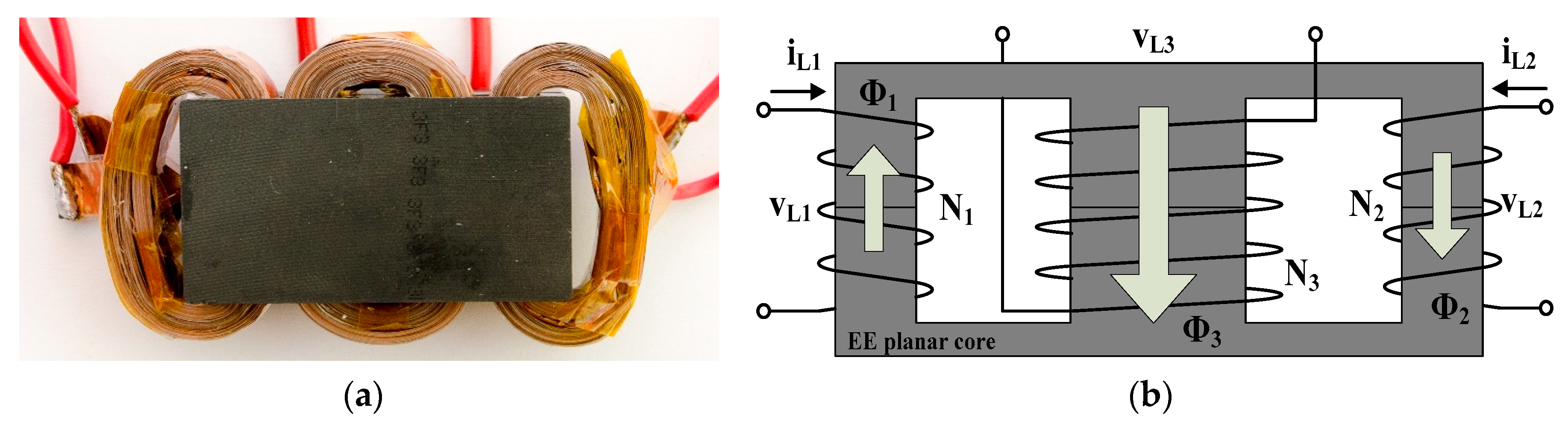
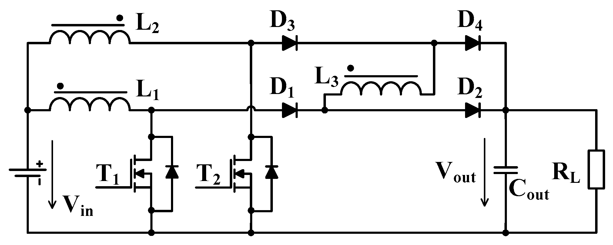
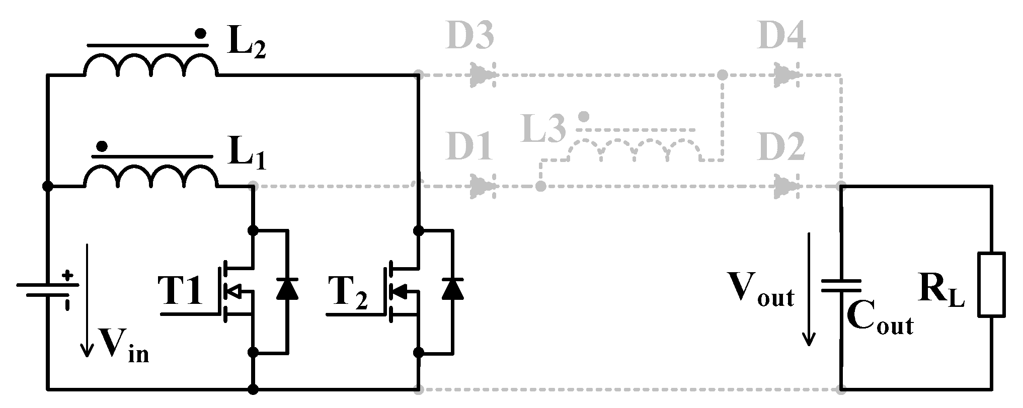
2. Dual Interleaved Boost with Coupled Inductors

Figure 1 shows a schematic diagram of the proposed interleaved converter with a coupled inductor. The proposed converter consists of T1, T2 transistors, coupled L1, L2, and demagnetizing L3 inductors, filtering capacitor COUT and diodes D1–D4. The proposed converter is derived from standard interleaved boost converter by adding third inductor and two rectifiers diode. Coil L3 is magnetically coupled with L1 and L2 on the common magnetic core. The reason for the use of L3 is related to the possibility of DC flux reset of the ferrite core. Switching of the transistors is similar to standard interleaved boost converter, thus 180° phase shift between gate drive impulses applies. On the other side, the duty cycle range can be extended for both transistors up to D = 100%. The benefit of the proposed topology compared to the standard is that the inductors L1 and L2 are periodically demagnetized during operation, so the saturation of the core is reduced. This effect is made by the presence of L3 within the converter´s main circuit.
Main circuit component i.e. coupled inductor is wound on the common ferrite core E43 which is planar type. The windings of individual coils are made of copper foil. Figure 2 shows the designed component together with its equivalent circuit and winding directions of L1, L2, L3. The equivalent magnetic circuit shown in Figure 2b shows also the direction of the magnetic fluxes Φ1–Φ3, which are caused by the inductor currents iL1–iL3.

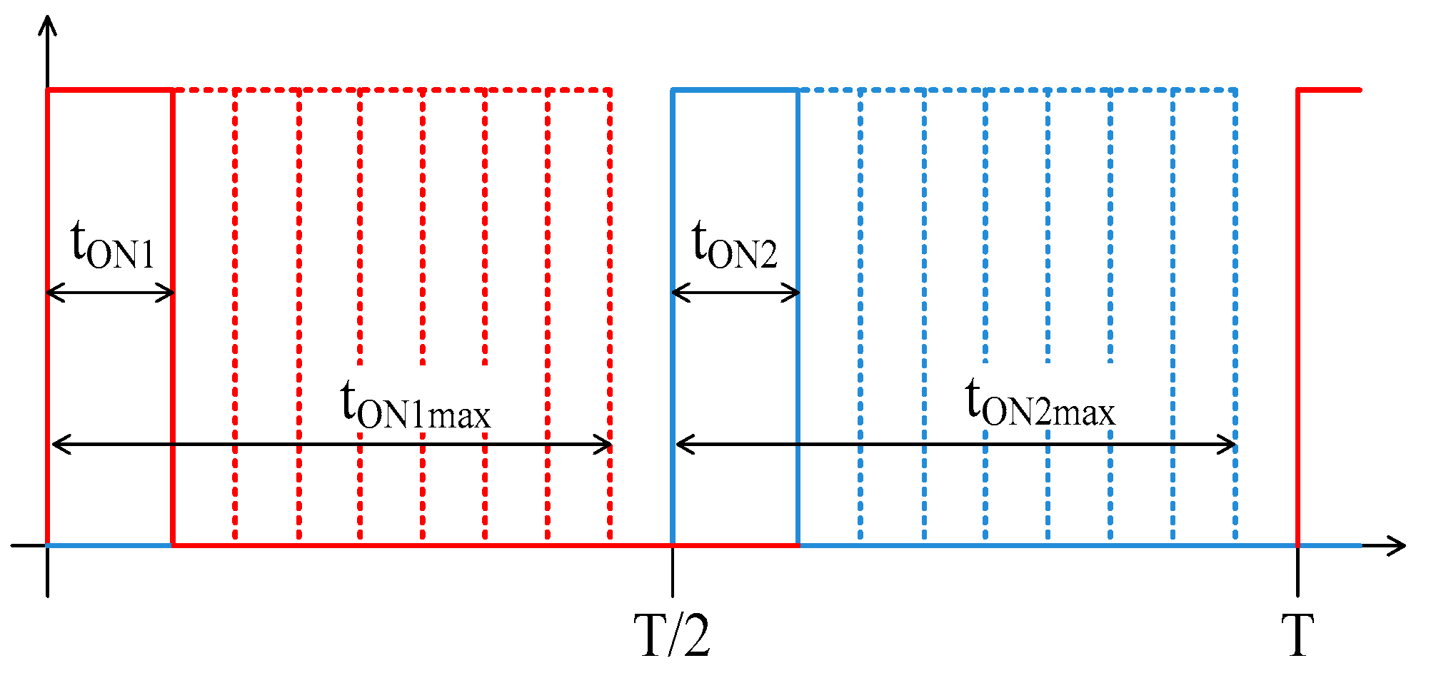
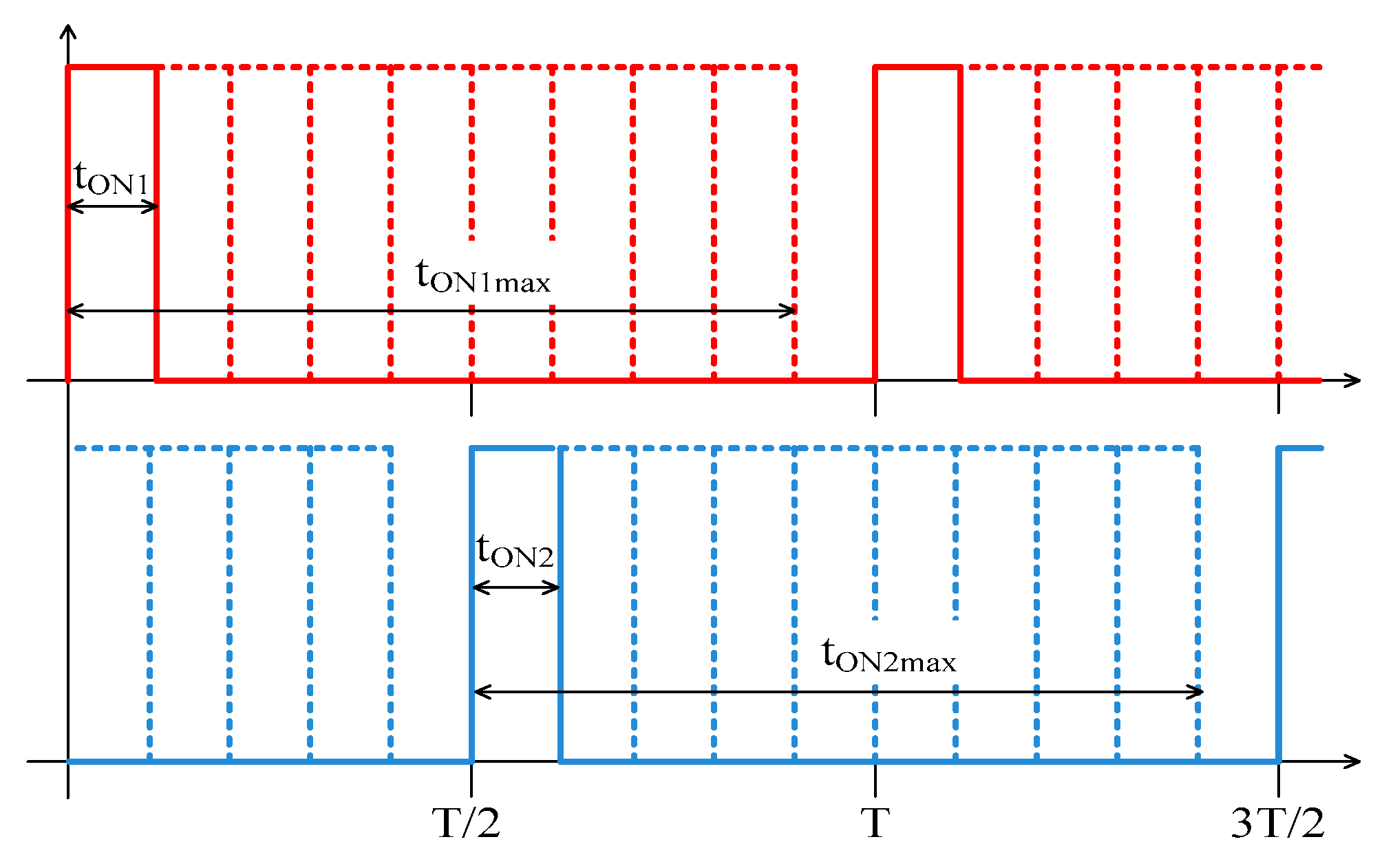
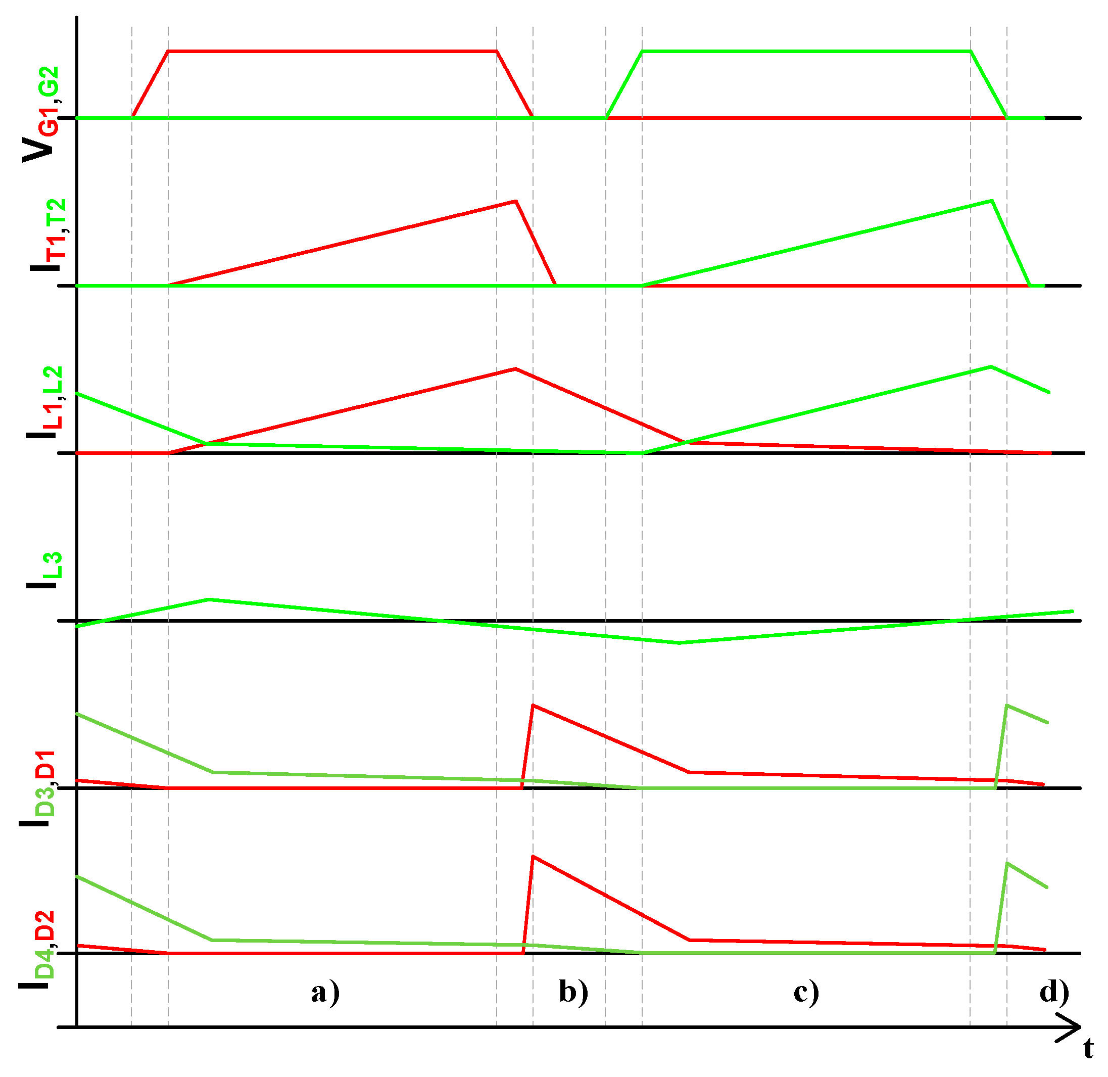
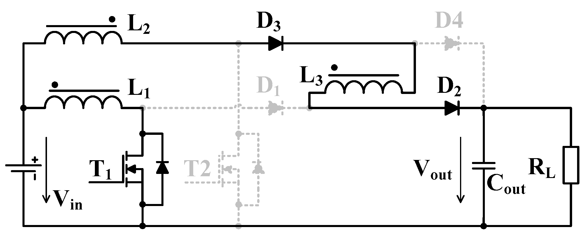
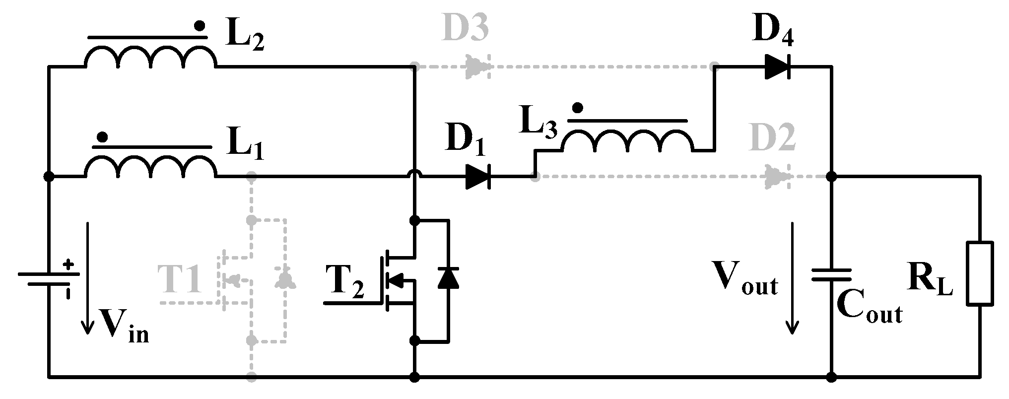
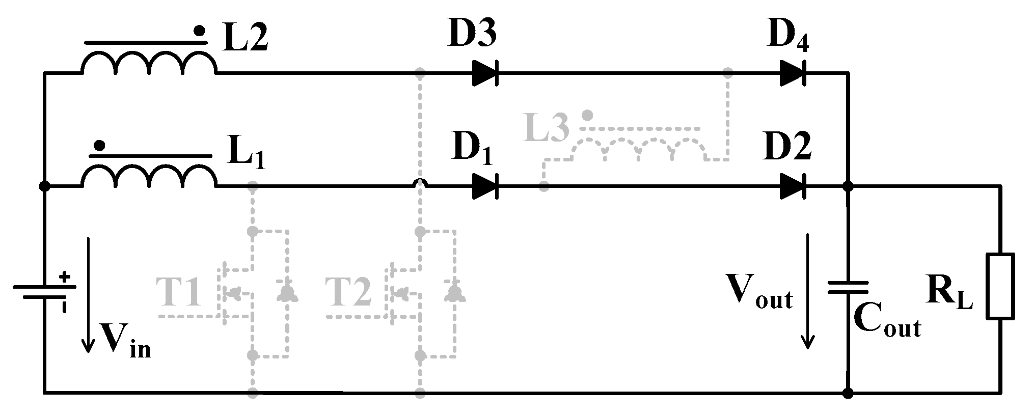
2.1. Analysis of the Operational Intervals

As was mentioned the converter operation can be realized with various duty cycle range, i.e. for D < 50% and for D > 50%. Gate drive impulses during both states are shown in Figure 3 and Figure 4 respectively. Within this paper two situations are analyzed for converter operation, D = 35% and for D = 65%. It is expected that the converter behavior for both operational states will be different.
The proposed converter operates within four main intervals of conduction while the duty cycle is below 50% (Figure 5). These intervals repeat periodically every switching period.
a) Interval: Transistor T1 is ON, T2 is OFF, The T1 and L1 currents are linearly increasing, The L3 and D3, D4 currents are linearly decreasing.
b) Interval: Transistor T1 is OFF, T2 is OFF, The L1 current is linearly decreasing and energy from L1 are sinking to the load trough the D1 and D2.
c) Interval: Transistor T1 is OFF, T2 is ON, The T2 and L2 currents are linearly increasing, The L3 and D1, D2 currents are linearly decreasing.
d) Interval: Transistor T1 is OFF, T2 is OFF, The L2 current is linearly decreasing and energy from L2 is sinking to the load trough the D3 and D4.
Figure 6 shows the principal waveforms of the converter variables for the situation when the value of the duty cycle exceeds 50%. For this case D = 65% was used.
a) Interval: Transistor T1 is ON, T2 is ON, the L1 and L2 currents are linearly increasing, the L3 current are linearly increasing and D1 current is linearly decreasing.
b) Interval: Transistor T1 is ON, T2 is OFF, the L1 current is linearly increasing and energy from L2 is sinking to the load trough the D2 and D3.
c) Interval: Transistor T1 is ON, T2 is ON, the L1 and L2 currents are linearly increasing, the L3 current are linearly decreasing and D2 current is linearly decreasing.
d) Interval: Transistor T1 is OFF, T2 is ON, the L2 current is linearly increasing and energy from L1 are sinking to the load trough the D1 and D4.
The induced voltage in each of the three windings is defined as follows:
v L 1 = N 1 d Φ 1 d t v L 2 = N 2 d Φ 2 d t v L 3 = N 3 d Φ 3 d t
where: vL1, vL2 and vL3 are the winding voltages; N1, N2, and N3 are the numbers of turns of each winding L1, L2, and L3, respectively, and Φ1, Φ2, and Φ3 are the magnetic fluxes interlinking with the windings L1, L2, and L3, respectively. Moreover, for the symmetry between the two phases, we assume N12=N1=N2. Additionally, according to Figure 2 we have:
Φ 3 = Φ 1 Φ 2
the induced voltage in the central winding:
v L 3 = N 3 ( v L 1 v L 2 ) N 12
Next, we introduce N as the ratio of the number of turns of the central winding and the number of turns of L1 or L2:
N = N 3 N 12
Finally, substituting (4) into (3), we can get the induced voltage in the central winding in the function of the voltage of L1 and L2:
v L 3 = N ( v L 1 v L 2 )

2.2. Steady-State Analysis

The steady-state analysis is performed for both situations of the converter operation, i.e. when duty – cycle operation is considered below and above 50% (Figure 3, Figure 4, Figure 5 and Figure 6). For these purposes just, equivalent circuits are selected which are cyclically repeated.

2.2.1. 1st Mode (1st Conduction Interval)

T1 is turned ON and T2 is turned OFF. During this interval, the energy is accumulated within the magnetic core of L1, while the L2 supports the output current flow through D3-L3-D2. The value of the current flowing through L2-D3- L3-D2 is decreasing and its maximal value is limited by the value of magnetizing current, which is determined by the mutual relationship between L2-L3. This interval ends when dead-time between switching of T1 and T2 is applied.
Considering this operational interval, we can define the input voltage of the converter as follows:
v I N = N 12 Δ Φ 1 T 1
Under the assumption of (1) and (2) and based on the situation given by the equivalent circuit from Figure 7 the input and output voltage dependency can be defined by (7).
v I N = N 12 Δ Φ 2 T 1 N 3 Δ Φ 3 T 1 + V o u t
where and ΔΦ1, ΔΦ2 and ΔΦ3 are the magnetic flux variations in the windings L3, L2 and L3 and T1 is the time duration of Mode 1, vIN is input voltage, Vout output voltage.

2.2.2. 2nd Mode (2nd Conduction Interval)

T1 turned OFF and T2 is turned ON. The beginning of this interval is characterized by the current iL1 decrease to the value of the magnetizing current. From this point the visible increase of iL2 is evident. L1 is supporting the output with current flow through D1-L3-D4. The current direction of the iL3 is opposite to iL1 thus the demagnetizing ability of the proposed magnetic component is clear. The interval ends similarly as 1st Mode of operation, i.e. before dead-time.
Considering this operational interval (Figure 8), we can define the value of input voltage of the converter based on the (7), while the end of the 1st interval represents initialization of the 2nd interval:
v I N = N 12 Δ Φ 1 T 2 N 3 Δ Φ 3 T 2 + V o u t
Under the assumption of (1) and (2) the value of the input voltage can be expressed by (9).
v I N = N 12 Δ Φ 2 T 2
where T2 is the time duration of Mode 2.

2.2.3. 3rd Mode (Dead-Time)

T1 and T2 are turned OFF (Figure 9). This interval is the so-called dead-time and is valid just and only during operation if the duty cycle is below 50%. During this interval, the commutation between the transistor and diodes is occurring. Also, one of the main inductances (L1, L2) is de-energized to the value of the magnetizing current, while supporting the output current.
Similar to the previous situation from 2nd operational interval, the value of the input voltage, or the dependency between input–output situation shall be expressed under the assumption of (3) and (4) as follows:
v I N = N 12 Δ Φ 1 T 3 + V o u t
v I N = N 12 Δ Φ 2 T 3 + V o u t
where T3 is the time duration of Mode 3.

2.2.4. 4th Mode (Valid Only for Duty > 50%)

T1 and T2 are turned ON and the inductors L1 and L2 are accumulating the energy within their magnetic circuits. The output is supported just by the energy stored in COUT.
The condition within this operational interval can be described by the situation which is valid from 3rd operational interval while considering the equivalent circuit from Figure 10 is given by the next equations:
v I N = N 12 Δ Φ 1 T 4
v I N = N 12 Δ Φ 2 T 4
where T4 is the time duration of Mode 4.

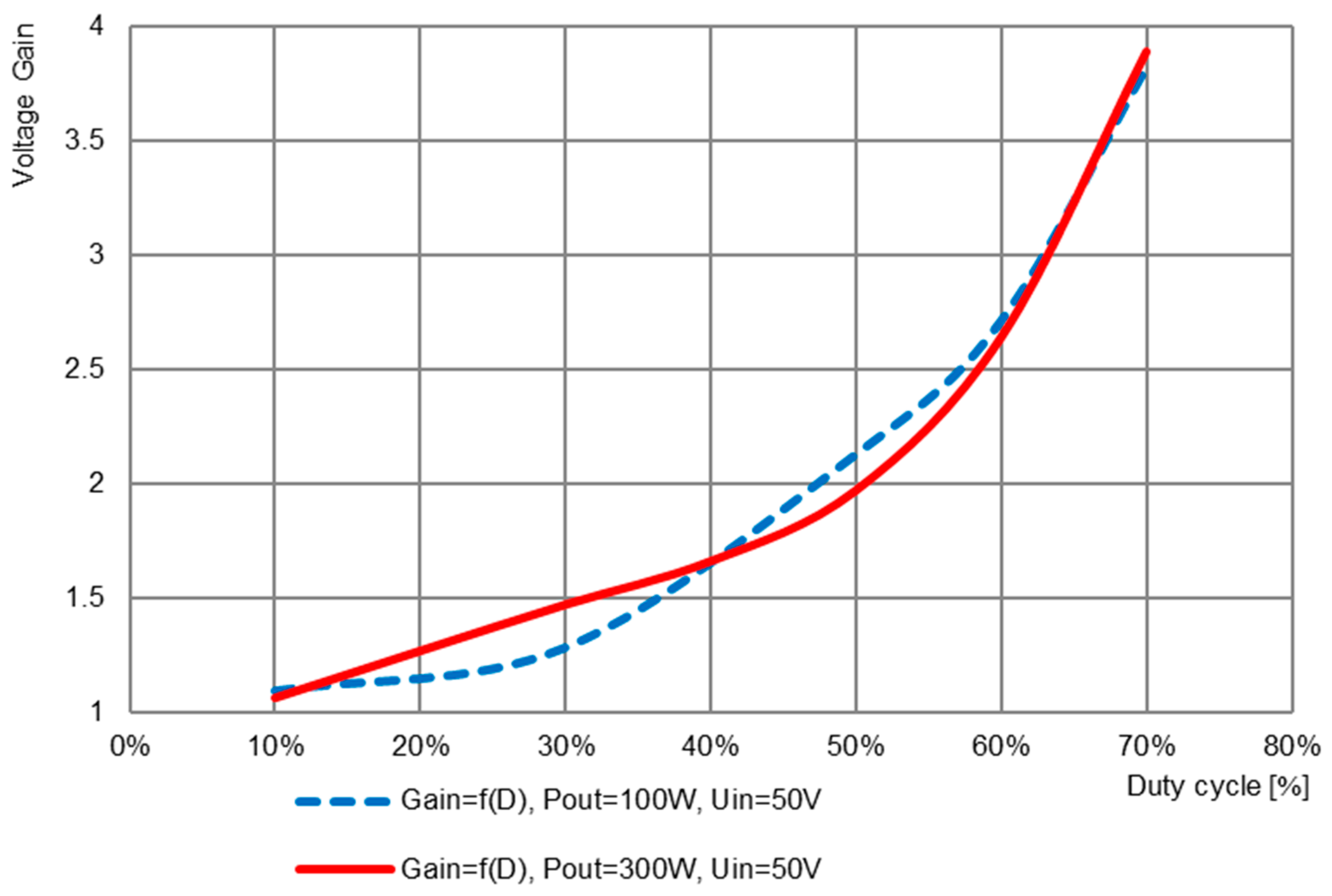
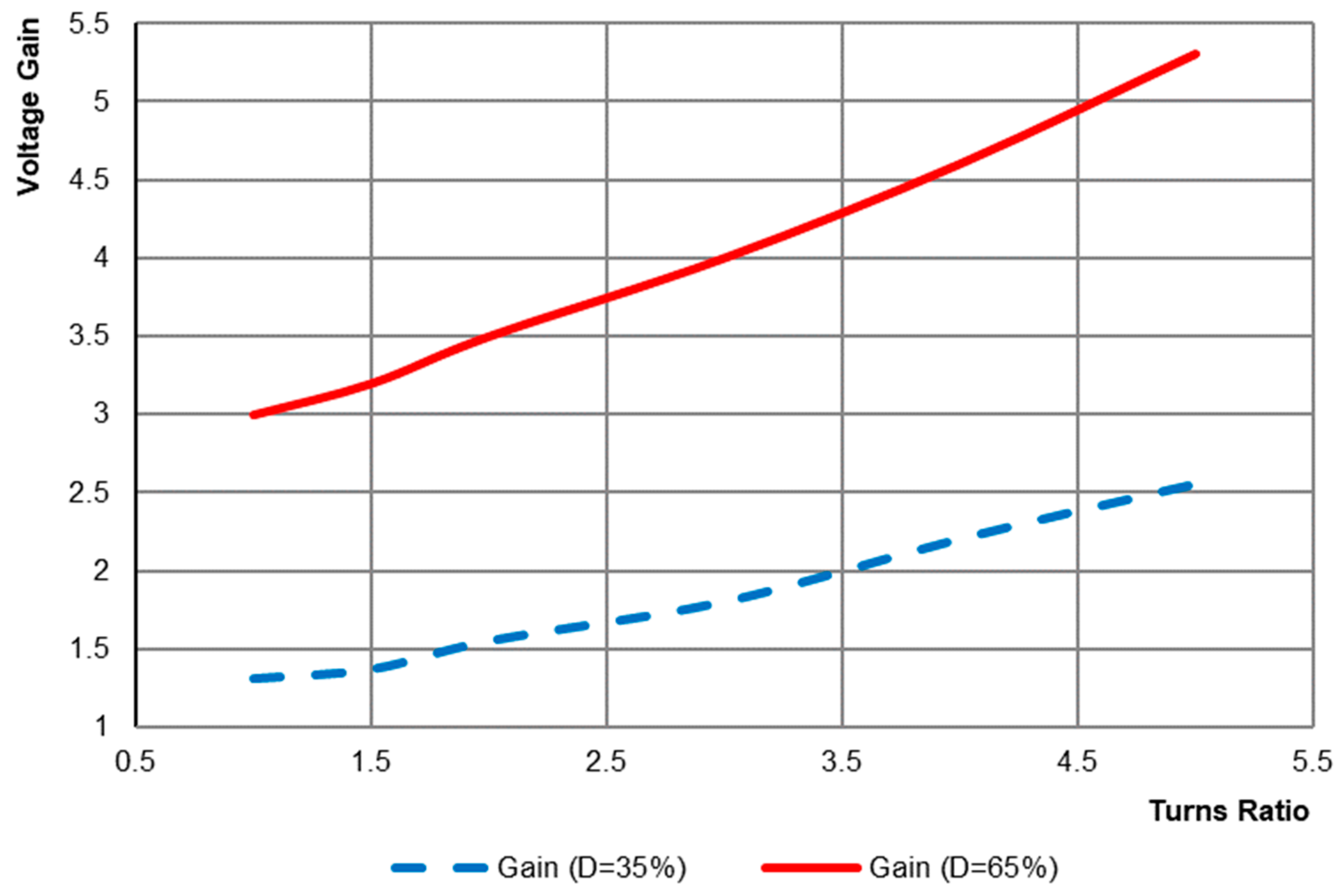
2.3. Voltage Gain Calculation

The voltage gain M, defined as the ratio of the output and input of voltage in dependence on the value of the duty cycle D when it is lower than 50% can be obtained from (6), (8), and (10) and is derived as follows:
M D 0.5 = 1 + N ( 1 + N ) D ( 1 + 2 N )
The voltage gain when the duty cycle is higher than 50% is expressed as:
M D 0.5 = 1 + N ( 1 D )

2.4. Determination of Coupling Coefficients Between the Coils

For the purposes of simulation investigation as well as for optimization purposes of the magnetic design of coupled inductor with the demagnetizing coil, the coupling coefficients of the converter shall be determined. The process of the identification was realized experimentally, initially through measurement of parasitic DC resistance and inductance of individual coils—Table 1.
Consequently, mutual inductances have been measured between coils L1 and L2 for coincident and anti-coincident directions of the coil windings (Figure 11). The measured values of mutual inductances are listed in Table 2.
Measured values of the mutual inductances have been used for the determination of the coupling coefficients, what is given by (16)–(18).
M 12 N = L 1 + L 2 L 12 N 2
M 12 P = L 12 P L 1 L 2 2
k 12 M 12 L 1 * L 2
Based on the (18) including individual values of inductances, the coupling coefficients have been determined (Table 3).

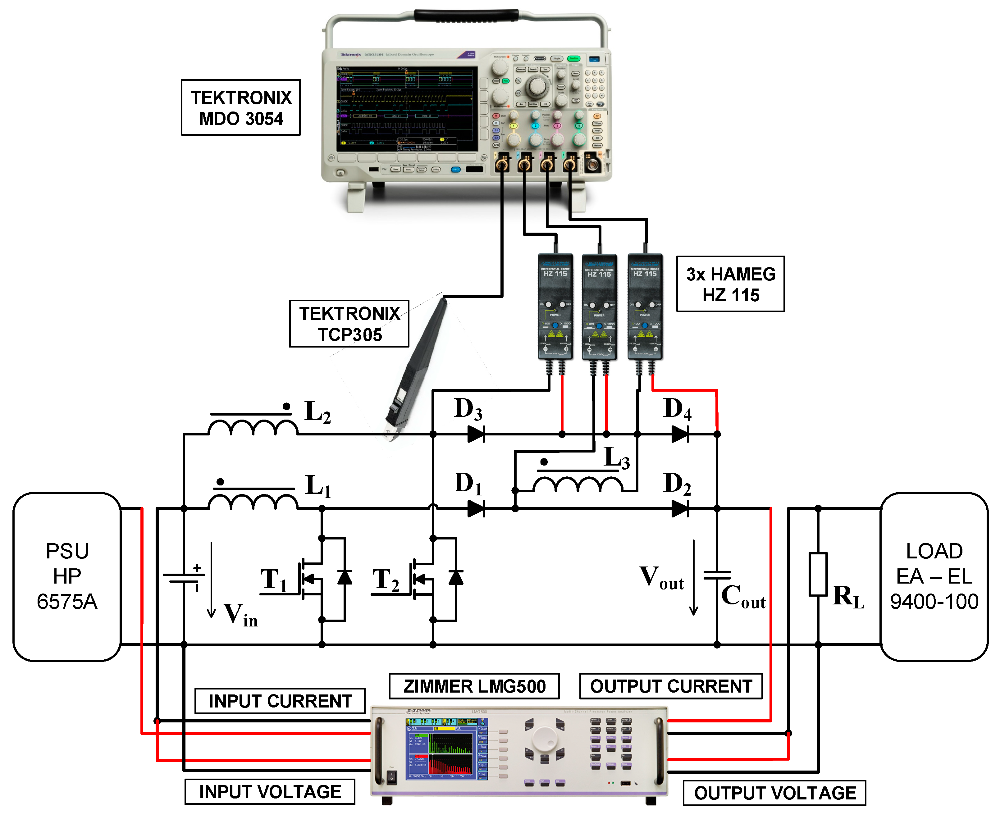
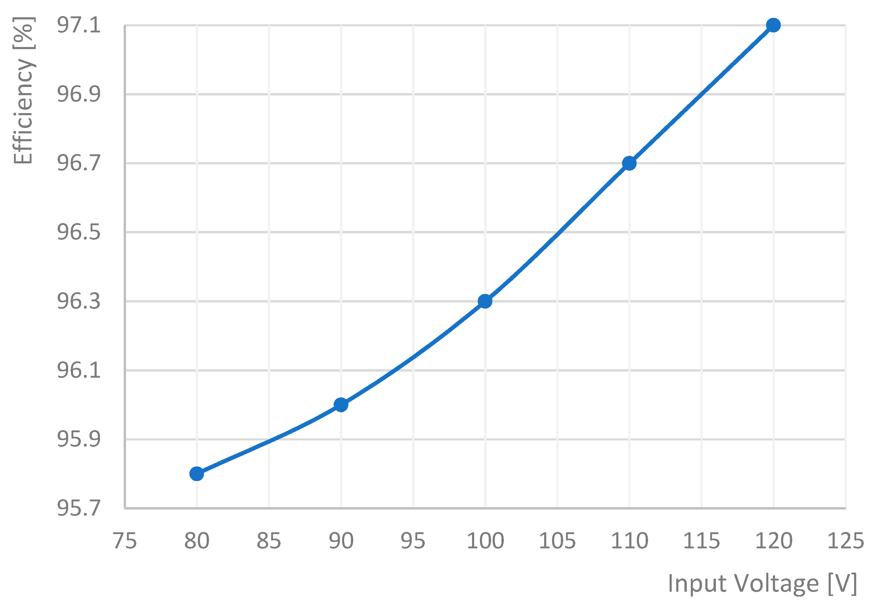
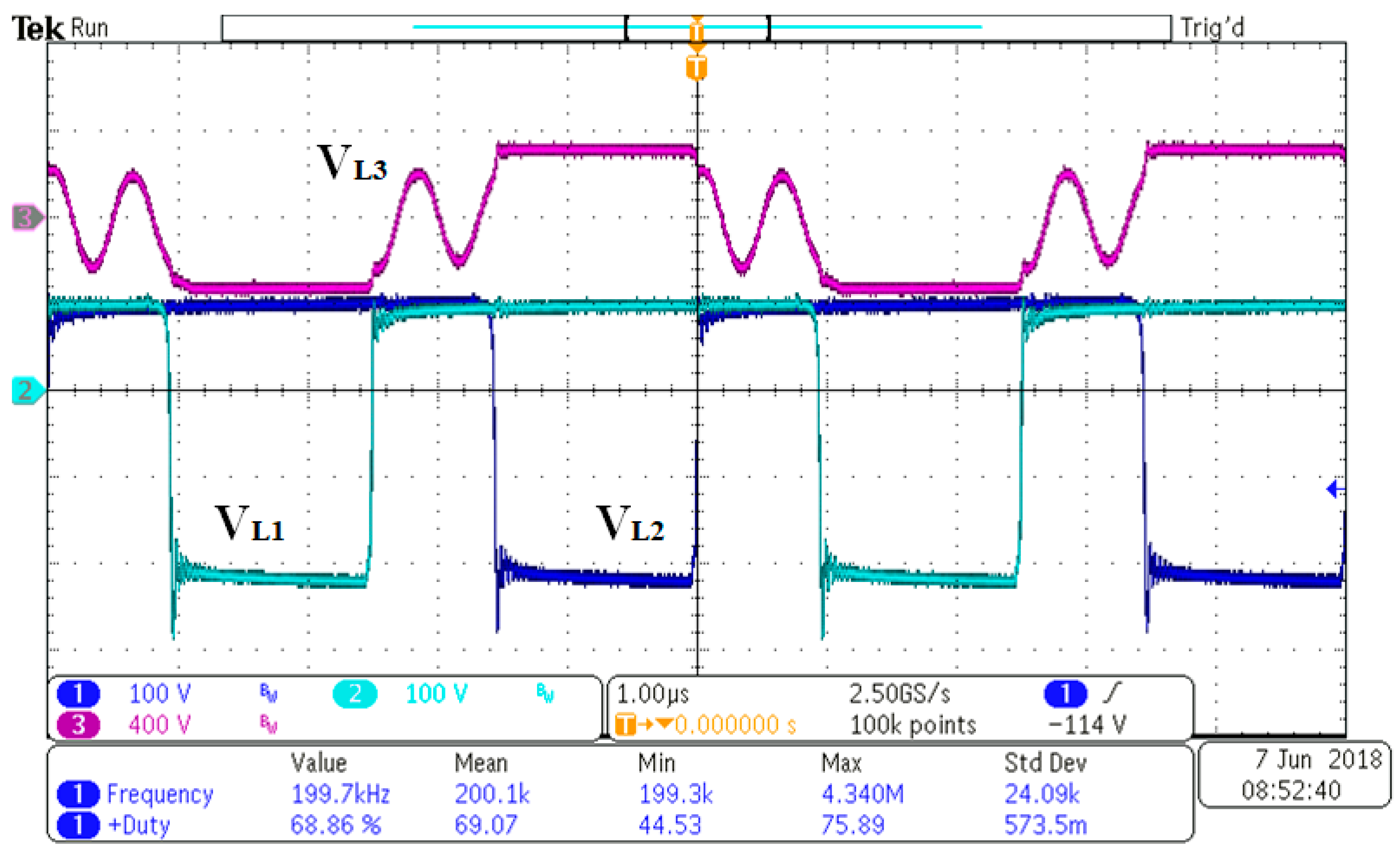
3. Experimental Verification

Experimental measurements have been realized on the converter prototype sample (Figure 12), whose main circuit parameters are listed below. Main circuit parameters were selected for the application use within photovoltaic systems, where proposed converter solutions shall be used as MPPT converter, which shall distribute energy within other power semiconductor converter subsystems or shall operate as energy charger for storage components (Figure 12). Also, these parameters have been selected due to the ability of photovoltaic panels which are connected in series, while their output voltage is reaching 120 V [38]. Since the converter system considers microgrid operation its power rating was initially set to 500 W, while it is not excluded that other variations of input/output parameters are not possible.
The focus was given on the investigation of the converter operation with a duty cycle above and below 50%. For the operation D < 50%, value of the duty cycle was set to 35% and for D > 50% value of the duty cycle was 65%. Initially, the time waveforms on the inductors were investigated due to verification of the existence of AC magnetic flux of the L3, which serves for the core demagnetization. Finally, the focus was given on the evaluation of the efficiency and voltage gain performance for the selected duty cycle values [39,40,41,42]. At this point the turns ratio between L1 and L2 is equal to 1:1, while the turns ratio between L1 and L3 and L2 and L3 is 1:1,7.
-
Input voltage = 100 V
-
Switching frequency (fSW) = 200kHz
-
Output voltage = 300 V
-
Output power = 500 W
-
Duty cycle = D1 = D2 = range 0–95%
-
Turns ratio = 3.6 (N1=N2 = 6, N3=10 => TR = 1:1.7)
Figure 13 shows the arrangement of the experimental set-up, which was prepared for the individual measurements. For the time-waveform measurement of the circuit components, the oscilloscope MDO3054 was used, while evaluation of the efficiency and other circuit variables (input–output voltages) for the purpose of graphical dependencies were recorded with the use of spectral analyzer Zimmer LMG500.

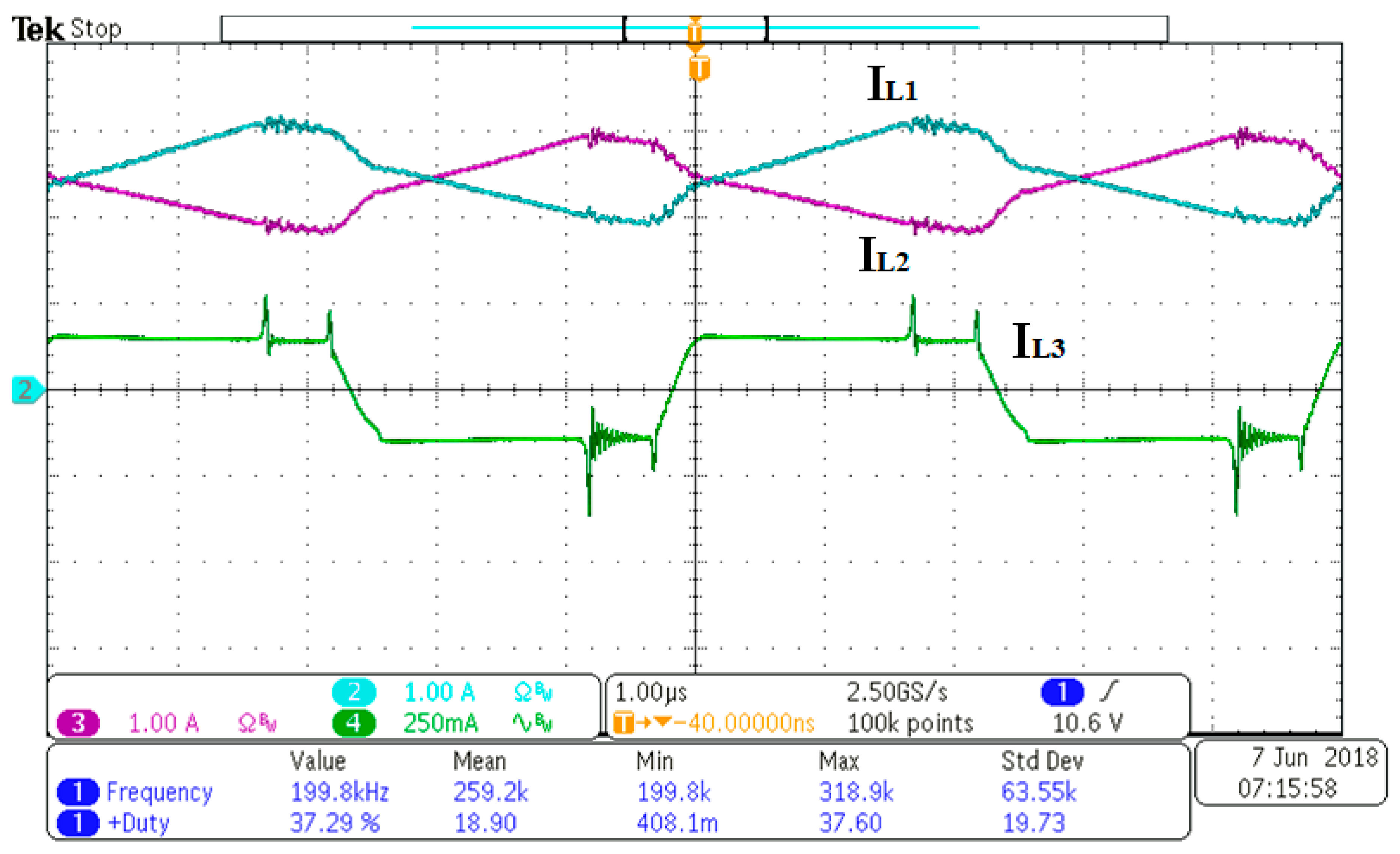
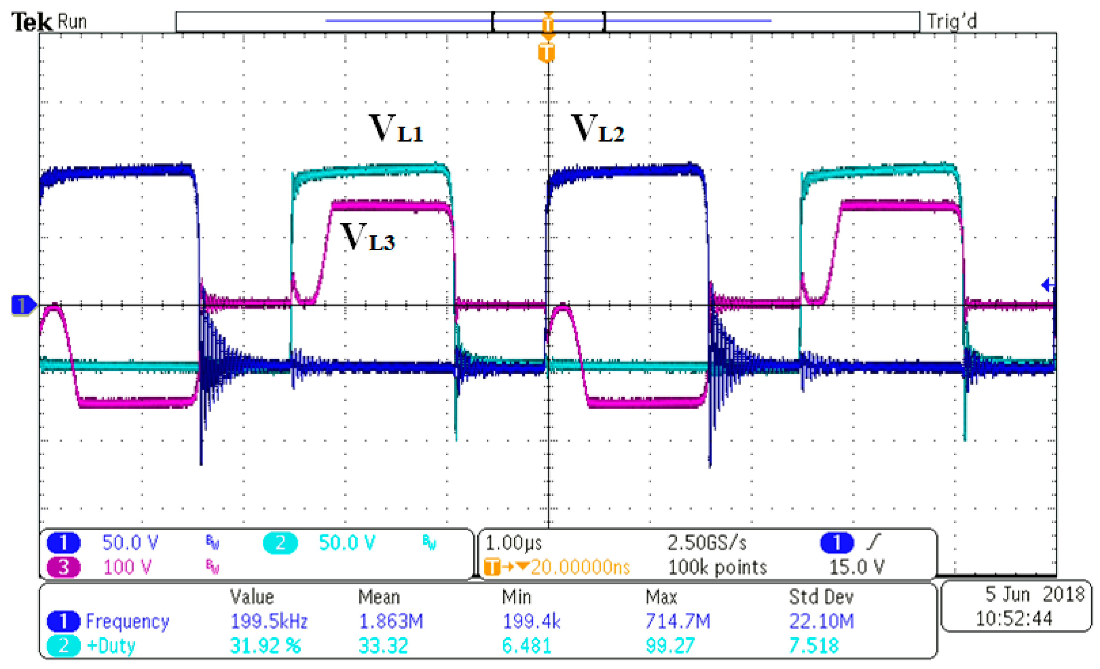
3.1. Measurement Results for D < 50% (35%)

Figure 14 shows the time-waveforms of the inductors currents during the operation when D = 35%. It is seen, that the current of the L3 coil has an AC character within the selected operating range. Dead-time is visible through the waveform of IL1 and IL2 when the character of these currents is decreasing. The received waveforms correspond to the theoretical operation described in Figure 5.
Figure 15 shows the time waveforms of the inductance voltages and the character of voltage VL3 is exhibiting alternating shape. The small valleys at the begin of each period are caused due to the dead-time existence during operation.
Based on the results from Figure 14 and Figure 15 is seen, that the shapes of the waveforms are without significant disturbances thus the converter operation acts stable.

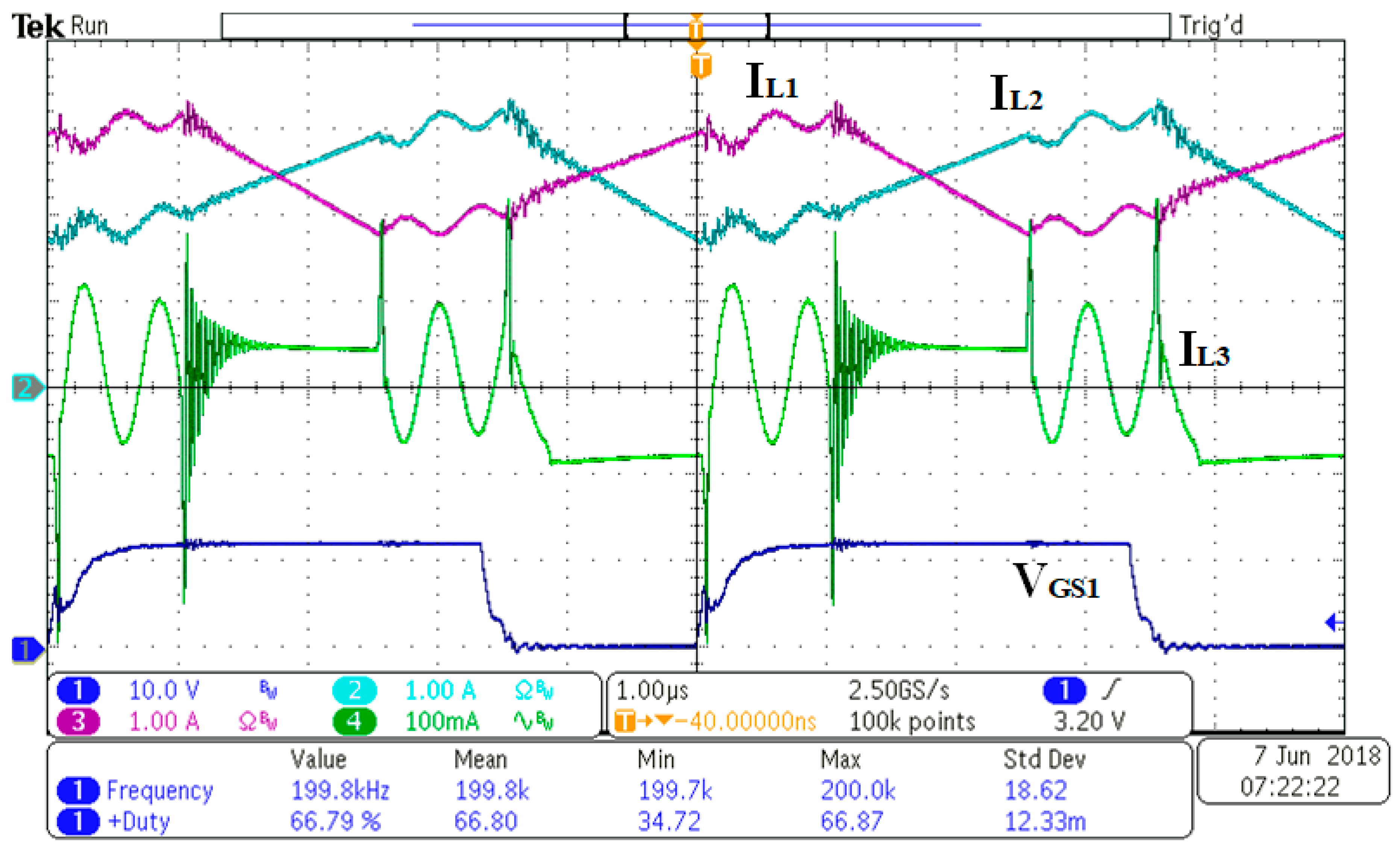
3.2. Measurement Results for D > 50% (65%)

Similar verifications as those from Figure 14 and Figure 15 were done for duty cycle value above 50% (Figure 16 and Figure 17). Figure 16 shows the current waveforms of the inductances together with one of the transistor´s gate drive signal. It is seen that compared to waveforms from Figure 14, the shape is more distorted mostly for the current L3. Amplitudes for the variables on L1 and L2 are the same and the only change for this operating condition is the change of the output voltage value (Figure 18) and the change of the AC current flowing through L3, which exhibits much more distortion and lower values.
Efficiency performance investigation was done for three operating conditions, which have been defined by the value of the operational duty cycle, whereby dependency on the output power delivery was evaluated. From Figure 18 is seen that the converter exhibits efficiency between 94.5% and 96.7% within 20% up to 100% of output power considering selected values of the duty cycle. From Figure 18 is seen that more efficient operation is for the duty cycle D = 50%, while whole operation region of the output power is considered, i.e. from 20% to 100% of nominal POUT. Efficiency decrease for the highest selected value of duty cycle (D = 65%) is caused by the distorted operation (Figure 16), by higher conduction losses in the main circuit due influence of the L3 inductance, and by the higher voltage difference between input–output part of the converter.
On the other side, it can be seen, that output voltage is able to increase directly with the increase of the duty cycle value (Figure 19) or by the change of the ration between inductances L1, L2, and L3, while ration between L1 and L2 is always considered to be 1:1.
Figure 20 shows the dependency of the voltage gain for investigated values of the duty cycle, while the dependency is evaluated on the turns ration change between the L1, L2, and L3, while as was already mentioned, the ratio between L1 and L2 shall always be 1:1 if the proper operation is expected. The ratio range is selected for the values, a which the operational waveforms of the currents and voltages are on the acceptable level considering efficiency performance.
Figure 21 shows the experimental evaluation of the influence of the input voltage variance on the efficiency for the operational condition when the output power is at its maximum, and duty cycle is at the worst selected condition (65%) from Figure 17. It is seen, that the input voltage variance has direct impact on the efficiency while considering the difference of 40 V at the input voltage causes 1.2% efficiency fluctuation.

3.3. Performance Comparisons to Other Topologies

For the performance analysis of presented converter to commercially used alternatives was realized in the way experimental measurements, while the proposed converter is compared to the standard dual-interleaved boost (DIB) type converter and to the classic boost converter [43]. The parameters of converters related to the output power, input voltage and switching frequency have been the same. It means each of converter operates at the maximum power of 500 W, at input voltage 100 VDC, with switching frequency 200 kHz. The voltage gain of all converters was set to the same level, i.e. Gain = 3.6. The results from the analysis related to the operational parameters/characteristics are listed in next table.
Table 4 shows that the proposed converter has the best efficiency from the investigated alternatives and it is also even the number of semiconductor switches is doubled oppose to standard alternatives. It is related to the type of magnetic component being used while the proposed converter uses much lower magnetic core and utilizes reset winding that is eliminating saturation of the core oppose to compared solutions. Due to very low output voltage ripple, the output electrolytic capacitors can be reduced, i.e. their value shall be much lower compared to standard topologies. In this way, the optimization is done also in the way of reduction of ESR and, thus, of other parts of losses. This is second issue related to the efficiency improvements of proposed converters. The proposed magnetic design of inductor is beneficial also due to fact, that it operates as stiff voltage transformer with the given transformer ratio. Existence of the visible AC component within the circuit secures, that the input current ripple is minimized. The only visible disadvantage of proposed converter to investigated one is the limitation of the voltage gain. With given turns ratio of inductor, it can achieve maximum value of 4. Anyway, if the ratio is modified, also higher values can be reached, but the performance of other variables can be then reduced [43].
A more comprehensive comparison can be done within future works, where the focus will be given also on the investigation of the semiconductor used and variant solutions of the main circuit with the possibility of resonant switching.

4. Conclusions

In this paper, the dual interleaved converter with coupled inductors and additional flux reset circuit was introduced and investigated. Principally the interleaved topologies offer several advantages to standard solutions, while mostly performance related to the lowered values of the output voltage ripple, and input current ripple are improved. Also, the efficiency is optimized through the wide operational range of input–output variances. However, there are still design considerations which negatively influence characteristics of the interleaved solutions. Since the boost coils work with DC magnetization, the demagnetizing circuit was introduced and investigated within presented paper. Such approach adds alternating current flow during each interval, thus AC part for the ferrite core is considered in this way. The main outcome is the reduction of the core direct saturation, so the better thermal performance and optimization of the geometrical properties is possible.
Because the analysis of the circuit was performed, several dependencies have been presented. The focus was given on the voltage gain characteristic dependent on the duty cycle change as well as on the turns ratio between boost and demagnetizing inductors. Both techniques were tested experimentally within the selected operational range on the prototype sample. Simultaneously the efficiency was estimated for various operational conditions, mostly for the variable output load at a constant duty cycle, while 3 scenarios were selected. Together with it the output voltage stiffness was also evaluated. The results showed that the most efficient operation is limited for the value of the duty cycle of 50%. On the other side, with low turns ratio between inductances, higher voltage gain is achieved above the 50% value of duty cycle.
Based on these considerations it is concluded, that proposed converter is possible to design for target application area with satisfying parameters from efficiency and voltage gain point of view. The designer just needs to decide, whether use duty cycle modification or turns ratio will be more effective. However, it is expected that the proposed converter topology can achieve 96% of efficiency within the whole operation range even when standard semiconductor devices are being used. A further increase is possible with wide bandgap devices.

Author Contributions

M.F. prepared the paper structure and has organized individual works within the paper preparations, made simulation analysis and finally he wrote the paper. B.H. has designed experimental prototype of proposed converter and has organized initial measurements. M.P. is responsible for the mathematical analysis. J.M. was realizing the experimental verification and analysis of the data from simulations as well as from experimental measurements.

Acknowledgments

The authors would like to thank for the support to the Slovak National Grant Agency APVV for project APVV-0396-15, to Slovak National Grant Agency VEGA for project Vega-1/0479/17 and to BH Motorsport company for support materials.

Conflicts of Interest

The authors declare no conflict of interest.

References

  1. Forouzesh, M.; Siwakoti, Y.P.; Gorji, S.A.; Blaabjerg, F.; Lehman, B. Step-up DC-DC converters: A comprehensive review of voltage-boosting techniques, topologies, and applications. IEEE Trans. Power Electron. 2017, 32, 9143–9178. [Google Scholar] [CrossRef]
  2. Ovcarcik, R.; Spanik, P.; Pavlanin, R. DC/DC converters used for a high input voltage based on a half-bridge topology. In Proceedings of the 6-th European Conference of TRANSCOM: 6-th European Conference of Young Research and Science Workers in Transport and Telecommunications, Žilina, Slovakia, 27–29 June 2005; pp. 57–62. [Google Scholar]
  3. Radika, P. High-efficiency DC-DC boost converter with passive regenerative snubber. J. Electr. Eng. Technol. 2014, 9, 501–507. [Google Scholar] [CrossRef]
  4. Perdulak, J.; Kovac, D.; Kovacova, I.; Ocilka, M.; Gladyr, A.; Mamchur, D.; Zachepa, I.; Vince, T.; Molnar, J. Effective utilization of photovoltaic energy using multiphase boost converter in compare with single phase boost converter. Commun. Sci. let. Univ. Zilina 2013, 15, 32–38. [Google Scholar]
  5. Dawidziuk, J. Review and comparison of high-efficiency high power boost DC/DC converters for photovoltaic applications. Bull. Pol. Acad. Sci. Tech. Sci. 2011, 59, 499–506. [Google Scholar] [CrossRef]
  6. Kim, D.-Y.; Won, I.-K.; Lee, J.-H.; Won, C.-Y. Efficiency Improvement of Synchronous Boost Converter with Dead Time Control for Fuel Cell-Battery Hybrid System. J. Electr. Eng. Technol. 2017, 12, 1891–1901. [Google Scholar]
  7. De Caro, S.; Testa, A.; Triolo, D.; Cacciato, M.; Consoli, A. Low input current ripple converters for fuel cell power units. In Proceedings of the 2005 European Conference on Power Electronics and Applications, Dresden, Germany, 11–14 September 2005; pp. 1–10. [Google Scholar]
  8. Choe, G.-Y.; Kim, J.-S.; Kang, H.-S.; Lee, B.-K. An optimal design methodology of an interleaved boost converter for fuel cell applications. J. Electr. Eng. Technol. 2010, 5, 319–328. [Google Scholar] [CrossRef]
  9. Cacciato, M.; Consoli, A.; Attanasio, R.; Gennaro, F. Multi-stage converter for domestic generation systems based on fuel cells. In Proceedings of the 41st IAS Annual Meeting (IEEE Industry Applications Society), Tampa, FL, USA, 8–12 October 2006; pp. 230–235. [Google Scholar]
  10. Lai, C.-M.; Lin, Y.-C.; Lee, D. Study and implementation of a two-phase interleaved bidirectional dc/dc converter for vehicle and DC-microgrid systems. Energies 2015, 8, 9969–9991. [Google Scholar] [CrossRef]
  11. Kascak, S. Analysis of Bidirectional converter with coupled inductor for electric drive application. In 2016 International Conference on Mechatronics, Control and Automation Engineering; Atlantis Press: Paris, France, 2016; pp. 229–232. [Google Scholar]
  12. Pavlovsky, K.M.; Guidi, G.; Kawamura, A. Assessment of coupled and independent phase designs of interleaved multiphase buck/boost DC-DC converter for EV power train. IEEE Trans. Power Electron. 2014, 29, 2693–2704. [Google Scholar] [CrossRef]
  13. Lee, J.-H.; Jung, D.-Y.; Park, S.-H.; Lee, T.-K.; Kim, Y.-R.; Won, C.-Y. Battery charging system for PHEV and EV using single phase AC/DC PWM buck converter. J. Electr. Eng. Technol. 2012, 7, 736–744. [Google Scholar] [CrossRef]
  14. Ruii, R.; Po, H.; Xu, L. Thermal analysis of a boost DC/DC converter in FCV for water content estimation based on AC impedance. In Proceedings of the 2016 IEEE Transportation Electrification Conference and Expo, Asia—Pacific (ITEC), Busan, Korea, 1–4 June 2016. [Google Scholar]
  15. Detka, K.; Górecki, K.; Zarebski, J. Modeling single inductor DCDC converters with thermal phenomena in the inductor taken into account. IEEE Trans. Power Electron. 2016, 32, 7025–7033. [Google Scholar] [CrossRef]
  16. Vellvehi, M.; Jorda, X.; Godignon, P.; Ferrer, C.; Milla´n, J. Coupled electro-thermal simulation of a DC/DC converter. Microelectron. Reliab. 2007, 47, 2114–2121. [Google Scholar] [CrossRef]
  17. Vuletić, R.; Zeljković, S.; Garg, P.; Denais, A. DC/DC converter development by means of electrical/thermal Co-simulationFrom concept to control algorithm and test. In INFORMATIK 2017; Lecture Notes in Informatics (LNI); Gesellschaft für Informatik, Bonn: Bonn, Germany, 2017; p. 515. [Google Scholar]
  18. Frivaldsky, M.; Spanik, P.; Drgona, P.; Loncova, Z. Algorithms for indirect investigation of heat distribution in electronic systems. Int. J. Thermal Sci. 2017, 114, 15–34. [Google Scholar] [CrossRef]
  19. Kim, N.; Han, C. Thermal analysis and design of a 75-W hybrid-type DC–DC converter for space applications. Microelectron. Reliab. 2014, 54, 1555–1561. [Google Scholar] [CrossRef]
  20. Gao, C.; Liu, H.; Huang, J.; Diao, S. Steady-state thermal analysis and layout optimization of DC/DC converter. In Proceedings of the Prognostics and System Health Management Conference (PHM-2014 Hunan), Zhangiiaijie, China, 24–27 August 2014. [Google Scholar]
  21. You, B.-G.; Lee, B.-K.; Lee, S.-W.; Jeong, M.-C.; Kim, J.-R.; Jeong, I.-B. Improvement of the thermal flow with potting structured inductor for high power density in 40kW DC-DC converter. In Proceedings of the 2012 IEEE Vehicle Power and Propulsion Conference, Seoul, Korea, 9–12 October 2012. [Google Scholar]
  22. Zhang, J. Bidirectional DC-DC Power Converter Design Optimization, Modeling and Control. Ph.D. Thesis, Virginia Polytechnic Institute and State University, Blacksburg, VA, USA, 30 January 2008. [Google Scholar]
  23. Pan, L.; Zhang, C. An integrated multifunctional bidirectional AC/DC and DC/DC converter for electric vehicles applications. Energies 2016, 9, 493. [Google Scholar] [CrossRef]
  24. Bhajana, V.V.S.K.; Drabek, P. A novel ZCS non-isolated bidirectional buck-boost DC-DC converter for energy storage applications. In Proceedings of the 24th IEEE International Symposium on Industrial Electronics (ISIE), Buzios, Brazil, 3–5 June 2015; pp. 1224–1229. [Google Scholar]
  25. Rosas–Caro, J.C.; Mayo–Maldonado, J.C.; Salas–Cabrera, R.; Gonzalez–Rodriguez, A.; Salas–Cabrera, E.N.; Castillo–Ibarra, R. A family of DC–DC multiplier converters. Eng. Lett. 2011, 19, 57–67. [Google Scholar]
  26. Sundari, N.; Jeba, D.; Ramalakshmi, R.; Rajasekaran, R. A performance comparison of interleaved boost converter and conventional boost converter for renewable energy application. In Proceedings of the 2013 International Conference on Green High Performance Computing, Nagercoil, India, 14–15 March 2013; p. 6, ISBN 978-1-4673–2592-9. [Google Scholar]
  27. Somkun, S.; Sirisamphanwong, C.; Sukchai, S. A DSP–based interleaved boost DC-DC converter for fuel cell applications. Int. J. Hydrog. Energy 2015, 40, 6391–6404. [Google Scholar] [CrossRef]
  28. Wang, C. Investigation on Interleaved Boost Converters and Applications. Ph.D. Thesis, Virginia Polytechnic Institute and State University, Blacksburg, VA, USA, 21 July 2009. [Google Scholar]
  29. Slah, F.; Mansour, A.; Hajer, M.; Faouzi, B. Analysis, modeling and implementation of an interleaved boost DC-DC converter for fuel cell used in electric vehicle. Int. J. Hydrog. Energy 2017, 42, 28852–28864. [Google Scholar] [CrossRef]
  30. Lai, C.-M.; Pan, C.-T.; Cheng, M.-C. High-Efficiency Modular High Step-Up Interleaved Boost Converter for DC-Microgrid Applications. IEEE Trans. Ind. Appl. 2012, 48, 161–171. [Google Scholar] [CrossRef]
  31. Akca, H.; Ayaz, R.; Durusu, A. Lifetime analysis of semiconductor switch of MPPT for different photovoltaic technologies considering ambient conditions. Electric. Eng. 2018, 100, 1881–1889. [Google Scholar] [CrossRef]
  32. Li, W.; He, X. ZVT interleaved boost converters for high-efficiency, high step-up DC-DC conversion. IET Electr. Power Appl. 2007, 1, 284–290. [Google Scholar] [CrossRef]
  33. Hartnett, K.J.; Hayes, J.G.; Rylko, M.S.; Barry, B.J.; Masłoń, J.W. Comparison of 8-kW CCTT IM and discrete inductor interleaved boost converter for renewable energy applications. IEEE Trans. Ind. Appl. 2015, 51, 2455–2469. [Google Scholar] [CrossRef]
  34. Lee, J.P.; Cha, H.; Shin, D.; Lee, K.J.; Yoo, D.W.; Yoo, J.Y. Analysis and design of coupled inductors for two-phase interleaved DC-DC Converters. J. Power Electron. 2013, 13, 339–348. [Google Scholar] [CrossRef]
  35. Martinez, W.; Imaoka, I.; Itoh, Y.; Yamamoto, M.; Umetani, K. Analysis of coupled-inductor configuration for an interleaved high step-up converter. In Proceedings of the 9th International Conference on Power Electronics and ECCE Asia (ICPE-ECCE Asia), Seoul, Korea, 1–5 June 2015; pp. 2241–2248. [Google Scholar]
  36. Kascak, S.; Prazenica, M.; Jarabicova, M.; Paskala, M. Interleaved DC/DC boost converter with coupled inductors. Adv. Electr. Electr. Eng. 2018, 16, 147–154. [Google Scholar] [CrossRef]
  37. Shen, C.-L.; Chen, H.-Y.; Chiu, P.-C. Integrated three-voltage-booster DC-DC converter to achieve high voltage gain with leakage-energy recycling for PV or fuel-cell power systems. Energies 2015, 8, 9843–9859. [Google Scholar] [CrossRef]
  38. Tseng, K.-C.; Chen, C.-T.; Cheng, C.-A. A High–Efficiency High Step-Up Interleaved Converter with a Voltage Multiplier for Electric Vehicle Power Management Applications. J. Power Electron. 2016, 16, 414–424. [Google Scholar] [CrossRef]
  39. Baharlou, S.; Yazdani, M.R. A non-isolated high step-up DC/DC converter with low EMI and voltage stress for renewable energy applications. J. Electr. Eng. Technol. 2017, 12, 1187–1194. [Google Scholar] [CrossRef]
  40. Revathi, B.-S.; Mahalingam, P. Modular high-gain DC-DC converter for renewable energy microgrids. Electr. Eng. 2018, 100, 1913–1924. [Google Scholar] [CrossRef]
  41. Tomaszuk, A.; Krupa, A. High efficiency high step–up DC/DC convertersA review. Bull. Polish Acad. Sci. Tech. Sci. 2011, 59, 475–483. [Google Scholar] [CrossRef]
  42. Frivaldsky, M.; Hanko, B.; Prazenica, M.; Morgos, J. High gain boost interleaved converters with coupled inductors and with demagnetizing circuits. Energies 2018, 11, 130. [Google Scholar] [CrossRef]
  43. Henn, G.A.; Silva RN, A.L.; Praca, P.P.; Barreto, L.H.; Oliveira, D.S. Interleaved-boost converter with high voltage gain. IEEE Trans. Power Electron. 2010, 25, 2753–2761. [Google Scholar] [CrossRef]
Figure 1. An electrical schematic of the proposed converter.
Electronics 08 01049 g001
Figure 2. Physical sample of the coupled inductor with the demagnetizing coil (a) and its equivalent circuit (b).
Electronics 08 01049 g002
Figure 3. Gate drive impulses for converter operation when the duty cycle of the transistor is below 50%.
Electronics 08 01049 g003
Figure 4. Gate drive impulses for converter operation when the duty cycle of the transistor is above 50%.
Electronics 08 01049 g004
Figure 5. Working intervals of proposed converter, D < 50% (35%).
Electronics 08 01049 g005
Figure 6. Working intervals, Duty > 50% (65%).
Electronics 08 01049 g006
Figure 7. Equivalent circuit schematics of the converter during 1st operational interval.
Electronics 08 01049 g007
Figure 8. Equivalent circuit schematics of the converter during 2nd operational interval.
Electronics 08 01049 g008
Figure 9. Equivalent circuit schematics of the converter during 3rd operational interval.
Electronics 08 01049 g009
Figure 10. Equivalent circuit schematics of the converter during 4th operational interval.
Electronics 08 01049 g010
Figure 11. Coincident (a) and anti-coincident directions of the coil’s windings (b).
Electronics 08 01049 g011
Figure 12. Proposed converter prototype.
Electronics 08 01049 g012
Figure 13. Experimental set-up with measuring equipment.
Electronics 08 01049 g013
Figure 14. Time–waveforms of the inductors currents. D = 35% Vin = 100V in Pout = 500 W.
Electronics 08 01049 g014
Figure 15. Time–waveforms of the inductors voltages. D = 35% Vin = 100V in Pout = 500 W.
Electronics 08 01049 g015
Figure 16. Time–waveforms of the inductors currents. D = 65% Vin = 100 V in Pout = 500 W.
Electronics 08 01049 g016
Figure 17. Time–waveforms of the inductors voltages. D = 65% Vin = 100 V in Pout = 500 W.
Electronics 08 01049 g017
Figure 18. Efficiency and output voltage in dependence on the value of the duty cycle and output power.
Electronics 08 01049 g018
Figure 19. Voltage gain dependency on duty cycle and output power.
Electronics 08 01049 g019
Figure 20. Voltage gain dependency on duty cycle and turns ration between L1, L2, and L3, while L1 = L2.
Electronics 08 01049 g020
Figure 21. Efficiency performance in dependency on input voltage at POUT = 100% and D = 65%.
Electronics 08 01049 g021
Table 1. Inductance and DC resistance values of coils.
L1 [µH]L2 [µH]L3 [µH]
Inductance [µH]297298573
DC resistivity [mΩ]414380
Table 2. Value of mutual inductances between coils.
L12 [µH]L13 [µH]L23 [µH]
Positive config (a)73012061200
Negative config (b)409440438
Table 3. Table of inductance couplings coefficients between coils.
k12k13k23
0.270.460.46
Table 4. Comparisons of the proposed converter to other circuit alternatives.
Proposed ConverterDIB ConverterBoost Converter
Output power500 W500 W500 W
Output voltage ripple19 mV180 mV364 mV
Input ripple current4.4 A17 A14 A
Output capacitor66 uF470 uF470 uF
Inductor VolumesE 43 PLTE50/27/15ETD59
Efficiency Pout=100%96.7%91%90%
Maximum achievable voltage gain1:61:191:10

