1. Introduction
Telemetry can be defined as a wireless communication process, used to collect data from remote or not accessible points and to send the acquired stream to a collection center, a device usually defined as a data logger [
1]. Through the analysis of the received data, it is possible to study a specific system behavior, to interact with it, and to properly control its evolution. Many different fields involve telemetry applications. For example, the telemetry has been applied to aeronautical instrument development, system defense, and biomedical applications [
2,
3,
4]. This work is focused on the usage of telemetry in the automotive field (in particular motorsport), where many parameters are acquired from different sensors at the same time. This allows the engineers to keep track of power-train performance and handling parameters such as suspensions, displacement, tire temperature, and so on [
5,
6]. The term telemetry refers to the data radio-transmission to the pits for remote and real-time monitoring of the vehicle during the competition and during the tests. This information is of crucial importance for the racing teams, because their analysis allows one to evaluate the car performance and to address its development [
7]. Moreover, data acquired from a car can be further processed in order to develop realistic simulators for drivers training [
8]. Telemetry is implemented in many different auto racing competitions, such as Formula 1, World Endurance Championship (WEC), and World Turing Car Championship (WTCC) where the Wi-Fi technology is adopted as a data transmission medium. During the race, the telemetry data must be sent in real-time to the pits, therefore, it is necessary to guarantee a complete network coverage of the entire track. This coverage is typically realized through different Wi-Fi bridges, placed along the circuit path. Unfortunately, a complete network coverage cannot be guaranteed in all car racing competitions, moreover it is very complex and expensive. For instance, in rally races, it is difficult to install Wi-Fi bridges or other kinds of repeaters along the track. Thus, telemetry must be implemented in a different way. The data cannot be sent in real-time to the pits, but they must be stored in the data logger, mounted on the vehicle. Thus, the analysis of all the telemetry data can be done once the data logger is extracted from the car [
9].
The aim of this paper is to present a new data logging system for automotive applications which has been designed in collaboration with the motorsport department of Magneti Marelli Inc., a leader in the motorsport field. The system is composed of an electronic board that will be permanently installed in the car, and by a removable device which stores all the sensor data transmitted by the other part of the system. A resonant inductive coupling circuit powers the whole system and, for this reason, the distance between the two parts of the system must be kept small.
The communication procedure is based on a visible light communication (VLC) technology. The choice of this technology strongly depends on the presence of electromagnetic interference in the car, which can affect the performance of other technologies such as radio-frequency identification (RFID) and near field communication (NFC). Moreover, VLC ensures a higher throughput than RFID and NFC.
Several different solutions are commercially available, such as the SLD system [
10] produced by Magneti Marelli Motorsport or DA3 [
11] produced by GEMS. However, new necessities, concerning the high data-rate required and the structure of the device, together with limits on the power consumption, prevent one from using the existing components.
The proposed system reaches a throughput of 21 Mbit/s with a power consumption of 0.5 W, which outperforms most of the commercial solutions on the market. Moreover, our work exploits VLC, while the commercial products are typically based on different kinds of wired busses. Therefore, our system is more reliable than the other commercial solutions, since it is less prone to the electromagnetic noise. It is worth noting that the adopted technologies are well-established, which is an added value because the developed system must be reliable and well supported on the market. The main contribution of this work is the integration of these technologies into a device which, to the best of authors’ knowledge, outperforms commercial-off-the-shelf (COTS) solutions.
The paper is organized as follows. First, the description of the new proposed system together with the process constraints are reported. Then in
Section 3, a detailed explanation of the adopted transceiver is provided. Moreover, the built test system and the developed test program are shown. Then, the system has been upgraded and a new proposed one is described in
Section 4, together with the tests performed in order to analyze the transceiver characteristics. Finally,
Section 4 shows how the new developed system satisfies all the process constraints and performs a comparison with the state-of-the-art solutions.
2. Materials and Methods
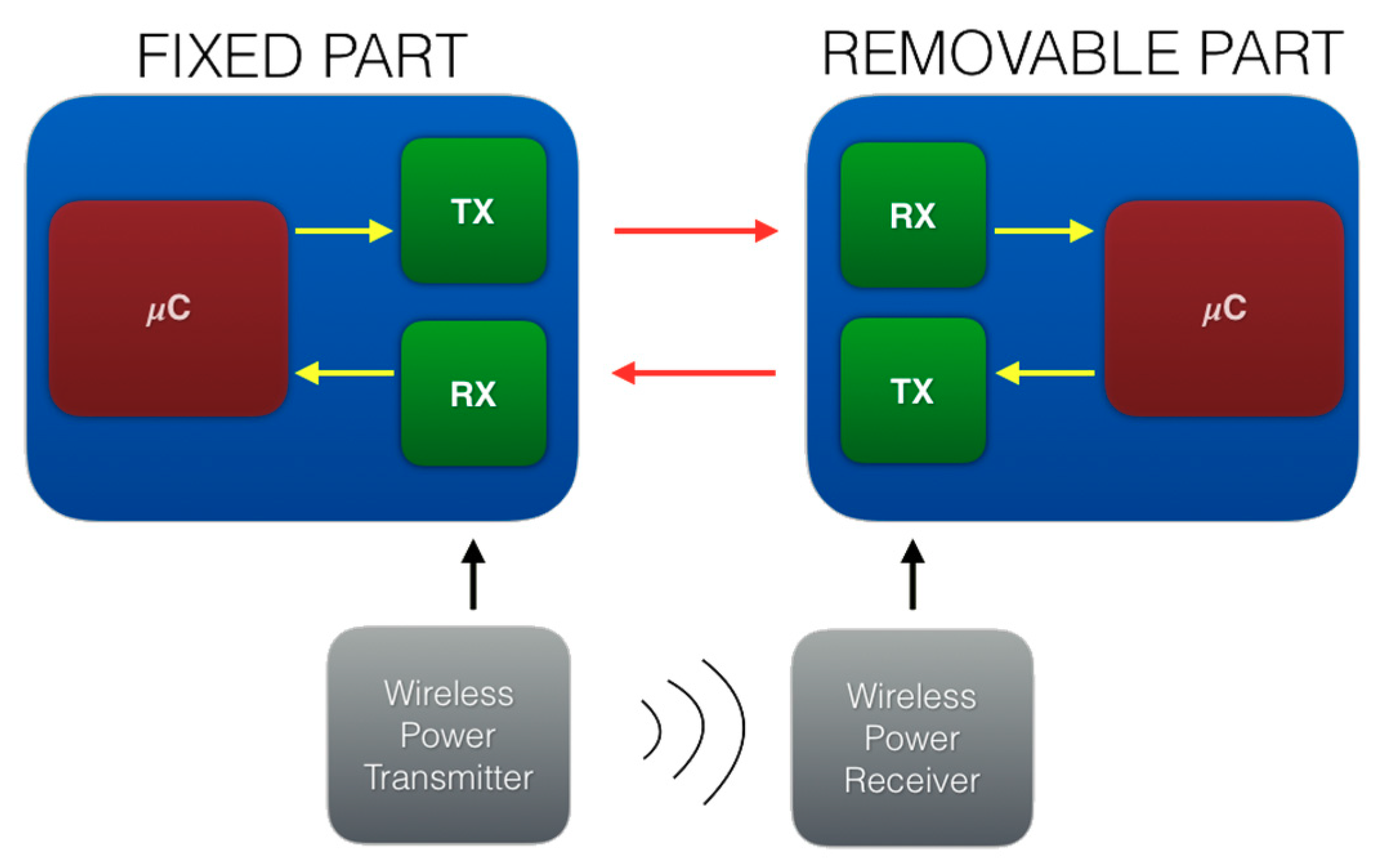
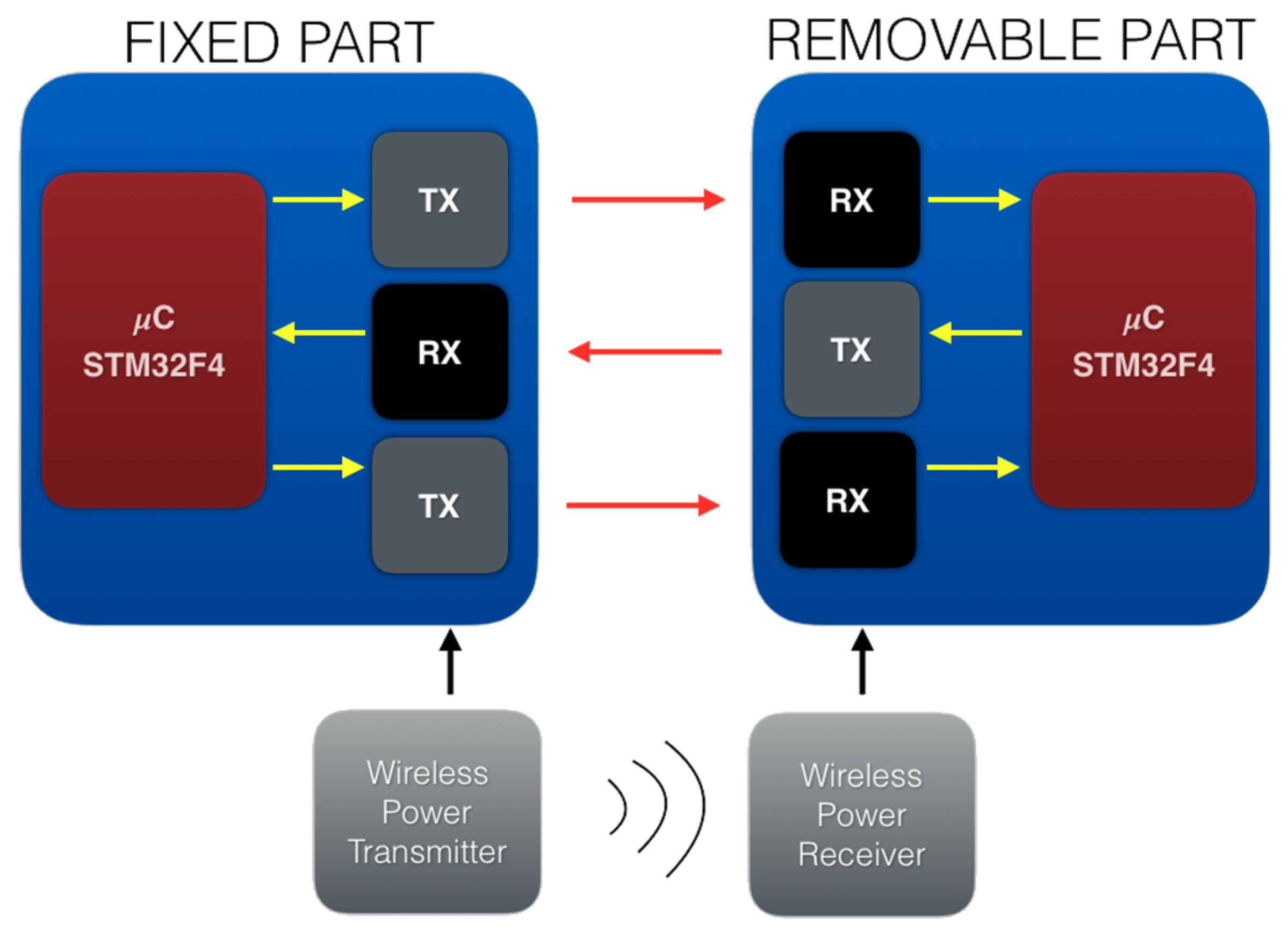
Figure 1 shows a block diagram of the proposed data logging system. The fixed part collects data coming from the car central unit via a wired Ethernet connection and transmits them to the removable part, which stores them in a flash memory.
TX and RX are two components, which are used to send and receive data, respectively. These two devices, considered together, constitute the transceiver, which is used to exchange data between the fixed and the removable parts of the system. A suitable transceiver data transmission medium has to be found in order to satisfy all the process constraints.
μC indicates the micro-controller which manages the exchange of messages by communicating with the transceiver through a suitable port which is based on a transistor-transistor logic (TTL). The transceiver also must be compliant with the TTL logic which defines the constraints through which a signal is identified as high or low by the port. A TTL input signal is considered low when it is within 0 V to 0.8 V, while it is identified as high when it goes from 2.2 V up to 5 V and, in this way, the port distinguishes the two logic levels 0 and 1, respectively. The fixed part acquires data through the Ethernet connection and sends them immediately through the transceiver to the removable part, which stores them in a flash memory.
Once the removable device is extracted, all the information acquired can be downloaded on a PC via USB.
Many data loggers are present on the market, but, to the best of the authors’ knowledge, no one of them is composed by a fixed and a removable part which can be quickly extracted, can guarantee a data rate of at least 8 Mbit/s and can work in a very noisy environment.
In order to develop the entire system reported in
Figure 1, it has been decided to use the STM32F3DISCOVERY [
12] board (STMicroelectronics, Geneva, Switzerland) and its micro-controller. It is characterized by an ARM Cortex-M4 (Atmel, San Jose, CA, USA) 32-bit CPU equipped with a floating point unit (FPU) working at a maximum frequency of 72 MHz. It is also equipped with 256 KB of Flash memory and 48 KB of static RAM (SRAM). The board can be powered through an USB bus or from an external 3 V or 5 V voltage generator. The USB interface is also used for debugging and programming.
Specifically, we chose to connect the transceiver to the universal asynchronous receiver-transmitter (UART) port of the micro-controller.
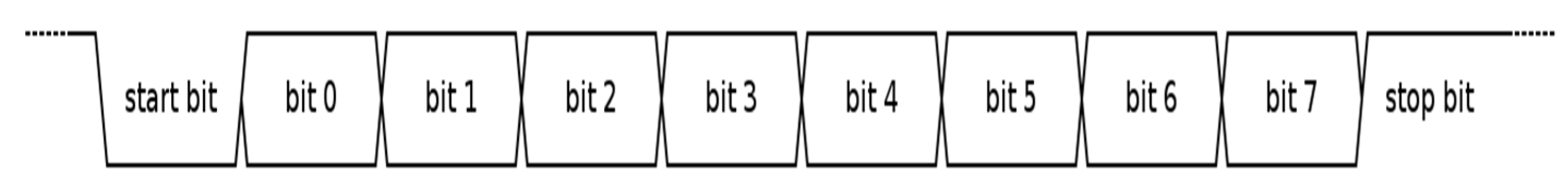
In
Figure 2, an example of an UART data format is reported. Since the communication is asynchronous, the receiver has to sample the communication line in order to find the start bit. The subsequent bits, whose number can be changed, represent the real data. At the end of the packet, a stop bit is inserted.
Inside the STM32F3DISCOVERY board, five UART ports are available. Each port has a programmable data word length (7, 8 or 9 bits) and stop bits (1 or 2 stop bits). Moreover, the UART ports can use the direct memory access (DMA) engine which allows a continuous communication by providing high speed data transfer between the memory and the peripheral and vice versa without any CPU actions.
3. System Architecture
3.1. The Proposed System
In order to provide a solution with a better data rate and lower power consumption than in other COTS solutions, and to also overcome the limitations due to the absence of Wi-Fi bridges, the new datalogging system must fulfil the following requirements: the data coming from the car central unit must be stored in a removable device that can be inserted and extracted as fast as possible, when needed. The system should also be reliable even in a very noisy environment. The constraint on transmission speed is that the throughput must be greater than 8 Mbit/s. Finally, the power consumption must be kept contained, below 2 W.
An accurate study has been conducted in order to find the proper technology for the transceiver data transmission medium. In this analysis, not only must the process constraints be taken into account, but also the transceiver availability in the market and its compatibility with the micro-controller port.
Technologies such as USB or Ethernet, which need an electrical connection between the two parts of the system, have been rejected. Indeed, they can guarantee the required communication speed, but they do not allow a quick extraction/insertion of the removable device in a fast way, without causing damages on both devices. Several tests have been made to verify the possibility to implement a physical connection between the fixed and the removable part, but the results were not satisfactory even using a military USB connector. Thus, a wireless communication system has to be designed.
Concerning the choice of the data transmission medium, many disturbances, which prevent the correct data transmission, must be considered. Usually, they are in the frequency range up to 100 GHz and are due to the presence of different devices which must be installed on the racing vehicles. For this reason, solutions based on Wi-Fi and Bluetooth, have been rejected and it has been decided to adopt a transmission medium which works at higher frequencies: visible light. This technology has been adopted in many different applications, but only recently has it obtained great success as a data transmission medium. An example is represented by Li-Fi [
13,
14,
15], a new technology which uses the light emitted from an LED as a data transmission medium implementing the so-called visible light communication (VLC). The Li-Fi works in a similar way as the Wi-Fi, but it can guarantee higher speeds, it requires fewer components than radio technology and it avoids the use of radio frequencies, which may interfere with electronic circuit. Moreover, the Wi-Fi adopts the radio waves as the data transmission medium and the radio frequency spectrum is reaching its full capacity while the visible light spectrum is 10,000 larger than the previous one [
16]. On the other hand, Li-Fi has some drawbacks, such as the need for a clear line of light. However, these requirements do not prevent the use of Li-Fi technology inside the considered process.
3.2. The Choice of the Transceiver
In order to find the proper device which could be used as the transceiver inside the system, a detailed search on the market has been carried out. At the end, two components, produced by Broadcom Company, have been discovered: AFRB-1634Z and AFBR-2634Z [
17]. They are a link fiber optic transmitter and receiver, respectively, which are designed to work with 1-mm polymer optical fiber (POF). However, by keeping a short distance between the two devices, they can work even without cables. In this way, any physical connection is avoided. The transmitter (AFBR-1634Z) is composed of a 650-nm LED and a driver integrated circuit with TTL input logic. The receiver (AFBR-2634Z) consists of a photodiode and a digitalizing integrated circuit with TTL output logic. Moreover, their operating temperature ranges from −40 °C to 85 °C, which is the typical requirements wanted for motorsport devices. They can be powered by 3.3 V or 5 V requiring a maximum supply current of 31 mA and 30 mA for the transmitter and receiver, respectively. This means that, in the worst case, the total power consumption is equal to 305 mW.
These two components have a package which allows to easy connection between one device and the other. In this way, a compact transceiver carried out and it can support a data rate up to 50 MBaud. Thus, with AFBR-1634Z and AFBR-2634Z components it is possible to build a transceiver which can satisfy the process constraints concerning the data rate and the absence of physical connection. Furthermore, the transmitter adopts the visible light as data transmission medium and so even a high noise rejection is achieved.
Concerning the transmission data technique, it has been decided to adopt an on-off keying (OOK) modulation which is the simplest form of the amplitude-shift keying (ASK) modulation. It represents the digital data with presence or absence of a carrier wave. This means that a logic 1 will be coded by turning on the LED, while for a logic 0 the LED remains off.
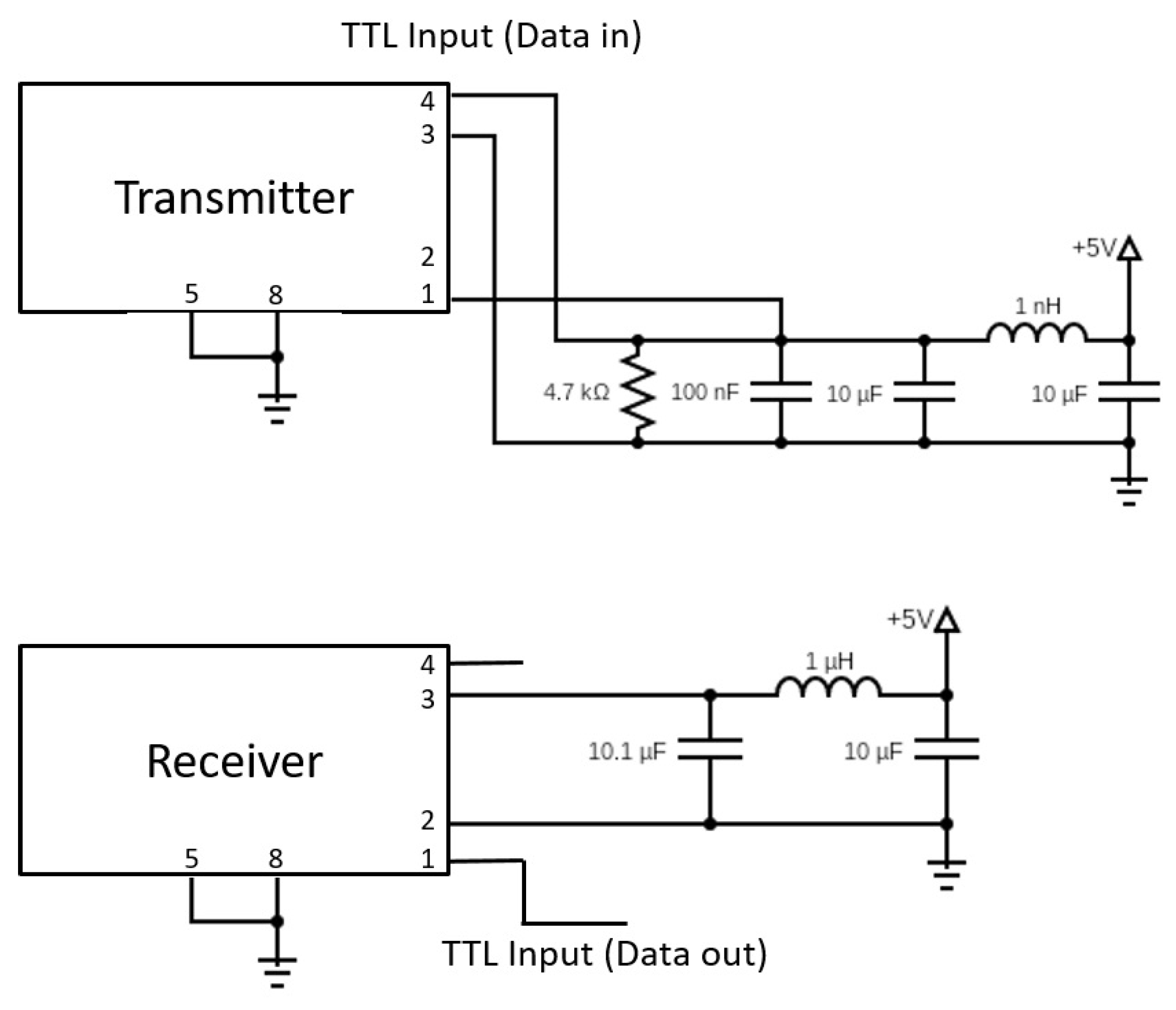
As shown in
Figure 3, the transceiver has a basic application circuit which is built with one inductance and several capacitors. These components are used to filter the power supply (VCC) which can be 3.3 V or 5 V.
Since the input and output pins are compliant with the TTL logic, they can be directly connected to the port of the micro-controller without any external electronic, except a pull-down resistor on the transmitter pin.
Concerning the TTL input pin, by applying a voltage below 0.8 V or greater than 2 V, the LED will be turned off or on, respectively. On the other hand, the TTL output pin will produce an output voltage of at most 0.8 V or VCC which represents logic 0 or 1, respectively. Since the value of the power supply can vary, it is necessary to carefully connect the transceiver to the micro-controller. Indeed, it will be necessary to use micro-controller pins which tolerate the chosen VCC value in order to avoid any damages.
4. Results and Discussion
In order to test the two Broadcom components, it has been decided to apply on the transmitter input pin a voltage square wave generated through a pulse wave generator. The receiver output pin has been connected to an oscilloscope in order to analyze the generated signal.
In
Figure 4, the purple signal is a 1 KHz square wave between 0 V and 3.3 V applied on the transmitter input pin while the yellow one is the receiver output signal. It is important to notice that both the signals are equal, i.e., the information has been correctly sent and received. Moreover, the receiver output signal has voltage values that range from 0 V to 5 V. This is due to the fact that the component has been connected to a power supply of 5 V.
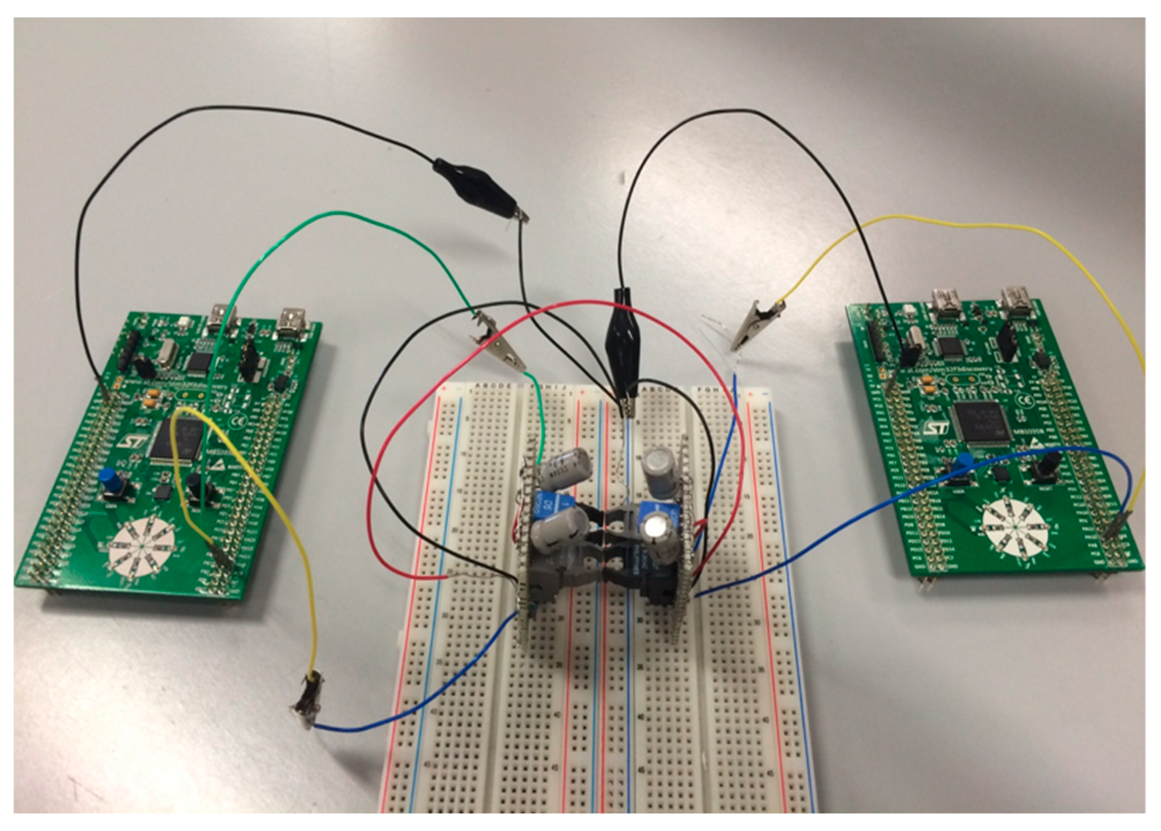
After having validated the transceiver, a test system (
Figure 5) has been developed. In this case, the two boards have been powered through the PC USB port while the transceiver through a power supply. Among the five UART ports of the micro-controller, we decided to use the UART1 since it is the only one which can guarantee a data rate of 8 Mbit/s with a CPU clock frequency of 72 MHz.
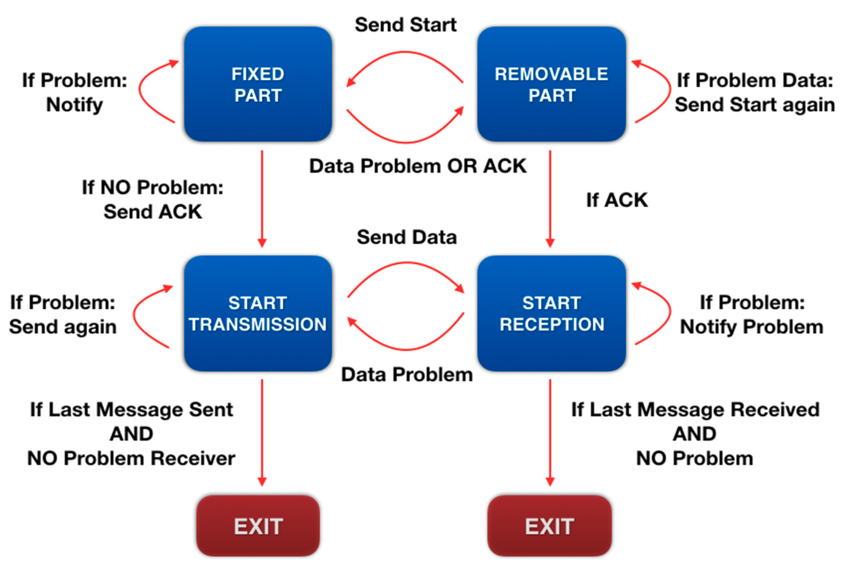
A test program, whose block diagram is reported in
Figure 6, has been implemented. The communication starts with a handshake phase between the two parts of the system. The removable part notifies its presence and its data request to the other part of the system through a “Send start” message.
If the fixed part correctly acquires the request, it answers with an “ACK” message, otherwise it notifies an inconvenient through a “Problem data” message. In this case, the removable part has to dispatch again the “Send start” message.
If there are no problems during the handshake phase, the fixed part starts the transmission of all the data, which are stored by the removable part inside its memory. The removable part sends a “Problem data” message only in the case of a problem inside the received data. These kinds of problems, such as frame errors, noise errors, or overrun errors, prevent one from correctly understanding the received data. Therefore, a data retransmission is necessary, however, this reduces the system performance.
Finally, when the last message has been sent without problems, the program on both the micro-controllers exits.
Through this test, the quality of the data transmitted has been verified since no retransmission has been required.
4.1. System Upgrade
As reported in the transceiver datasheet, the maximum allowed data rate is 50 Mbit/s. This means that the transmission speed of 8 Mbit/s inside the proposed system is due to the micro-controller limits. Indeed, using an asynchronous communication protocol, the maximum data rate depends on the sampling frequency of the micro-controller port. Thus, it has been decided to upgrade the micro-controller by using the STM32F4DISCOVERY board [
18]. It is equipped with an ARM Cortex M4 32-bit CPU with FPU working at 168 MHz, 1 MB of Flash memory, and 192 KB of RAM. The board can be powered through the USB bus or from an external 3 V or 5 V voltage generator. The USB interface is used for debugging and programming.
Concerning the previous micro-controller, the memories have been expanded and the clock frequency has been increased. As said before, the clock frequency influences the maximum achievable data rate through the UART ports and it has been increased from 72 MHz to 168 MHz. Even if the clock speed is more than double that of the previous micro-controller, the UART port is connected to a domain which can provide a maximum clock frequency of 84 MHz. This means that the maximum data rate achievable is only equal to 10.5 Mbit/s not much greater than before. Thus, in the STM32F4DISCOVERY board the micro-controller can work at a very high speed greater than the double of the speed of the previous board, but the UART port does not present the same performance.
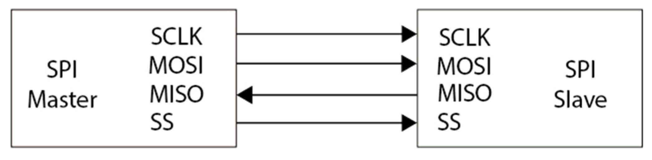
As shown before, the UART communication speed is limited by the sampling frequency of the port. This is a typical characteristic of the asynchronous communication protocol. Indeed, the receiver must continuously sample the line in order to find the start bit of the message. Thus, it has been decided to adopt a different transmission strategy by using the synchronous serial peripheral interface (SPI) communication protocol. The SPI layout is shown in
Figure 7 where SCLK is the serial clock, MOSI is the master output slave input, MISO is the master input slave output, and SS is the slave select.
This protocol is based on the presence of a master which can communicate with different slaves. Since the exchange of messages is synchronous, the master has to share the clock on the SCLK line with one of its slaves, which will be selected through the SS link. The master sends and receives data to and from the slave on the MOSI and MISO lines, respectively. All the parts involved in the communication have to agree on the procedure adopted to read and write each single bit of the message. It has been decided to write and read on the rising and falling edge of the clock, respectively.
Even the SPI port, as the UART one, has an internal shift register which converts data from a parallel to a serial way and vice versa and can be accessed through the DMA allowing a high-speed communication between peripheral and memory.
In order to realize an SPI communication between the two parts of the system (
Figure 1), it is necessary to add another LED and photodiode, as shown in
Figure 8, on the fixed and removable parts of the system, respectively. This new couple LED-photodiode will be used to wirelessly share the clock between the master (fixed part) and the slave (removable part).
By passing from an asynchronous to a synchronous communication procedure, it is possible to increase the transmission data rate up to 21 Mbit/s. However, this limit is not given by the micro-controller, as it happened before with the UART port, but by the transceiver maximum data rate (50 Mbit/s). Indeed, the SPI port supports a data rate up to 42 Mbit/s but the shared clock has a frequency which is double that of the data rate. This means that it cannot be sent through the Broadcom components. For this reason, it is necessary to reduce the data rate to 21 Mbit/s so that the clock can be shared correctly between the master and the slave. In the STM32F4DISCOVERY board, starting from the maximum allowed data rate of 42 Mbit/s, it is possible to divide this value only by powers of 2. Thus, the closest value supported by the proposed system is 21 Mbit/s.
By adding other electrical components, the data rate has been doubled compared to the previous solution, but the power consumption has been increased from 305 mW to 455 mW. However, even with this small increase, the total power consumption remains far below 2 W, which is the considered process constraint. Still, 1.5 W remains in order to power the micro-controller.
As it was done before, a new test system and its relative program have been developed. In this test, all the components of the removable part have been powered through the inductive coupling circuit. Due to the micro-controller memory limits, a total of 60 KB of data have been continuously sent from the master to the slave and they have been correctly received without any source of problems. Both the transmission and the reception has been managed through the DMA which, in the master board, has to take the data value from the RAM memory and transfer it to the SPI port while, in the slave, it has to do the opposite procedure. In order to analyze the received data, it is possible to connect the board to the PC through a USB cable. However, this connection also provides the power supply to the board which avoids testing the inductive coupling circuit of the test system. For this reason, after having completed the reception, the slave must store all the data received inside the flash memory mounted on the board. In this way, even if the board is turned off, the data will permanent be available. Thus, only after having completed the communication procedure, the slave board will be connected to the PC and the data received will be downloaded. In this way, it is possible to test the correctness of the result by comparing the sent and received data.
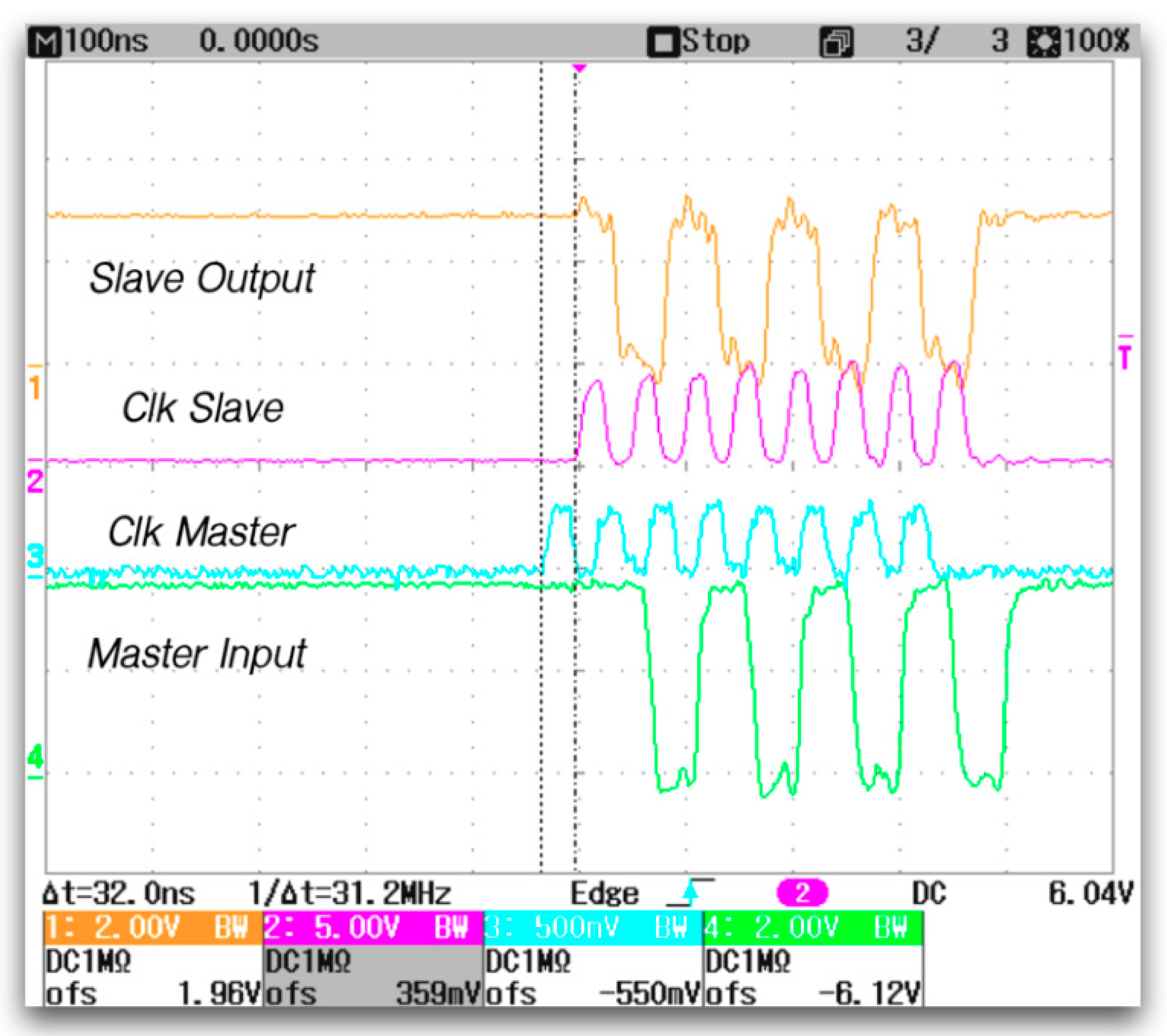
The choice of a synchronous communication technique, as the SPI one, allows it to reach a data rate of 21 Mbit/s increasing the total power consumption only by a few Watts. However, there is a drawback in the adopted solution which can be noticed in
Figure 9. By analyzing the purple signal, which represents the clock received by the slave, it is possible to observe a delay of 32 ns compared to the blue signal (the clock sent by the master). Moreover, the same delay is present between the signal sent by the slave and received by the master. As said before, the SPI port has been configured in order to read and write each single bit on the rising and falling edge of the clock, respectively. Thus, considering the blue and the green signals, it is possible to notice that the rising edge of the clock is aligned with the transition of the master input signal avoiding a correct reading of the input signal. This means that the slave is not able to send complex messages to the master, but it can only use 1 or 0 in order to notify the correctness of the received data. However, this limit does not have a big impact on the process since all the data are sent from the master to the slave which only has to notify if there were a problem in the received data.
If the slave had to exchange a more complex message, different solutions could be explored. First, the master could reduce the data rate only when it wants to receive data from the slave. In this case, the small delay of 32 ns can be ignored. Another solution concerns the insertion of another LED and photodiode on the slave and master board, respectively. In this way, the total power consumption increases, but the slave, once it has to send messages, can temporarily become the master of the communication.
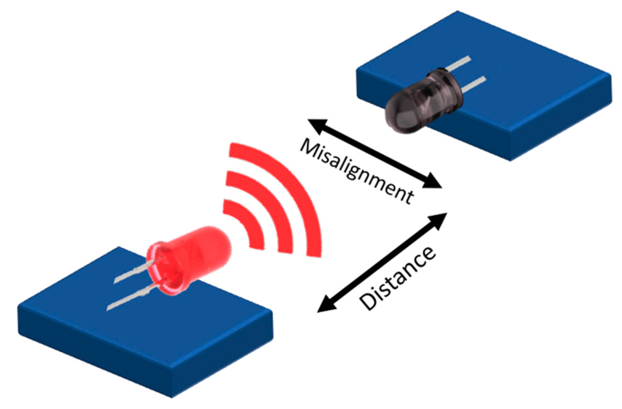
4.2. Distance and Misalignment Tests
As shown in
Figure 10, two last experiments have been performed: the distance and misalignment tests. The former concerns the evaluation of the maximum distance at which the AFBR-1634Z and AFBR-1624Z components can work even without an optical fiber connection while the latter evaluates the maximum misalignment between the LED and photodiode.
The distance test results are shown in
Table 1. In the first column, the distance has been reported between the LED and photodiode. The first value considered is 2.3 cm and this is due to the components package where this is the lowest allowed size. The “Light Received” column indicates the photodiode capability of perceiving the light emitted by the LED while the “Data Received” one represents the slave capability of correctly receiving 60 KB from the master. As shown in
Table 1, it is possible to obtain a correct data transmission of up to 2.6 cm. At a distance of 2.9 cm, some problems start to appear. Even if the photodiode can reveal the light emitted by the LED, the data cannot be correctly received. This is due to the LED emitting power, which hits the photodiode surface and is not sufficiently high to produce a current to be converted in a high voltage level. This means that the photodiode cannot reproduce a signal transmitted by the LED which has continuous transitions from low to high and vice versa at high frequencies. However, if the photodiode surface is hit by the LED light for enough time, it will generate a high voltage value. Finally, at 3.2 cm, not only the data but also the light cannot be received correctly by the photodiode.
The last test has been carried out in order to verify the behavior of the system after a misalignment. The LED has been fixed while the photodiode has been placed at different distances and it has been shifted with a step of 0.02 mm. At each step, the correct operativity of the system has been verified. The test results are reported in
Table 2.
The experiments pointed out that the LED and photodiode should be kept aligned as much as possible. Honestly, only a small misalignment is allowed by its value decreases by increasing the distance. This phenomenon is due to the fact that the optical power, hitting the photodiode surface, decreases when increasing the distance. For this reason, the LED and photodiode should be kept more aligned in order to correctly receive the signal.
All of these tests have been performed by keeping the two Broadcom components inside their packages which are designed to work with optical fibers (i.e., reduce its emission angle and focus the light inside the fiber). However, this characteristic is not required in the proposed work since no optical fiber has been used. This means that it is possible to directly use the LED and photodiode present inside the two packages. In this way, it is possible to reduce the distance between the LED and photodiode as well as the maximum misalignment allowed.
4.3. Discussion
The choice of adopting VLC technology has been conceived on the basis of the data volume to transfer and to the possible presence of electromagnetic noise. Concerning the channel limitations of the VLC, they are related to the ambient light interference and the line-of-sight propagation. The ambient light interferes with the communication if and only if this light is stronger than the light used for communicating. In the proposed solution, this is not a critical issue, since the communication process is constrained inside a much protected environment. On the other hand, the light-of-sight propagation issue has been addressed in the paper, by evaluating the maximum allowed distance and misalignment with the adopted transceivers. Again, the case which contains the removable part of the system has been designed to respect these ties. Therefore, the main limits of VLC are overcame by the design solutions.
About the data volume, one of the described process constraints is that the throughput should be greater than 8 Mbit/s, since the system should be capable of handling different data type transmission. In modern motorsport competitions, data is acquired from different kind of sensors, including image sensors. The data volume to transfer is always increasing, therefore, the choice of VLC technology is the most suitable one (looking even to future applications), since it has a larger bandwidth than RF communication.
The maximum data rate allowed is 50 Mbit/s which is much greater than the 8 Mbit/s, defined by the Magneti Marelli Company constraints. The communication procedure is managed by a micro-controller mounted on each of the two parts of the system. All of the system is powered by an inductive coupling circuit. The first solution foresees the use of the STM32F3DISCOVERY micro-controller and a UART port in order to develop an asynchronous communication between the fixed and the removable part of the system. In this case, the maximum data rate achievable is equal to 8 Mbit/s. After that, it had been decided to change the micro-controller with the STM32F4DISCOVERY one, which is more performant. However, the maximum data rate achievable is 10.5 Mbit/s, which is only few greater than the value obtained through the previous solution. This brought us to conceive a new solution passing from an asynchronous to a synchronous communication procedure. It is implemented through the SPI port of the micro-controller allowing a data rate of 21 Mbit/s.
The power consumption is in every case below 0.5 W and so 1.5 W can be used to power the micro-controller since 2 W is the considered constraint requested by Marelli.
The proposed solution is compared with the COTS solutions described before and with the recent work of Fertitta et al. [
19] in
Table 3.
From
Table 3, it is possible to see that the proposed solution outperforms the COTS ones by providing a better data rate, together with a lower power consumption. The advantage in required power consumption is maintained also with respect to [
19], which consumes four-times more power. On the other hand, the solution designed in [
19] is capable of providing a higher data rate compared to our best solution. However, it is important to emphasize that our solution is the only one based on VLC, which does not require cables.

 ,
, 


