Abstract
In this paper, a comprehensive double-vector approach is proposed to alleviate the common-mode voltage of voltage-source inverters based on a model predictive control scheme. Only six active vectors are selected to alleviate the common-mode voltage. Furthermore, one sampling period must be split to apply two non-zero vectors, which can generate currents with small current ripples and errors, despite not using zero vectors. The developed algorithm regards in full all 36 possible cases combined by two non-zero active vectors when selecting two vectors and splitting them into one sampling period. Thus, an optimal future set of two non-zero active vectors and optimal durations of two non-zero active vectors to produce the smallest current errors between the real currents and the reference in future load current trajectories were selected from 36 entire sets. This was done to minimize the cost function defined at the time when it varies from the first vector to the second vector and at the next sampling instant. Thus, the proposed algorithm can control the output currents with a fast transient response and reduce output-current ripples and errors, as well as alleviate the common-mode voltage to .
1. Introduction
Three-phase voltage-source inverters (VSIs) have been used commonly to generate three-phase line currents, while the frequencies and amplitude of the three-phase line currents are changeable [1,2]. In VSIs, the fast switching operation results in common-mode (CM) voltage, which has been considered the cause of over voltage stress to surrounding electronic systems [3,4,5,6,7,8]. To alleviate the amplitude of the CM voltage, multifarious studies have been conducted with a PWM algorithm that is designed by only selecting the non-zero active vectors, and this is because the zero vectors produce the highest CM voltage [3,4,5,6,7,8]. However, when the inverter is controlled by only using the non-zero active vectors without selecting the zero vectors, the Total Harmonic Distortion (THD) and error of the output currents of the inverter inevitably deteriorate. This is because zero vectors typically produce the smallest variation in the load dynamics. Therefore, methods for reducing the CM voltage without deteriorating the inverter performance have been studied extensively [9,10,11,12,13,14,15,16]. Recently, a model predictive control (MPC) method was studied for VSIs owing to its flexibility and simplicity of control [17,18,19,20,21,22,23,24,25,26,27,28,29]. Utilizing the basic principle that VSIs can apply two zero vectors and six different non-zero active voltage vectors to the load, seven different future current behaviors, which change according to the voltage vectors, can be predicted by the MPC method. The possible future currents of the VSI can be calculated using the load dynamic model. Based on the cost function, which is predefined as the error between the reference currents and the predicted output currents, all predicted currents calculated by the seven different possible cases using the load dynamic model can be used to choose one voltage vector to minimize the predefined cost function. However, in the conventional MPC method which selects only one voltage vector during the sampling period, if only the active vector is used to reduce the CM voltage without using a zero vector which produces the highest CM voltage, the current error and current total harmonic distortion (THD) are inevitably higher than those of the method using PWM blocks. To overcome these problems, MPC methods using a double vector (DV) have been studied [8,17,18]. In this paper, there are two conventional DV-MPC algorithms, called DV-Conv1 and DV-Conv2. In the DV-Con1 method, two vectors closest to the reference are first selected, and then the sampling period is divided for minimizing the cost function [10]. In the DV-Con2 method, one vector closest to the reference vector is selected first, and the second vector is selected by dividing the sampling period to minimize the cost function [8,17,18]. However, such control methods have a disadvantage in that the calculation time is increased and if the conventional algorithm is operated with a half sampling period, selecting two vectors at one sampling period, for fair comparison, the current ripples and errors of the DV-Con1 and DV-Con2 methods are higher than those of the conventional method which selects one vector during one sampling period. Finally, the VSI using the MPC method applies the optimal voltage vector during each sampling period. Because of its simplicity, the MPC method has been used extensively to control the line current of many non-VSI converters, which are matrix converters, multiphase inverters, and multilevel inverters [19,20,21,22,23,24,25,26,27,28,29,30].
This paper proposes a comprehensive DV method to mitigate the CM voltage in VSIs based on the MPC scheme. Only six active vectors are utilized to control currents to alleviate the CM voltage in the proposed algorithm, because the zero vector makes the highest CM voltage. Therefore, the proposed algorithm can alleviate the CM voltage within except for the two zero vectors which make the CM voltage within . Furthermore, the proposed algorithm uses two non-zero active vectors at one sampling period to compensate for the decreased number of candidates. The proposed algorithm selects two non-zero active vectors and divides them within one sampling period by considering all 36 possible combinations produced by the six non-zero active vectors to minimize the predefined cost function. This optimization process can minimize current ripples and errors. The proposed algorithm makes small current ripples and errors compared with the conventional algorithm despite not using zero vectors. The proposed algorithm also has a better control performance compared with the DV-Con1 method and DV-Con2 method because the proposed algorithm considers more cases than the two methods. Furthermore, as a solution to the computation time delay, the delay compensation technique was used in the proposed algorithm. In addition, the zero vectors are not selected in the normal transient condition, therefore the proposed algorithm does not adversely affect the fast transient response. To verify the proposed algorithm, simulation and experiment were performed.
2. Conventional Model Predictive Current Control Method for VSIs
Figure 1 shows the three-phase VSI, where the voltage vector applied to the load can be denoted as
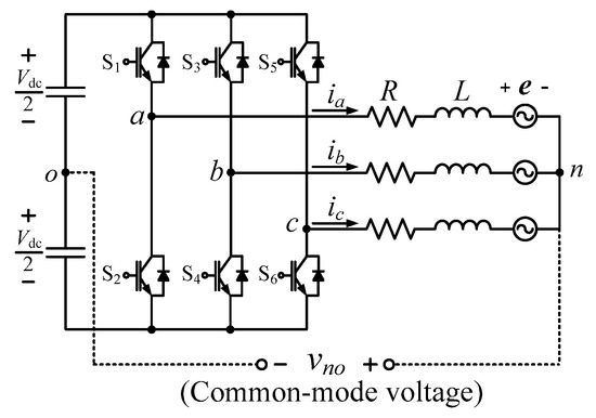
Figure 1.
Three-phase voltage-source inverter (VSI).
Figure 2 shows the eight voltage vectors that can be produced by VSIs. VSI can control the output currents by using voltage vectors [10,12]. The binary values of “0” and “1” in the switching functions indicate the open and closed states, respectively. Using the space-vector definition, the load current can be denoted as
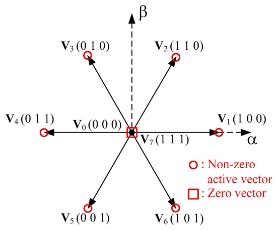
Figure 2.
Vectors generated by the VSI.
In addition, as shown in Figure 1, the CM voltage of the VSI can be defined as the potential between the center of the dc bus and the neutral point n of the VSI. The CM voltage can be denoted as [10]
The CM voltages of the VSIs becomes for the zero vectors and for the non-zero active vectors, as listed in Table 1.

Table 1.
All voltage vectors of the voltage-source inverter (VSI) and common-mode (CM) voltages according to voltage vectors.
In the VSIs, the output current dynamics can be obtained as
where , R, , L, and e represent the voltage vector, output resistance, output current vector, output inductance, and back-emf vector, respectively. Using the forward Euler approximation, the differential of the output current vector in (2) can be described in the discrete-time domain with sampling period as
In the discrete-time domain, the load current can be described as
Seven possible voltage vectors of the VSI, , generate seven possible output currents, and using (6), the future currents at the step can be obtained. Among seven possible output currents, one optimal future load current can be calculated and selected to minimize the cost function, which is predefined as the errors between the real output currents and the reference output currents at every sampling period.
Only six non-zero active vectors which generate the CM voltage within are considered in the proposed algorithm to alleviate the CM voltage, not using the zero vectors which generate CM voltage within , as indicated in Table 1. However, applying the six non-zero active vectors may worsen the three-phase output current errors and ripples because the number of available voltage vectors is reduced. It is inevitable that the current ripple is increased when the proposed algorithm controls the load current, except when the zero vectors are used, as the zero vectors typically produce the smallest variation in the load dynamics. Therefore, in one sampling period, two non-zero active vectors are used to compensate for the decreased number of candidates. The selection of two non-zero active vectors and splitting two vectors at one sampling period are determined by the proposed optimization process and updated at every sampling period. Two non-zero active vectors are selected for application to the load at every sampling period. Therefore, one sampling period can be split into two parts as
where and are the time intervals of applying non-zero active vectors and to the load, respectively, at the step. Time intervals, and , should be smaller than the sampling period Ts and larger than zero. Selecting two non-zero active vectors with changeable time intervals can lead to reduced output-current errors, output-current ripples, and CM voltage. Furthermore, optimal time intervals are determined at every sampling period. The load current at the step generated by utilizing two non-zero active vectors can be modified from (6) as
Back-emf vectors vary at much lower frequencies than sampling frequencies; therefore, at one sampling period, the back-emf vector can be presumed as
Similar to (9), by shifting (9) one step backward, the past back-emf vector at the step can be obtained as
As in the conventional method of selecting a single optimal vector, the two-step prediction is required for delay compensation technique for the calculation delay. Shifting (8) one step forward, the delay compensation technique can be attained [9] as
The future back-emf voltage vector at the step used in (11) can be obtained as
Future non-zero active vectors used in (11), and , can assume six non-zero active vectors made by the VSI, respectively. Thus, 36 possible non-zero active vector sets can be made. Therefore, the proposed algorithm can completely achieve optimal current control considering the effectiveness of two non-zero active vectors used during one sampling period and their time intervals. As a result, the proposed algorithm can be regarded as a comprehensive DV approach to alleviate the CM voltage.
The proposed scheme estimates the reference output currents and real output currents not only at the next sampling period, but also at the changing time of two active vectors. The changing time of two active vectors changes depending on each non-zero active vector set. The proposed algorithm selects one optimal vector set among the 36 possible non-zero active vector sets to minimize the cost function, which is defined as the square errors between the reference output current and real output current at two intervals, of which one is fixed and and the other is changing, as
For each non-zero active vector set, the duration of the two vectors, and , applied at and is determined by optimizing each set. The optimal time intervals, and , are divided at the future sampling period for minimizing the square errors between the reference output current and the real output current. The optimal duration can be obtained as
By reflecting on Equations (11), (13), (17), and (18) to (14), the future optimal time interval can be obtained by using (15) as
where ,
,
,
,
, and .
The remaining duration for vector can be calculated from (7) as
To compare the reference output currents and real load current at time, , of the transition from the first vector to the second, the references at time are also required. Therefore, the reference load current at time can be calculated as
Therefore, the reference output current can be attained for each voltage vector set once the time interval of the former non-zero active vector in each set is computed in (15). Similarly, the real output currents at turning time can be expressed as
After evaluating 36 possible voltage vector sets and the time distribution to minimize the cost function, one optimal future non-zero active set and their optimal durations can be selected. The two future active vectors, and , selected in the proposed scheme, are attained during the pre-selected durations and in the future sampling period. Examples of the output-current behaviors determined by voltage vectors generated by the proposed algorithm are shown in Figure 3. As shown in Figure 3, the final value of the output current depends on the voltage vector to be selected and the time intervals to be divided. The control block of the proposed algorithm is shown in Figure 4. The optimal control process for the proposed algorithm at the sampling period is attained with the following steps:
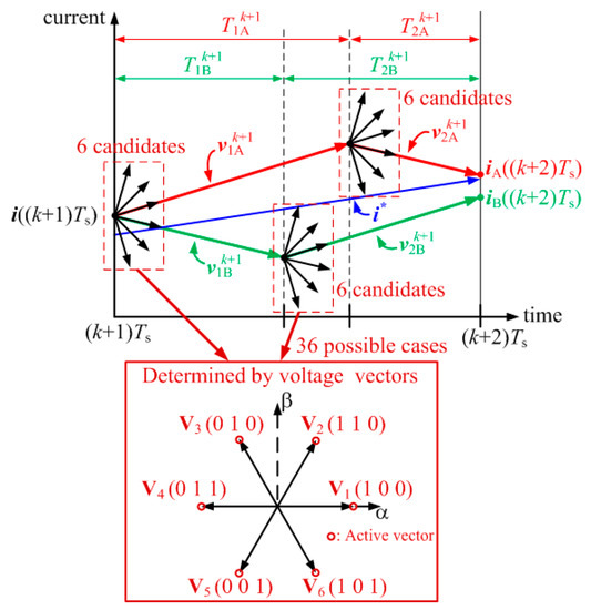
Figure 3.
Examples of output-current behaviors determined by voltage vectors generated by the proposed algorithm.
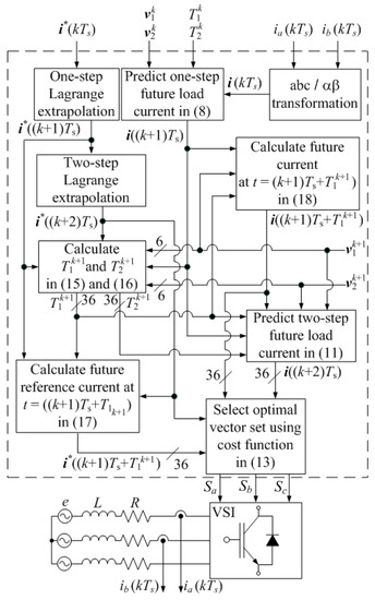
Figure 4.
Control block of the proposed algorithm.
(1) Measuring output current at the step,
(2) Predicting the future output current by applying the two nonzero active vectors and during and , respectively, which were fixed at the step by (8),
(3) Predicting the 36 possibilities for future currents and obtained by 36 possible voltage sets with non-zero vectors and along with their corresponding durations and obtained by (15) and (16),
(4) Calculating the future reference and using Lagrange extrapolation and (17), respectively,
(5) Evaluating 36 vector sets, and , and their corresponding durations, and , by utilizing the cost function in (13),
(6) Selecting one optimal set with and with their durations and ,
(7) Storing , , and for the step.
3. Simulation Results
To verify the proposed algorithm which only selects the non-zero active vectors, simulations were performed using the PSIM (power simulation) program. For comparing the performance between the proposed and conventional schemes, the simulations of the conventional method selecting one optimal voltage vector from seven different candidate vectors were also performed. The parameters are as follows: input voltage = 100 V, the amplitude of the reference = 6 A, output inductance L = 10 mH, output resistance R = 2.5 Ω and back-emf voltage e = 20 V. In addition, the proposed algorithm is operated with a sampling period = 200 μs and the conventional algorithm is operated with a half sampling period, selecting two vectors at one sampling period, for fair comparison.
Figure 5 and Figure 6 show the simulation results acquired from the proposed and conventional algorithm, respectively. The three-phase output currents of both control method are well controlled with the sinusoidal waveforms of the amplitude = 6 A as shown in Figure 5a,b. Moreover, it is observed that the CM voltage of the proposed algorithm is limited to , whereas that of the conventional method oscillates between and . Figure 5b and Figure 6b show the fast Fourier transform (FFT) spectrum of a phase output current. As shown in the figures, the proposed algorithm shows much lower harmonic components than the conventional algorithm which is operated with a half sampling frequency despite no utilization of zero vectors. This is because the optimization algorithm selects two non-zero vectors and determines their durations. Therefore, the waveforms of the proposed scheme achieve improved quality compared with those of the conventional method that operates within a half sampling period.
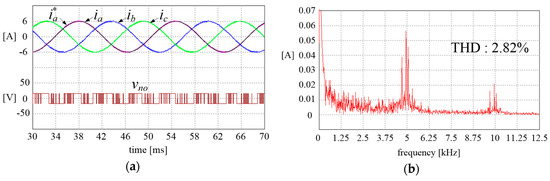
Figure 5.
Simulation results acquired from the proposed algorithm with = 200 μs: (a) the three-phase output currents (, , and ), a phase reference (), and CM voltage () (b) Fourier transform (FFT) spectrum of the a aphase output current.
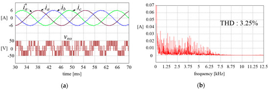
Figure 6.
Simulation results acquired from the conventional algorithm with = 100 μs: (a) the three-phase output currents (, , and ), a phase reference (), and CM voltage () (b) FFT spectrum of the a phase output current.
Figure 7 shows the dynamic response of a fundamental frequency step change acquired from the conventional and proposed algorithm. The conventional and proposed algorithms are operated with the sampling period = 100 μs and = 200 μs, respectively. In Figure 7, the fundamental frequency varied from 60 Hz to 90 Hz. The proposed algorithm can change the fundamental frequency of the currents at the same speed as the conventional algorithm as shown in Figure 7.
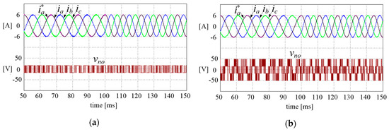
Figure 7.
Three-phase output currents (, , and ), a phase reference output current (), and CM voltage () for a fundamental frequency step change from 60 Hz to 90 Hz obtained from (a) the proposed algorithm with = 200 μs (b) the conventional algorithm with = 100 μs.
The dynamic response of an amplitude step change acquired from the conventional and proposed algorithm is shown in Figure 8. The conventional and proposed algorithms are operated with the sampling period = 100 μs and = 200 μs, respectively. In Figure 8, the amplitude of the reference varied from 9 A to 4.5 A. The three-phase output currents of the proposed scheme change as rapidly as the three-phase output currents of the conventional scheme as shown in Figure 8.
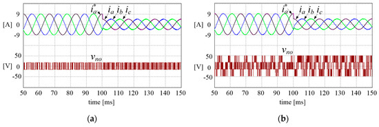
Figure 8.
Three-phase output currents (, , and ), a phase reference output current (), and CM voltage () for a amplitude step change obtained from 9 A to 4.5 A (a) the proposed algorithm with = 200 μs (b) the conventional algorithm with = 100 μs.
Because the performance of the MPC method is affected by the sampling period, the performance comparison of the four control methods which are the proposed, the conventional, DV-Con1, and DV-Con2 MPC methods from the perspective of the output-current ripples and errors versus sampling periods were added in this paper as shown in Figure 9. The DV-Con1 method and the DV-Con2 method only select non-zero active vectors like the proposed algorithm for reducing CM voltage. The output current errors attained by the conventional, DV-Con1, DV-Con2, and proposed schemes are shown in Figure 9a. The output current errors can be defined as
where the value of N was 20,000.The proposed algorithm shows lower output current error than the conventional algorithm as shown in Figure 9a. Furthermore, the current error of the proposed algorithm also shows significantly lower than those of DV-Con1 and DV-Con2 methods. Figure 9b shows the average THD percentages of output currents attained by the proposed, conventional, DV-Con1, and DV-Con2 methods. The average THD percentages of the three-phase currents can be defined as
where is the fundamental component of the output currents and is the nth-harmonic component in the x phase. The value of n was set to 8335 in the PSIM. Figure 9b shows that the THD of the proposed algorithm is much lower than that of the conventional algorithm using a half sampling period. The proposed algorithm also shows lower THD than the DV-Con1 and DV-Con2 methods using the same sampling period.
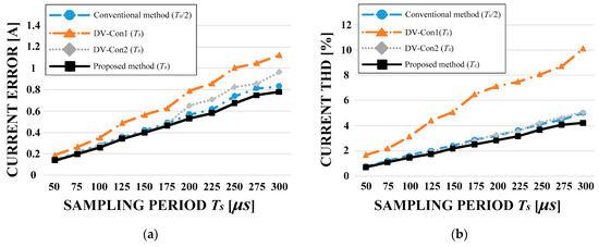
Figure 9.
Comparative results of the conventional, the DV-Con1, the DV-Con2 and the proposed algorithms versus the sampling period: (a) output-current errors, (b) total harmonic distortion (THD) of the output currents.
4. Experimental Results
A prototype setup was used to test the proposed algorithm to operate with the comprehensive DV approach and implemented in a digital signal processing (DSP) board (TMS320F28335). The proposed algorithm was operated with the sampling period = 200 μs, input dc voltage = 100 V and the amplitude of the reference = 6 A. For performance comparison, the conventional algorithm was operated with the sampling period = 100 μs which is a half sampling period of the proposed algorithm. The input dc voltage and the amplitude of the reference of the conventional algorithm are the same as those of the proposed algorithm.
Figure 10 and Figure 11 show the experimental results acquired from two control methods. The waveforms acquired from the proposed algorithm, shown in Figure 10, are similar to those of the simulation results, shown in Figure 5. The three-phase output currents of the proposed algorithm are well controlled with a sinusoidal wave, and the CM voltage is limited to because the proposed algorithm does not select the zero vectors. Otherwise, in the conventional method, the CM voltage oscillates from to , as shown in Figure 11a, because both the zero vectors and are used in the conventional algorithm. Figure 10b and Figure 11b show the FFT spectrum of the a phase current acquired from the proposed and conventional algorithm, respectively. The harmonic components of the proposed scheme are much less than that of the conventional scheme with a half sampling period as shown in Figure 10 and Figure 11. The THD and FFT spectrum of the output currents were measured from the MSO (mixed signal oscilloscope) 3054. The technical characteristics of the digital oscilloscope are shown in Table 2.
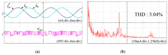
Figure 10.
Experimental results of the proposed algorithm with = 200 μs: (a) the output currents (, , and ), a phase reference (), and CM voltage () (b) FFT spectrum of the a phase output current (= 6 A and = 100 V).
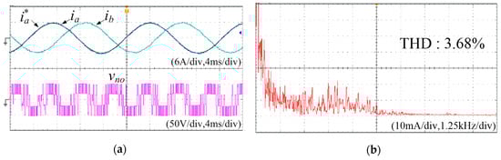
Figure 11.
Experimental results of the conventional algorithm with a half sampling period ( = 100 μs): (a) the output currents (, , and ), a phase reference (), and CM voltage (), (b) FFT spectrum of the a phase output current (= 6 A and = 100 V).
Table 2.
The technical characteristics of the MSO (mixed signal oscilloscope) 3054.
Figure 12 shows the experimental waveforms of the dynamic responses of a fundamental frequency step change obtained from the conventional and proposed algorithm. The conventional and proposed algorithms are operated with the sampling period = 100 μs and = 200 μs, respectively. In Figure 12, the fundamental frequency of the reference varied from 60 Hz to 90 Hz. The proposed algorithm can change the fundamental frequency of the three-phase output currents at the same speed as the conventional algorithm as shown in Figure 12.
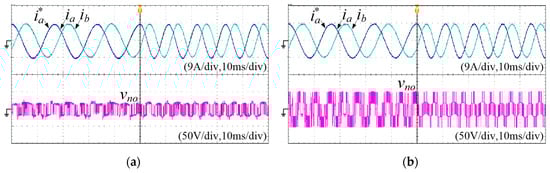
Figure 12.
Experimental results of the output currents ( and ), a phase reference (), and the CM voltage () for a fundamental frequency step change from 60 Hz to 90 Hz for (a) the proposed algorithm with = 200 μs, (b) the conventional algorithm with = 100 μs.
The experimental waveforms of the dynamic responses of an amplitude step change acquired from the conventional and the proposed algorithm are shown in Figure 13. The conventional and the proposed algorithms are operated with the sampling period = 100 μs and = 200 μs, respectively. In Figure 13, the magnitude of the reference varied from 9 A to 4.5 A. As shown in Figure 13, the proposed algorithm can change the amplitude of three-phase output currents at the same speed as the conventional algorithm.
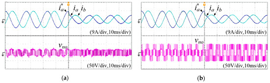
Figure 13.
Experimental results of the output currents ( and ), a phase reference current (), and the CM voltage () for a amplitude step change from 9 A to 4.5 A for (a) the proposed algorithm with = 200 μs, (b) the conventional algorithm with = 100 μs.
5. Conclusions
This paper proposed a comprehensive DV approach for VSI based on the MPC algorithm for reducing the CM voltage. Two non-zero active vectors were chosen and partitioned in one sampling period through the optimization process at every sampling instant, by considering all 36 possible combinations producible by two non-zero active vectors of the three-phase VSI in the proposed algorithm. The zero vectors produced the highest CM voltage; therefore the proposed algorithm only selected non-zero active vectors. Based on the optimal process for distributing and applying two active vectors during one sampling period, the proposed algorithm was able to decrease the output-current ripple, output-current error, and the CM voltage. The current ripples and errors of the proposed algorithm were also lower than those of the DV-Con1 and DV-Con2 methods that use a DV. The proposed algorithm can also control the output current with a rapid transient response. The proposed algorithm was validated by simulation and experimental results.
Author Contributions
Conceptualization, S.K.; methodology, S.K.; software, S.-y.P.; validation, S.-y.P. and E.-S.J.; Writing—Original Draft preparation, S.-y.P.; Writing—Review and Editing, E.-S.J.; visualization, E.-S.J.; supervision, S.K.; project administration, S.K.; funding acquisition, S.K.
Funding
This research was supported by the National Research Foundation of Korea (NRF) grant funded by the Korean government (MSIP) (2017R1A2B4011444) and the Human Resources Development (No.20174030201810) of the Korea Institute of Energy Technology Evaluation and Planning (KETEP) grant funded by the Korea government Ministry of Trade, Industry and Energy.
Conflicts of Interest
The authors declare no conflict of interest.
References
- Kazmierkowski, M.P.; Krishnan, R.; Blaabjerg, F. Control in Power Electronics; Kazmierkowski, M.P., Krishnan, R., Eds.; Academic Press: New York, NY, USA, 2002. [Google Scholar]
- Mohan, N.; Underland, T.M.; Robbins, W.P. Power Electronics, 2nd ed.; John Wiley & Sons: Hoboken, NJ, USA, 1989. [Google Scholar]
- Takahashi, S.; Ogasawara, S.; Takemoto, M.; Orikawa, K.; Tamate, M. Common-Mode Voltage Attenuation of an Active Common-Mode Filter in a Motor Drive System Fed by a PWM Inverter. IEEE Trans. Ind. Appl. 2019, 55, 2721–2730. [Google Scholar] [CrossRef]
- Kwak, S.; Mun, S. Common-mode voltage mitigation with a predictive control method considering dead time effects of three-phase voltage source inverters. IET Power Electron. 2015, 8, 1690–1700. [Google Scholar] [CrossRef]
- Chen, W.; Yang, X.; Wang, Z. A novel hybrid common-mode EMI filter with active impedance multiplication. IEEE Trans. Ind. Electron. 2011, 58, 1826–1834. [Google Scholar] [CrossRef]
- Mun, S.; Kwak, S. Reducing common-mode voltage of three-phase VSIs using the predictive current control method based on reference voltage. J. Power Electron. 2015, 15, 712–720. [Google Scholar] [CrossRef]
- Arora, T.G.; Renge, M.M.; Aware, M.V. Effects of switching frequency and motor speed on common mode voltage, common mode current and shaft voltage in PWM inverter-fed induction motors. In Proceedings of the 12th IEEE Conference on Industrial Electronics and Applications (ICIEA, 2017), Siem Reap, Cambodia, 18–20 June 2017; pp. 2158–2297. [Google Scholar] [CrossRef]
- Kwak, S.; Mun, S.-k. Model predictive control methods to reduce common-mode voltage for three-phase voltage source inverters. IEEE Trans. Power Electron. 2015, 30, 5019–5035. [Google Scholar] [CrossRef]
- Duran, M.J.; Riveros, J.A.; Barrero, F.; Guzman, H.; Prieto, J. Reduction of Common-Mode Voltage in Five-Phase Induction Motor Drives Using Predictive Control Techniques. IEEE Trans. Ind. Appl. 2012, 48, 2059–2067. [Google Scholar] [CrossRef]
- Kimball, J.W.; Zawodniok, M. Reducing Common-Mode Voltage in Three-Phase Sine-Triangle PWM With Interleaved Carriers. IEEE Trans. Power Electron. 2011, 26, 2229–2236. [Google Scholar] [CrossRef]
- Huang, J.; Shi, H. Suppressing low-frequency components of common-mode voltage through reverse injection in three-phase inverter. IET Power Electron. 2014, 7, 1644–1653. [Google Scholar] [CrossRef]
- Hoseini, S.K.; Sheikholeslami, A.; Adabi, J. Predictive modulation schemes to reduce common-mode voltage in three-phase inverters-fed AC drive systems. IET Power Electron. 2014, 7, 840–849. [Google Scholar] [CrossRef]
- Hava, A.; Un, E. Performance Analysis of Reduced Common-Mode Voltage PWM Methods and Comparison With Standard PWM Methods for Three-Phase Voltage-Source Inverters. IEEE Trans. Power Electron. 2009, 24, 241–252. [Google Scholar] [CrossRef]
- Hou, C.-C.; Shih, C.-C.; Cheng, P.-T.; Hava, A.M. Common-mode voltage reduction pulsewidth modulation techniques for three-phase grid-connected converters. IEEE Trans. Power Electron. 2013, 28, 1971–1979. [Google Scholar] [CrossRef]
- Adabi, J.; Ghosh, A.; Nami, A.; Boora, A.; Zare, F.; Blaabjerg, F. Common-mode voltage reduction in a motor drive system with a power factor correction. IET Power Electron. 2012, 5, 366–375. [Google Scholar] [CrossRef]
- Guo, L.; Zhang, X.; Yang, S.; Xie, Z.; Cao, R. A Model Predictive Control-Based Common-Mode Voltage Suppression Strategy for Voltage-Source Inverter. IEEE Trans. Ind. Electron. 2016, 63, 6115–6125. [Google Scholar] [CrossRef]
- Park, S.Y.; Kwak, S. Comparative study of three model predictive current control methods with two vectors for three-phase DC/AD VSIs. IET Electron. Power Appl. 2017, 11, 1284–1297. [Google Scholar] [CrossRef]
- Jun, E.-S.; Park, S.-y.; Kwak, S. Model predictive current control method with improved performances for three-phase voltage source inverters. Electronics. 2019, 8. [Google Scholar] [CrossRef]
- Guzman, R.; De Vicuna, L.G.; Camacho, A.; Miret, J.; Rey, J.M. Receding-Horizon Model-Predictive Control for a Three-Phase VSI With an LCL Filter. IEEE Trans. Ind. Electron. 2019, 66, 6671–6680. [Google Scholar] [CrossRef]
- Zhou, Y.; Li, H.; Liu, R.; Mao, J. Continuous Voltage Vector Model-Free Predictive Current Control of Surface Mounted Permanent Magnet Synchronous Motor. IEEE Trans. Energy Convers. 2019, 34, 899–908. [Google Scholar] [CrossRef]
- Khan, S.A.; Guo, Y.; Zhu, J. Model predictive observer based control for single-phase asymmetrical T-type AC/DC power converte. IEEE Trans. Indus. Appl. 2019, 55, 2033–2044. [Google Scholar] [CrossRef]
- Novak, M.; Dragicevic, T.; Blaabjerg, F. Weighting factor design based on Artificial Neural Network for Finite Set MPC operated 3L-NPC converter. In Proceedings of the 2019 IEEE Applied Power Electronics Conference and Exposition (APEC, 2019), Anaheim, CA, USA, 17–21 March 2019. [Google Scholar] [CrossRef]
- Tavernini, D.; Metzler, M.; Gruber, P.; Sorniotti, A. Explicit nonlinear model predictive control for electric vehicle traction control. IEEE Trans. Control Syst. Tech. 2019, 27, 1438–1451. [Google Scholar] [CrossRef]
- Makhamreh, H.; Sleiman, M.; Kukrer, O.; Al-Haddad, K. Lyapunov-Based Model Predictive Control of a PUC7 Grid-Connected Multilevel Inverter. IEEE Trans. Ind. Electron. 2019, 66, 7012–7021. [Google Scholar] [CrossRef]
- He, Z.; Guo, P.; Shuai, Z.; Xu, Q.; Luo, A.; Guerrero, J.M. Modulated Model Predictive Control for Modular Multilevel AC/AC Converter. IEEE Trans. Power Electron. 2019, 34, 10359–10372. [Google Scholar] [CrossRef]
- Zhang, S.; Madawala, U.K. A hybrid model predictive multilayer control strategy for modular multilevel converters. IEEE J. Emerging Sel. Top. Power Electron. 2019, 7, 1002–1014. [Google Scholar] [CrossRef]
- Gontijo, G.F.; Tricarico, T.C.; Franca, B.W.; Da Silva, L.F.; Van Emmerik, E.L.; Aredes, M. Robust Model Predictive Rotor Current Control of a DFIG Connected to a Distorted and Unbalanced Grid Driven by a Direct Matrix Converter. IEEE Trans. Sustain. Energy 2019, 10, 1380–1392. [Google Scholar] [CrossRef]
- Gulbudak, O.; Santi, E. FPGA-based model predictive controller for direct matrix converter. IEEE Trans. Ind. Electron. 2016, 63, 4560–4570. [Google Scholar] [CrossRef]
- Chen, X.; Liu, J.; Song, S.; Ouyang, S.; Wu, H.; Yang, Y. Modified increased-level model predictive control methods with reduced computation load for modular multilevel converter. IEEE Trans. Power Electron. 2019, 34, 7310–7325. [Google Scholar] [CrossRef]
- Mora, A.; Urrutia, M.; Cardenas, R.; Angulo, A. Model-predictive-control-based capacitor voltage balancing strategies for modular multilevel converters. IEEE Trans. Indus. Electron. 2019, 66, 2432–2443. [Google Scholar] [CrossRef]
© 2019 by the authors. Licensee MDPI, Basel, Switzerland. This article is an open access article distributed under the terms and conditions of the Creative Commons Attribution (CC BY) license (http://creativecommons.org/licenses/by/4.0/).