1. Introduction
Three-phase voltage-source inverters (VSIs) have been used commonly to generate three-phase line currents, while the frequencies and amplitude of the three-phase line currents are changeable [
1,
2]. In VSIs, the fast switching operation results in common-mode (CM) voltage, which has been considered the cause of over voltage stress to surrounding electronic systems [
3,
4,
5,
6,
7,
8]. To alleviate the amplitude of the CM voltage, multifarious studies have been conducted with a PWM algorithm that is designed by only selecting the non-zero active vectors, and this is because the zero vectors produce the highest CM voltage [
3,
4,
5,
6,
7,
8]. However, when the inverter is controlled by only using the non-zero active vectors without selecting the zero vectors, the Total Harmonic Distortion (THD) and error of the output currents of the inverter inevitably deteriorate. This is because zero vectors typically produce the smallest variation in the load dynamics. Therefore, methods for reducing the CM voltage without deteriorating the inverter performance have been studied extensively [
9,
10,
11,
12,
13,
14,
15,
16]. Recently, a model predictive control (MPC) method was studied for VSIs owing to its flexibility and simplicity of control [
17,
18,
19,
20,
21,
22,
23,
24,
25,
26,
27,
28,
29]. Utilizing the basic principle that VSIs can apply two zero vectors and six different non-zero active voltage vectors to the load, seven different future current behaviors, which change according to the voltage vectors, can be predicted by the MPC method. The possible future currents of the VSI can be calculated using the load dynamic model. Based on the cost function, which is predefined as the error between the reference currents and the predicted output currents, all predicted currents calculated by the seven different possible cases using the load dynamic model can be used to choose one voltage vector to minimize the predefined cost function. However, in the conventional MPC method which selects only one voltage vector during the sampling period, if only the active vector is used to reduce the CM voltage without using a zero vector which produces the highest CM voltage, the current error and current total harmonic distortion (THD) are inevitably higher than those of the method using PWM blocks. To overcome these problems, MPC methods using a double vector (DV) have been studied [
8,
17,
18]. In this paper, there are two conventional DV-MPC algorithms, called DV-Conv1 and DV-Conv2. In the DV-Con1 method, two vectors closest to the reference are first selected, and then the sampling period is divided for minimizing the cost function [
10]. In the DV-Con2 method, one vector closest to the reference vector is selected first, and the second vector is selected by dividing the sampling period to minimize the cost function [
8,
17,
18]. However, such control methods have a disadvantage in that the calculation time is increased and if the conventional algorithm is operated with a half sampling period, selecting two vectors at one sampling period, for fair comparison, the current ripples and errors of the DV-Con1 and DV-Con2 methods are higher than those of the conventional method which selects one vector during one sampling period. Finally, the VSI using the MPC method applies the optimal voltage vector during each sampling period. Because of its simplicity, the MPC method has been used extensively to control the line current of many non-VSI converters, which are matrix converters, multiphase inverters, and multilevel inverters [
19,
20,
21,
22,
23,
24,
25,
26,
27,
28,
29,
30].
This paper proposes a comprehensive DV method to mitigate the CM voltage in VSIs based on the MPC scheme. Only six active vectors are utilized to control currents to alleviate the CM voltage in the proposed algorithm, because the zero vector makes the highest CM voltage. Therefore, the proposed algorithm can alleviate the CM voltage within except for the two zero vectors which make the CM voltage within . Furthermore, the proposed algorithm uses two non-zero active vectors at one sampling period to compensate for the decreased number of candidates. The proposed algorithm selects two non-zero active vectors and divides them within one sampling period by considering all 36 possible combinations produced by the six non-zero active vectors to minimize the predefined cost function. This optimization process can minimize current ripples and errors. The proposed algorithm makes small current ripples and errors compared with the conventional algorithm despite not using zero vectors. The proposed algorithm also has a better control performance compared with the DV-Con1 method and DV-Con2 method because the proposed algorithm considers more cases than the two methods. Furthermore, as a solution to the computation time delay, the delay compensation technique was used in the proposed algorithm. In addition, the zero vectors are not selected in the normal transient condition, therefore the proposed algorithm does not adversely affect the fast transient response. To verify the proposed algorithm, simulation and experiment were performed.
2. Conventional Model Predictive Current Control Method for VSIs
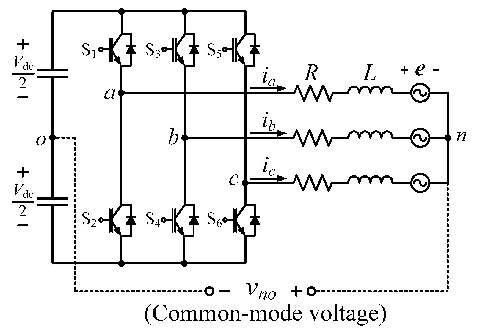
Figure 1 shows the three-phase VSI, where the voltage vector applied to the load can be denoted as
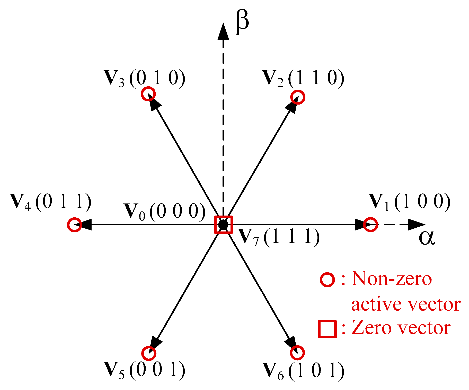
Figure 2 shows the eight voltage vectors that can be produced by VSIs. VSI can control the output currents by using voltage vectors [
10,
12]. The binary values of “0” and “1” in the switching functions indicate the open and closed states, respectively. Using the space-vector definition, the load current can be denoted as
In addition, as shown in
Figure 1, the CM voltage of the VSI can be defined as the potential between the center of the dc bus and the neutral point
n of the VSI. The CM voltage can be denoted as [
10]
The CM voltages of the VSIs becomes
for the zero vectors and
for the non-zero active vectors, as listed in
Table 1.
In the VSIs, the output current dynamics can be obtained as
where
,
R,
, L, and
e represent the voltage vector, output resistance, output current vector, output inductance, and back-emf vector, respectively. Using the forward Euler approximation, the differential of the output current vector in (2) can be described in the discrete-time domain with sampling period
as
In the discrete-time domain, the load current can be described as
Seven possible voltage vectors of the VSI, , generate seven possible output currents, and using (6), the future currents at the step can be obtained. Among seven possible output currents, one optimal future load current can be calculated and selected to minimize the cost function, which is predefined as the errors between the real output currents and the reference output currents at every sampling period.
Only six non-zero active vectors which generate the CM voltage within
are considered in the proposed algorithm to alleviate the CM voltage, not using the zero vectors which generate CM voltage within
, as indicated in
Table 1. However, applying the six non-zero active vectors may worsen the three-phase output current errors and ripples because the number of available voltage vectors is reduced. It is inevitable that the current ripple is increased when the proposed algorithm controls the load current, except when the zero vectors are used, as the zero vectors typically produce the smallest variation in the load dynamics. Therefore, in one sampling period, two non-zero active vectors are used to compensate for the decreased number of candidates. The selection of two non-zero active vectors and splitting two vectors at one sampling period are determined by the proposed optimization process and updated at every sampling period. Two non-zero active vectors are selected for application to the load at every sampling period. Therefore, one sampling period can be split into two parts as
where
and
are the time intervals of applying non-zero active vectors
and
to the load, respectively, at the
step. Time intervals,
and
, should be smaller than the sampling period
Ts and larger than zero. Selecting two non-zero active vectors with changeable time intervals can lead to reduced output-current errors, output-current ripples, and CM voltage. Furthermore, optimal time intervals are determined at every sampling period. The load current at the
step generated by utilizing two non-zero active vectors can be modified from (6) as
Back-emf vectors vary at much lower frequencies than sampling frequencies; therefore, at one sampling period, the back-emf vector can be presumed as
Similar to (9), by shifting (9) one step backward, the past back-emf vector at the
step can be obtained as
As in the conventional method of selecting a single optimal vector, the two-step prediction is required for delay compensation technique for the calculation delay. Shifting (8) one step forward, the delay compensation technique can be attained [
9] as
The future back-emf voltage vector at the
step used in (11) can be obtained as
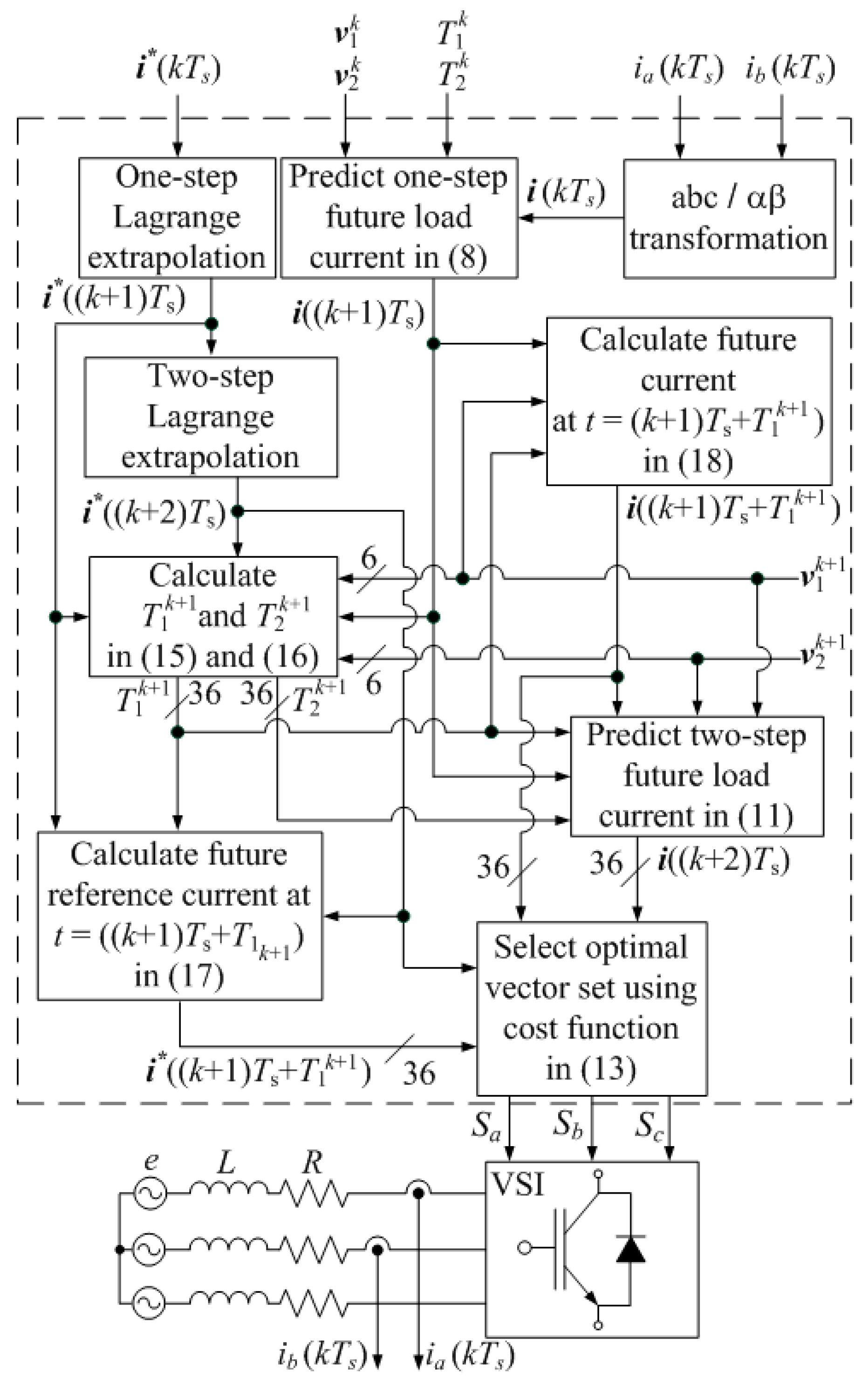
Future non-zero active vectors used in (11), and , can assume six non-zero active vectors made by the VSI, respectively. Thus, 36 possible non-zero active vector sets can be made. Therefore, the proposed algorithm can completely achieve optimal current control considering the effectiveness of two non-zero active vectors used during one sampling period and their time intervals. As a result, the proposed algorithm can be regarded as a comprehensive DV approach to alleviate the CM voltage.
The proposed scheme estimates the reference output currents and real output currents not only at the next sampling period, but also at the changing time of two active vectors. The changing time of two active vectors changes depending on each non-zero active vector set. The proposed algorithm selects one optimal vector set among the 36 possible non-zero active vector sets to minimize the cost function, which is defined as the square errors between the reference output current and real output current at two intervals, of which one is fixed and and the other is changing, as
For each non-zero active vector set, the duration of the two vectors,
and
, applied at
and
is determined by optimizing each set. The optimal time intervals,
and
, are divided at the future sampling period for minimizing the square errors between the reference output current and the real output current. The optimal duration can be obtained as
By reflecting on Equations (11), (13), (17), and (18) to (14), the future optimal time interval
can be obtained by using (15) as
where
,
,
,
,
, and .
The remaining duration
for vector
can be calculated from (7) as
To compare the reference output currents and real load current at time,
, of the transition from the first vector to the second, the references at time
are also required. Therefore, the reference load current at time
can be calculated as
Therefore, the reference output current
can be attained for each voltage vector set once the time interval of the former non-zero active vector in each set
is computed in (15). Similarly, the real output currents at turning time
can be expressed as
After evaluating 36 possible voltage vector sets and the time distribution to minimize the cost function, one optimal future non-zero active set and their optimal durations can be selected. The two future active vectors,
and
, selected in the proposed scheme, are attained during the pre-selected durations
and
in the future sampling period. Examples of the output-current behaviors determined by voltage vectors generated by the proposed algorithm are shown in
Figure 3. As shown in
Figure 3, the final value of the output current depends on the voltage vector to be selected and the time intervals to be divided. The control block of the proposed algorithm is shown in
Figure 4. The optimal control process for the proposed algorithm at the
sampling period is attained with the following steps:
(1) Measuring output current at the step,
(2) Predicting the future output current by applying the two nonzero active vectors and during and , respectively, which were fixed at the step by (8),
(3) Predicting the 36 possibilities for future currents and obtained by 36 possible voltage sets with non-zero vectors and along with their corresponding durations and obtained by (15) and (16),
(4) Calculating the future reference and using Lagrange extrapolation and (17), respectively,
(5) Evaluating 36 vector sets, and , and their corresponding durations, and , by utilizing the cost function in (13),
(6) Selecting one optimal set with and with their durations and ,
(7) Storing , , and for the step.
3. Simulation Results
To verify the proposed algorithm which only selects the non-zero active vectors, simulations were performed using the PSIM (power simulation) program. For comparing the performance between the proposed and conventional schemes, the simulations of the conventional method selecting one optimal voltage vector from seven different candidate vectors were also performed. The parameters are as follows: input voltage = 100 V, the amplitude of the reference = 6 A, output inductance L = 10 mH, output resistance R = 2.5 Ω and back-emf voltage e = 20 V. In addition, the proposed algorithm is operated with a sampling period = 200 μs and the conventional algorithm is operated with a half sampling period, selecting two vectors at one sampling period, for fair comparison.
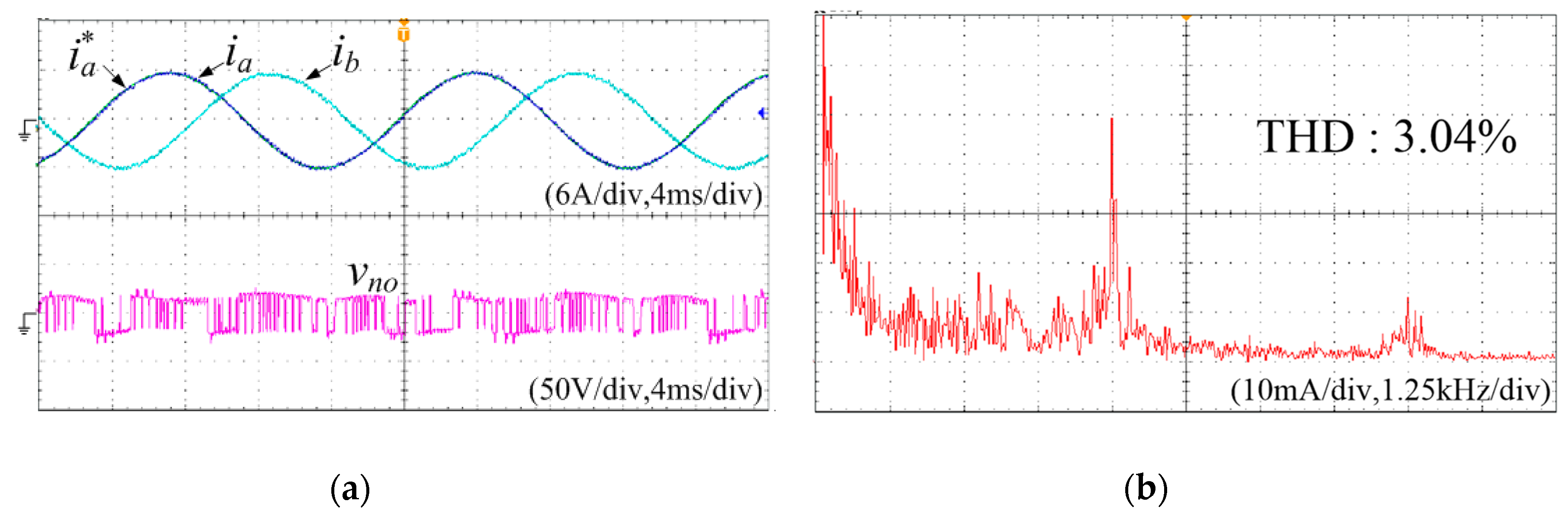
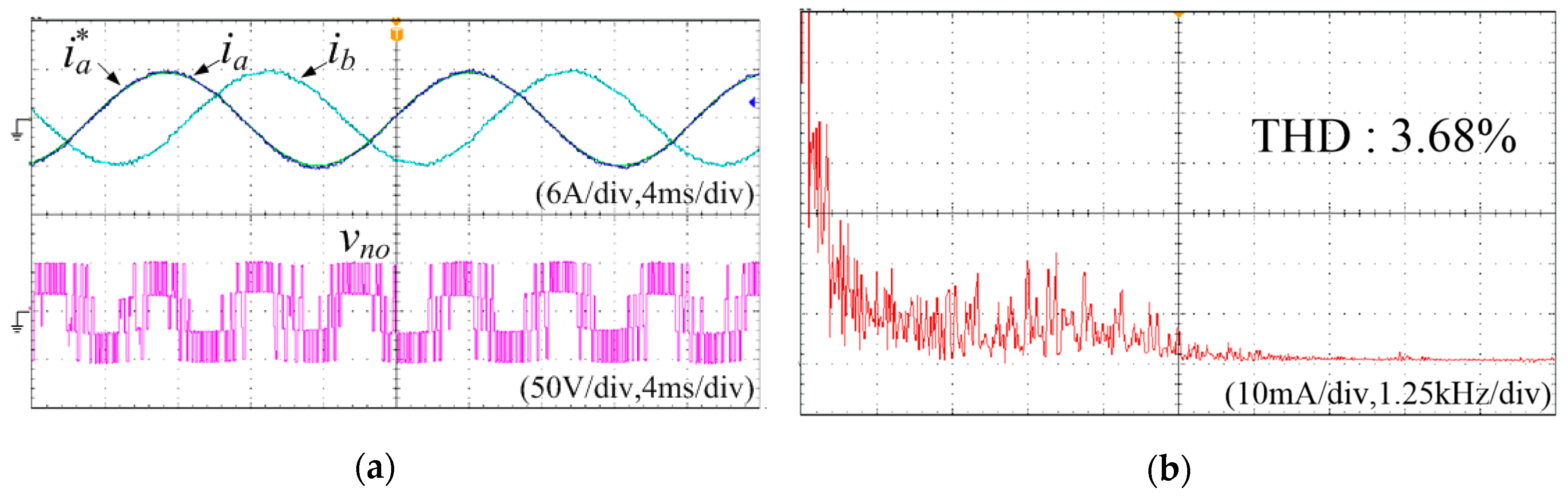
Figure 5 and
Figure 6 show the simulation results acquired from the proposed and conventional algorithm, respectively. The three-phase output currents of both control method are well controlled with the sinusoidal waveforms of the amplitude
= 6 A as shown in
Figure 5a,b. Moreover, it is observed that the CM voltage of the proposed algorithm is limited to
, whereas that of the conventional method oscillates between
and
.
Figure 5b and
Figure 6b show the fast Fourier transform (FFT) spectrum of
a phase output current. As shown in the figures, the proposed algorithm shows much lower harmonic components than the conventional algorithm which is operated with a half sampling frequency despite no utilization of zero vectors. This is because the optimization algorithm selects two non-zero vectors and determines their durations. Therefore, the waveforms of the proposed scheme achieve improved quality compared with those of the conventional method that operates within a half sampling period.
Figure 7 shows the dynamic response of a fundamental frequency step change acquired from the conventional and proposed algorithm. The conventional and proposed algorithms are operated with the sampling period
= 100
μs and
= 200
μs, respectively. In
Figure 7, the fundamental frequency varied from 60 Hz to 90 Hz. The proposed algorithm can change the fundamental frequency of the currents at the same speed as the conventional algorithm as shown in
Figure 7.
The dynamic response of an amplitude step change acquired from the conventional and proposed algorithm is shown in
Figure 8. The conventional and proposed algorithms are operated with the sampling period
= 100
μs and
= 200
μs, respectively. In
Figure 8, the amplitude of the reference varied from 9 A to 4.5 A. The three-phase output currents of the proposed scheme change as rapidly as the three-phase output currents of the conventional scheme as shown in
Figure 8.
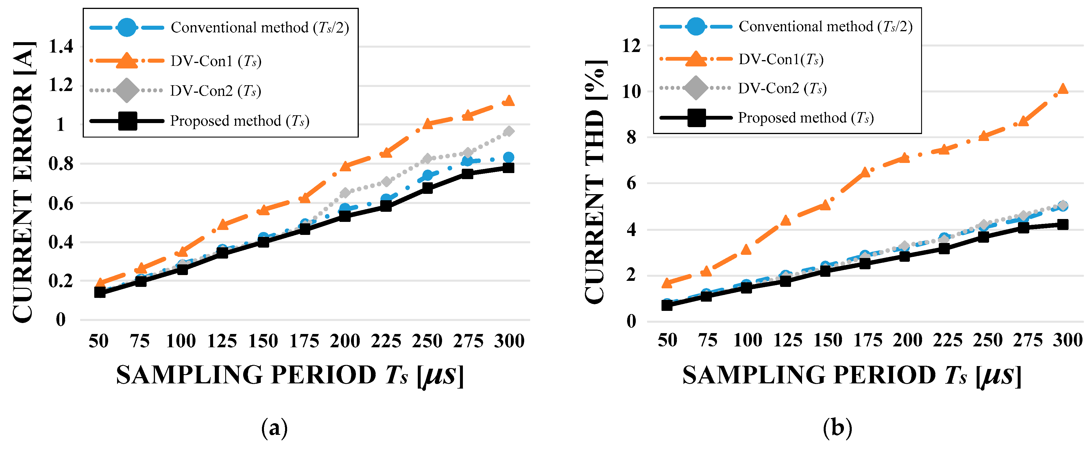
Because the performance of the MPC method is affected by the sampling period, the performance comparison of the four control methods which are the proposed, the conventional, DV-Con1, and DV-Con2 MPC methods from the perspective of the output-current ripples and errors versus sampling periods were added in this paper as shown in
Figure 9. The DV-Con1 method and the DV-Con2 method only select non-zero active vectors like the proposed algorithm for reducing CM voltage. The output current errors attained by the conventional, DV-Con1, DV-Con2, and proposed schemes are shown in
Figure 9a. The output current errors can be defined as
where the value of
N was 20,000.The proposed algorithm shows lower output current error than the conventional algorithm as shown in
Figure 9a. Furthermore, the current error of the proposed algorithm also shows significantly lower than those of DV-Con1 and DV-Con2 methods.
Figure 9b shows the average THD percentages of output currents attained by the proposed, conventional, DV-Con1, and DV-Con2 methods. The average THD percentages of the three-phase currents can be defined as
where
is the fundamental component of the output currents and
is the
nth-harmonic component in the
x phase. The value of
n was set to 8335 in the PSIM.
Figure 9b shows that the THD of the proposed algorithm is much lower than that of the conventional algorithm using a half sampling period. The proposed algorithm also shows lower THD than the DV-Con1 and DV-Con2 methods using the same sampling period.
4. Experimental Results
A prototype setup was used to test the proposed algorithm to operate with the comprehensive DV approach and implemented in a digital signal processing (DSP) board (TMS320F28335). The proposed algorithm was operated with the sampling period = 200 μs, input dc voltage = 100 V and the amplitude of the reference = 6 A. For performance comparison, the conventional algorithm was operated with the sampling period = 100 μs which is a half sampling period of the proposed algorithm. The input dc voltage and the amplitude of the reference of the conventional algorithm are the same as those of the proposed algorithm.
Figure 10 and
Figure 11 show the experimental results acquired from two control methods. The waveforms acquired from the proposed algorithm, shown in
Figure 10, are similar to those of the simulation results, shown in
Figure 5. The three-phase output currents of the proposed algorithm are well controlled with a sinusoidal wave, and the CM voltage
is limited to
because the proposed algorithm does not select the zero vectors. Otherwise, in the conventional method, the CM voltage oscillates from
to
, as shown in
Figure 11a, because both the zero vectors
and
are used in the conventional algorithm.
Figure 10b and
Figure 11b show the FFT spectrum of the
a phase current acquired from the proposed and conventional algorithm, respectively. The harmonic components of the proposed scheme are much less than that of the conventional scheme with a half sampling period as shown in
Figure 10 and
Figure 11. The THD and FFT spectrum of the output currents were measured from the MSO (mixed signal oscilloscope) 3054. The technical characteristics of the digital oscilloscope are shown in
Table 2.
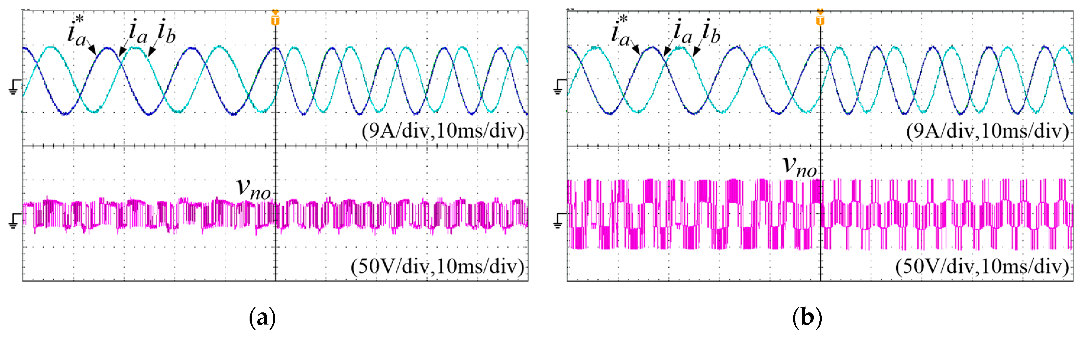
Figure 12 shows the experimental waveforms of the dynamic responses of a fundamental frequency step change obtained from the conventional and proposed algorithm. The conventional and proposed algorithms are operated with the sampling period
= 100
μs and
= 200
μs, respectively. In
Figure 12, the fundamental frequency of the reference varied from 60 Hz to 90 Hz. The proposed algorithm can change the fundamental frequency of the three-phase output currents at the same speed as the conventional algorithm as shown in
Figure 12.
The experimental waveforms of the dynamic responses of an amplitude step change acquired from the conventional and the proposed algorithm are shown in
Figure 13. The conventional and the proposed algorithms are operated with the sampling period
= 100
μs and
= 200
μs, respectively. In
Figure 13, the magnitude of the reference varied from 9 A to 4.5 A. As shown in
Figure 13, the proposed algorithm can change the amplitude of three-phase output currents at the same speed as the conventional algorithm.


