Article

Active Power Decoupling Design of a Single-Phase AC–DC Converter

School of Electrical and Information Engineering, Tianjin University, Tianjin 300072, China
*
Author to whom correspondence should be addressed.
Electronics 2019, 8(8), 841; https://doi.org/10.3390/electronics8080841
Submission received: 12 June 2019 / Revised: 19 July 2019 / Accepted: 22 July 2019 / Published: 27 July 2019
(This article belongs to the Special Issue Advanced Power Conversion Technologies)

Abstract

:
The second-order ripple power of single-phase converter causes second-order ripple voltages on the DC bus. For eliminating second-order ripple components, passive power decoupling methods including DC bus electrolytic capacitors have some shortcomings, such as low power density and poor stability of converters. Thus, an active power decoupling method based on a single-phase converter is proposed in this paper. The control method, taking single-phase voltage source pulse width modulation (PWM) rectifier (single-phase VSR) as the basic converter and adopting a buck-boost power decoupling circuit, introduces second-order ripple of DC bus voltage into a power decoupling circuit. The ripple acts as compensation of the phase deviation between the command value and the actual value of the second-order ripple current. Therefore, estimation of the second-order ripple current is more accurate, the power decoupling circuit absorbs the second-order ripple power behind the H-bridge more completely, and the DC bus voltage ripple is effectively suppressed accordingly. Finally, experimental results of the single-phase VSR are given to verify the validity of the proposed method.

1. Introduction

Single-phase voltage source pulse width modulation (PWM) converters are widely used in uninterruptible power supply, locomotive traction, DC microgrids, and renewable energy systems because of its high efficiency and reliability [1,2,3,4,5]. However, the unbalance of instantaneous active power between DC and AC sides of the single-phase converter puts inevitable second-order components of the voltage and power on the DC bus, which endangers the operation of equipment and system [6,7]. In order to reduce the fluctuation of voltage and power on the DC side, the most common way is to install passive power decoupling systems on the DC side, such as large capacitors or LC filters. LC filter refers to a resonant branch consisting of an inductor and a capacitor in series. A reasonable parameter design will make the resonant frequency of this branch twice the power frequency. As a result, the second-order ripple power is completely transferred to the LC filter. Nevertheless, passive power decoupling systems always need large capacitors, especially in high-voltage and high-power situations. In addition, for the specific systems pursuing a high power density or lighter weight, small capacitors are preferable. Another factor is the limited lifetime of large electrolytic capacitors, which leads to reliability problems and increases maintenance costs [8,9,10]. To solve the above problems, some scholars put forward the active power decoupling method [11,12,13,14,15,16]. Active power decoupling circuits include switches and storage systems. By controlling the on/off states of switches, the conversion between the second-order ripple energy of the DC bus and the energy of storage element in the power decoupling circuit is realized. This method greatly reduces system volume and prolongs the service life of the system.
In recent years, research on active power decoupling has emerged [17,18,19], which can be divided into dependent power decoupling circuits (DPDCs) [20,21,22,23,24,25,26] and independent power decoupling circuits (IPDCs) [27,28,29,30,31,32,33]. DPDCs ordinarily multiplex the power switches with the H-bridge arm of the converter. In [20], a buck-type DPDC is analyzed in detail, and the corresponding direct power decoupling method and automatic power decoupling method are proposed. Like other DPDCs, the applied decoupling circuit in [20] reduced the cost and volume of the system. However, due to the coupling between the control of the decoupling circuit and the H-bridge arm, this method becomes more complex. In contrast, IPDCs are more flexible to control. IPDCs refer to the topologies in which operation of the power decoupling circuits is independent of the single-phase converters. The circuits in [27,28,29,30,31,32,33] met this requirement. In [30,31], a boost-type IPDC is considered. The proposed estimation method of second-order ripple current ignores the probable phase deviation of AC input voltage and input current, which results in incomplete absorption of second-order ripple power. Authors in [32] consider the deviation, but estimation of the second-order ripple current of the DC side derives from the output of the converter controller; thus, control of the decoupling circuit and the converter loop is coupled. In order to obtain second-order ripple currents accurately, the pulsating current after flowing through the H-bridge is directly sampled by the authors in [33]. As a result, this method places high demands on the switching frequency and accuracy of sampling.
Considering the complexity of DPDC and the imprecision of estimation, a control strategy based on an IPDC buck-boost-type power decoupling circuit is proposed in this paper. The second-order ripple of DC bus voltage is introduced to control the decoupling inductor current. The advantage of this control method is that the phase deviations of H-bridge voltage and AC current are considered. Thus, the estimation is more accurate, and the second-order ripple of the DC bus voltage and power is effectively suppressed accordingly. The selected buck-boost-type power decoupling topology allows the voltage across the decoupling capacitor to vary depending on the output voltage range of the rectifier; the decoupling capacitance can, therefore, be flexibly changed. Authors in [33] select the same power decoupling topology. However, the decoupling loop works in continuous current mode (CCM) in this paper, while paper [33], which applied the same buck-boost-type power decoupling circuit, works in (discontinuous current mode) DCM. Control in CCM reduces the current stress of power switches. In addition, the second-order ripple current is obtained by estimation rather than sampling, as in paper [33], which avoids the difficulty of high-frequency sampling. Moreover, the closed-loop regulation can eliminate steady-state error in real time, which has a strong anti-interference ability and good dynamic characteristics. This avoids the neglect of parasitic parameters and external interference in an open-loop control circuit [33]. To simplify the experiment, the single-phase voltage source PWM rectifier (single-phase VSR) is analyzed in this paper. Though, the proposed method is also applicable to single-phase voltage source PWM inverters with front stages, such as (Photovoltaic) PV inverters.
The power distribution of the rectifier is analyzed firstly. Secondly, the characteristics of the buck-boost-type power decoupling circuit and the other two decoupling circuits are compared. The control strategy of power decoupling circuit is further introduced in the third part. Then, the parameter design of power decoupling circuit is given in CCM. Finally, the correctness of the control method is verified by simulation and experimentation.

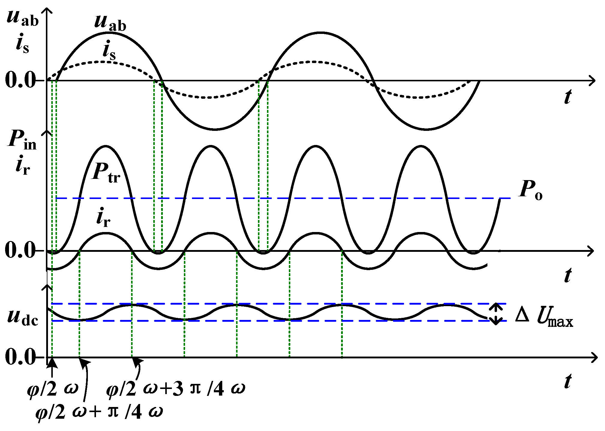
2. Power Analysis of a Single-Phase Rectifier

Figure 1 shows the typical topology of single-phase VSR. Part I and II are the H-bridge circuit and power decoupling loop, respectively. ir represents the second-order harmonic current of the line behind the H-bridge. irr is the input second-order ripple current of the power decoupling loop. The remaining second-order ripple current of the DC bus is represented by irc.
When the rectifier is operating at unit power factor, the AC input current is and the voltage us are kept in phase. In fact, a precise unit power factor is difficult to achieve; thus, there will be a small phase difference between is and us. In this case, the two can be expressed as follows:
u s = U s sin ω t ;
i s = I s sin ( ω t β ) ;
where Us and Is represent the amplitude of the input voltage and the input current, respectively. ω is the angular frequency of the grid voltage, and β is the phase of us leading is. From Equations (1) and (2), the input power Pin is:
P in = u s i s = U s I s 2 cos β U s I s 2 cos ( 2 ω t β ) .
According to Equation (2), the voltage drop uL on the inductor Ls is:
u L = L s d i s d t = ω L s I s cos ( ω t β ) .
From Equations (3) and (4), the power Ptr transmitted to the DC bus can be expressed as:
P tr = u s i s u L i s = U s I s 2 cos β ( U s I s 2 cos ( 2 ω t β ) + ω L I s 2 2 sin ( 2 ω t 2 β ) )
Equation (5) shows that Ptr consists of two parts: constant power Po and second-order ripple power Pr, which are expressed, respectively, as follows:
P o = U s I s 2 cos β ;
P r = ( U s I s 2 cos ( 2 ω t β ) + ω L I s 2 2 sin ( 2 ω t 2 β ) ) .
P0 is the output power of the rectifier. Pr is the second-order ripple power (i.e., the power to be processed in part II), which can be further expressed as follows:
P r = U s 2 I s 2 4 cos 2 β + ( ω L I s 2 2 U s I s 2 sin β ) 2 × sin ( 2 ω t 2 β + ψ )
ψ = arctan ( U s I s / 2 ) cos β ( ω L I s 2 / 2 ) ( U s I s / 2 ) sin β .
The above deduction shows that the phase angles β and ψ cannot be measured directly, which is not beneficial for controlling the power decoupling loop by the expression. To this end, the two phase angles are combined to establish a reference coordinate system with is as 0 phase, as shown in Figure 2. At this time, the calculation of the power Ptr transmitted to the DC bus is as follows:
P tr = u ab i s = U ab I s 2 cos φ U ab I s 2 cos ( 2 ω t φ ) .
In Equation (10), uab is the voltage of the ab bridge arm. φ is the phase of is ahead of uab. If the power decoupling circuit is not added, the second-order ripple power in the circuit is completely absorbed by the DC bus capacitors. As shown in Figure 2, the energy ΔE of the bus capacitor C filled in the period from φ/2ω to t is as follows:
Δ E = φ / 2 ω t U ab I s 2 cos ( 2 ω t φ ) d t = U ab I s 4 ω sin ( 2 ω t φ ) .
At the same time, the energy change of capacitor in this period ΔEc is as follows:
Δ E c = 1 2 C u dc 2 1 2 C U dc 2 ,
where udc is the DC bus voltage and Udc is its DC component. Ignoring the power loss in the circuit, Equations (11) and (12) should be equal; thus, the DC bus voltage is as follows:
u dc = U dc 2 U ab I s 2 ω C sin ( 2 ω t φ ) .
Applying Taylor’s formula to Equation (13), the results are approximately as follows:
u dc U dc U ab I s 4 ω C U dc sin ( 2 ω t φ ) .
From Equation (14), there is a second-order component in DC bus voltage. Refer to Equation (11) to calculate the capacitance C during φ/2ω +π/4ω to φ/2ω +3π/4ω period:
C = U a b I s 2 ω Δ U max U dc .
In Equation (15), ΔUmax is the maximum value of the DC bus voltage ripple. Considering the reliability of the power supply and normal operation of the equipment, the DC bus voltage ripple should be within the prescribed range, generally not more than 10%. If C is selected by Equation (15), a capacitor with larger capacitance value is needed to suppress the second-order ripple effectively. As a result, the buck-boost-type active power decoupling circuit is selected to absorb the second-order harmonic power on the DC side.

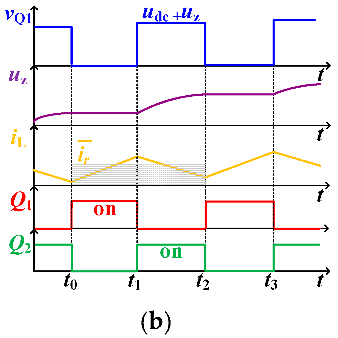
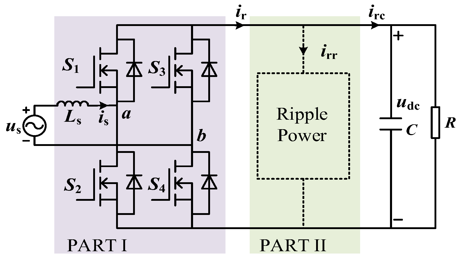
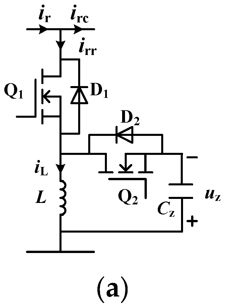
3. Analysis of an Active Power Decoupling Circuit

In this paper, a buck-boost-type power decoupling circuit is adopted [33]. Similarly, bidirectional buck-boost circuits can be used for power decoupling, such as the decoupling circuits in reference [27,32]. The characteristics of the three circuits are compared in Table 1, where d is the duty cycle of the bidirectional decoupling circuit. As shown in the table, the voltage stress and current stress of the buck-boost-type decoupling topology are not dominant. However, the choice of decoupling capacitance and capacitor voltage is more flexible, which will bring broad application prospects. Assuming that the second-order ripple power is constant, if the DC bus voltage is high, in order to avoid excessive voltage stress on the power device, a decoupling capacitor voltage lower than the DC bus voltage can be selected. From Equation (14), the ripple of the capacitor voltage is large at this time. In addition, if the voltage across the decoupling capacitor is high, the capacitance can be selected to be very small, thereby achieving an increase in power density. As a result, a buck-boost-type power decoupling circuit was selected in this paper.
The buck-boost-type power decoupling topology is shown in Figure 3a, in which capacitance acts as the energy storage element, while inductance acts as the energy transmission element. When the instantaneous power of the AC side is larger than that of DC side, that is, when the power decoupling circuit is in the charging mode (hereinafter referred to as charging mode), the switching modes of CCM are shown in Figure 3b. ir denotes the second-order ripple current processed in each switching cycle, iL denotes the instantaneous value of the inductor current in the decoupling loop, and vQ1 represents the voltage stress sustained by Q1. During t0t1 period, Q1 is on, and the pulsating power is transferred to the inductor. During the period from t1 to t2, Q1 is off, and the pulsating power flows through diode D2 to transfer energy to the capacitor.
Similarly, when the instantaneous power of the AC side is less than that of DC side, that is, when the power decoupling circuit is in discharging mode (hereinafter referred to as discharging mode), Q2 is on, and the pulsating power is transferred to the inductor. When Q2 is turned off, the pulsating power flows through the diode D1, and the energy is transmitted to the DC side.

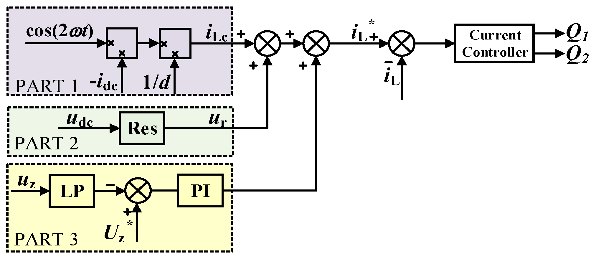
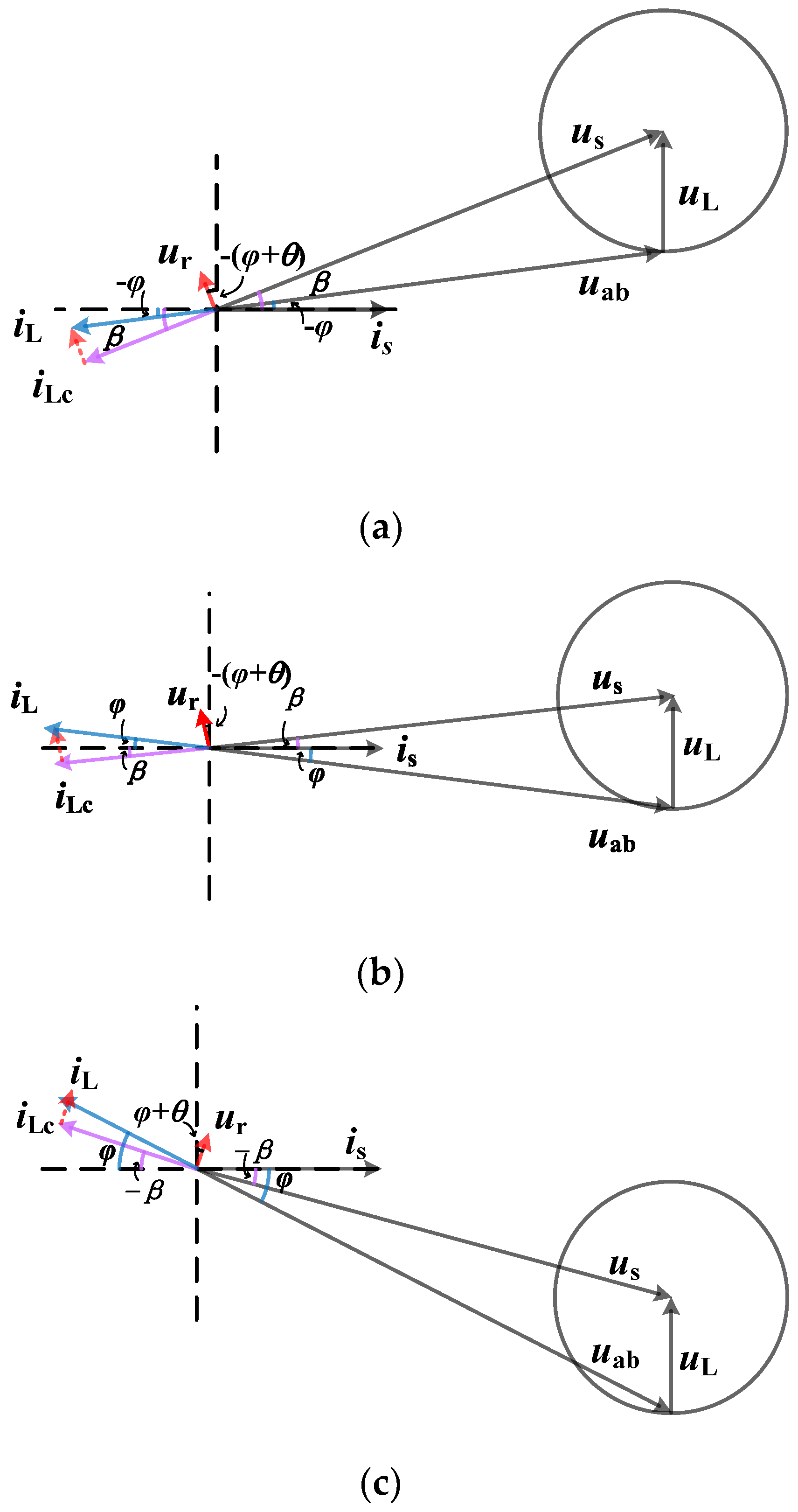
4. Control System Design

In order to eliminate the second-order ripple power on the DC bus, the precondition is to accurately obtain ir in Figure 1. If irr is controlled to equal ir, the DC bus voltage will be constant. Generally, there are two methods to obtain the second-order ripple current [32,33]. The first method is to sample ir directly and get its second-order component through the second-order resonant controller [33]. However, since the change of zero and nonzero values of pulsating current are consistent with the switching frequency, a higher sampling frequency is required. Only in this case can the signal be undistorted. It greatly increases the difficulty of the system’s hardware design. As a result, this paper selected the second method, which is to estimate ir by other variables in the circuit.
Ideally, the second-order ripple energy needs to be fully absorbed by the power decoupling circuit. According to Equation (10), the output power Ptro is as follows:
P tro = U ab I s 2 cos φ = U dc I dc ,
where Idc is the DC component of the load current on the DC side. The second-order harmonic power Ptrr is:
P trr = U ab I s 2 cos ( 2 ω t φ ) = U dc i r .
Combining Equations (16) and (17), ir is obtained as follows:
i r = I dc cos φ cos ( 2 ω t φ ) .
From Figure 3, the second-order ripple current iL on the inductor of the decoupling circuit is:
i L = 1 d i r ,
where d is the duty cycle of Q1 in the buck-boost circuit. According to the control method in [30,31], the command value iLc is set to:
i Lc = I dc d cos ( 2 ω t + β ) .
The duty cycle d in Equation (20) is calculated by the DC component of DC bus voltage udc and decoupling capacitor voltage uz. Figure 4 shows the control block diagram of the power decoupling circuit. From Equation (20), part 1 in Figure 4 can be obtained. This command value is only an approximation of ir. Since the phase difference φ is ignored, there is a deviation between the command value iLc and the actual value iL. To this end, this paper introduced DC bus voltage udc to participate in the estimation of ir.
The function of DC bus voltage in the power decoupling circuit is shown in part 2 in Figure 4. Res represents the second-order resonant controller, which extracts the second-order component of udc (i.e., ur). Because most of the second-order ripple energy in the circuit is absorbed by the power decoupling circuit, according to Equation (14), the second-order ripple component of the DC bus voltage can be expressed as:
u r = E sin ( 2 ω t φ ) .
Referring to Equations (11) and (14), E´ represents a value proportional to the second-order ripple energy of the DC bus. It is a constant to characterize ur. Equation (21) is based on the fact that the second-order ripple component of the DC side is completely absorbed by the DC bus capacitor (i.e., the ripple current does not flow through the output). In fact, this condition is only valid when the DC bus capacitance is large enough. However, after the power decoupling circuit is added, the DC bus capacitance decreases, and the second-order ripple component also exists in the load current. At this time, the second-order component of the DC bus voltage should be expressed as:
u r = E sin ( 2 ω t φ θ ) .
Equation (22) shows that the DC bus capacitor is also considered as the load, and θ is the impedance angle of the RC load. Expressing the command values iLc and ur by phasors gives:
i Lc + u r = I d c d ( β + π ) + E ( π / 2 φ θ ) .
Equation (23) can be rewritten as:
i Lc + u r = M Q ;
M = ( I d c cos β d E sin ( φ + θ ) ) 2 + ( E cos ( φ + θ ) d I d c sin β ) 2 ;
Q = π / 2 + arctan I dc cos β d E sin ( φ + θ ) d E cos ( φ + θ ) I dc sin β .
Plotting the phasor form of the above variables in a vector diagram is shown in Figure 5. The figure will present the function of udc in the control circuit more intuitively. There is a phase difference between the command value iLc and the actual inductor current iL. Since the output amplitude of ur is small, if ur is superimposed on iLc, the estimated command value of the second-order current is basically unchanged. Moreover, the superimposed phase approaches the phase of ir. As a result, the control of the second-order ripple absorption is more accurate.
At the same time, this method is highly applicable because the phase can be compensated in four quadrants. The phasors in the first and second quadrants are shown in Figure 5. The same applies to the third and fourth quadrants.
Part 3 in Figure 4 shows the control of uz. LP represents the low-pass filter, which extracts the DC component of uz. The superposition of part 1, part 2, and part 3 serves as the given value of iL.

5. Parameter Design

5.1. Inductance Design of the Power Decoupling Circuit

The inductance of the power decoupling circuit was designed in CCM. In charging mode, the following can be seen from Figure 3b:
When Q1 is on, the inductor charges:
K 1 = u dc L ,
where K1 indicates the rise rate of the inductor current during charging. When Q1 is off, the inductor discharges:
K 2 = u z L ,
where K2 represents the drop rate of the inductor current during discharging. In this process, the second-order ripple energy is transferred to the inductor and then to the capacitor.
Ignoring the energy storage on the inductor in a switching period, that is, the second-order ripple energy injected into the inductor is approximately equal to the average value of second-order ripple energy processed by decoupling loop in a switching period:
i r T 1 2 K 1 T 1 2 ,
where T1 indicates the time when Q1 is turned on in one switching cycle, and T represents one switching period. Combining Equations (27) and (28) with (29), the duty cycle dc of Q1 is:
d c 2 i r f r L u dc ,
where fr is the switching frequency of power decoupling circuit, which is equal to the switching frequency of rectifier circuit in this paper. Similarly, in a switching cycle, the second-order ripple energy flowing from the inductor is approximately equal to the average value of second-order ripple energy processed by the decoupling loop. As a result, the duty cycle dd of Q2 is:
d d 2 i r f r L u dc u z .
At the peak current of the inductor, the current ripple is the largest. Thus, the peak current value of the inductor is taken to calculate the minimum value of the required inductance. From Equation (20), the peak value iLmax of the inductor current is approximately as follows:
i L max = I dc d .
Since the current only plays the role of energy transmission, the ripple index is not strictly required; therefore, the ripple is calculated by 1.5 times.
According to the given ripple index, when Q1 is on or off, L must be met respectively:
u dc L d c T 2 i L max 1.5 ;
u z L d d T 2 i Lmax 1.5 .
The range of L is obtained as follows:
L 2 u dc u z 2 9 I dc f r ( u dc + u z ) 2 = L 1 .
Moreover, the peak current ripple value of the inductor should be less than the maximum value Ip allowed to flow through the inductor. When the average current value of the inductor reaches iLmax in a switching cycle, L is calculated as follows:
i Lmax + U dc 2 L d c T I p ;
i L max + U z 2 L d d T I p .
The range of L is obtained as follows:
L u dc i r 2 f r ( I p i L max ) 2 = L 2 .
The calculation of inductance selection in discharging mode is the same. By Equations (27)–(38), the selection of inductance should follow:
L > ( L 1 L 2 ) .
That is, the selected inductance L should be greater than the maximum values of L1 and L2.

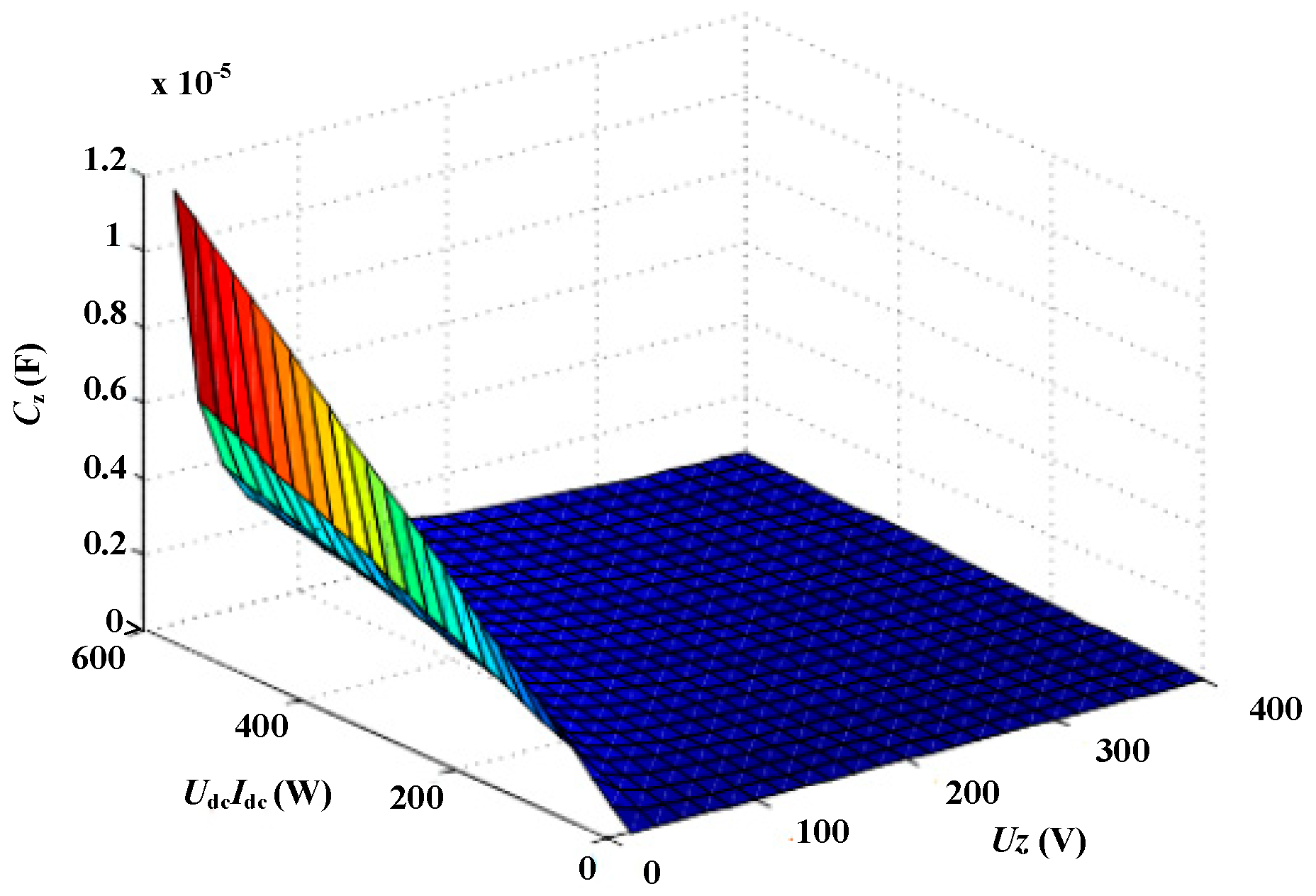
5.2. Capacitance Design of the Power Decoupling Circuit

From Equation (15), the selection of capacitance in the decoupling circuit is related to the average value and the ripple of decoupling capacitor voltage. Therefore, the maximum value of capacitor voltage ripple ΔUzmax is obtained:
Δ U zmax = U ab I s 2 ω C z u z ,
In order to ensure the continuity of capacitor voltage and normal operation of the decoupling circuit, the following conditions should be satisfied:
Δ U zmax 2 u z .
A combination of Equations (40) and (41) can be further expressed as:
U dc I dc 2 ω C z u z 2 .
The relationship of capacitance, capacitor voltage. and output power is plotted in Figure 6 based on Equation (42). From the figure, if the capacitance Cz is larger, the capacitor voltage uz can be made smaller; thus, the voltage stress of the decoupling loop can be reduced. If uz is higher, Cz can be reduced accordingly. If the output power increases, Cz needs to increase to maintain effective operation.

6. Simulation and Experiment

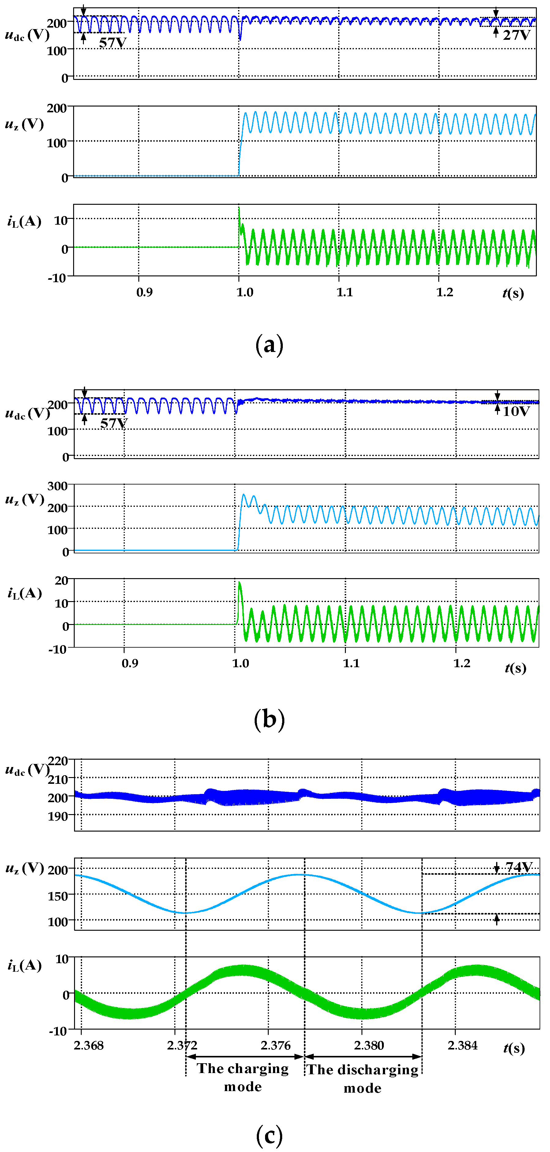
6.1. Simulation Verification

In order to verify the feasibility of the control method, two sets of simulation models were built for comparison. The first group adopted the control method in [30,31]. This method estimated ir without phase compensation, and the power decoupling circuit was in CCM, which is called the estimation method for short. The second group adopted the control method proposed in this paper. The two sets of control methods were based on the same rectifier and power decoupling topology. Their simulation parameters are shown in Table 2.
The steady-state simulation waveforms of the estimation method and the proposed method are compared. Under the estimation method, the simulation waveforms before and after the power decoupling loop was connected are shown in Figure 7a. Before 1 s, the power decoupling circuit was not connected. At this time, the second-order ripple energy in the system was all processed by the DC bus capacitor. From the figure, the peak-to-peak value of the voltage ripple reached 57 V, the capacitor voltage and inductor current in the decoupling circuit were both 0 V. After the power decoupling circuit was connected at 1 s, the circuit gradually restored to steady state. The fluctuation of DC bus voltage was greatly reduced compared with that before 1 s, but the DC bus voltage still had a ripple of 27 V.
Under the proposed method, the simulation waveforms before and after the power decoupling circuit was connected are shown in Figure 7b. The power decoupling circuit was also connected at 1 s. After the system was stable, the DC bus voltage ripple was 10 V, which was 17 V less than that in the estimation method. It can be seen that the DC bus voltage ripple was smaller, and the second-order ripple power processing was more effective by the proposed method. Although 150 μF capacitance was introduced into the circuit, if the power decoupling circuit was not connected, a DC bus capacitance C of 1400 μF was needed to achieve the same effect. The waveforms of the power decoupling circuit in two ripple periods are shown in Figure 7c. The average voltage of the decoupling capacitor Cz was stable at 150 V; the voltage ripple was 74 V. In the charging mode, the average value of the inductor current was greater than 0 in each switching cycle; thus, the capacitor voltage uz rose. The waveform in the discharging mode was similar. The control method was validated by simulation.

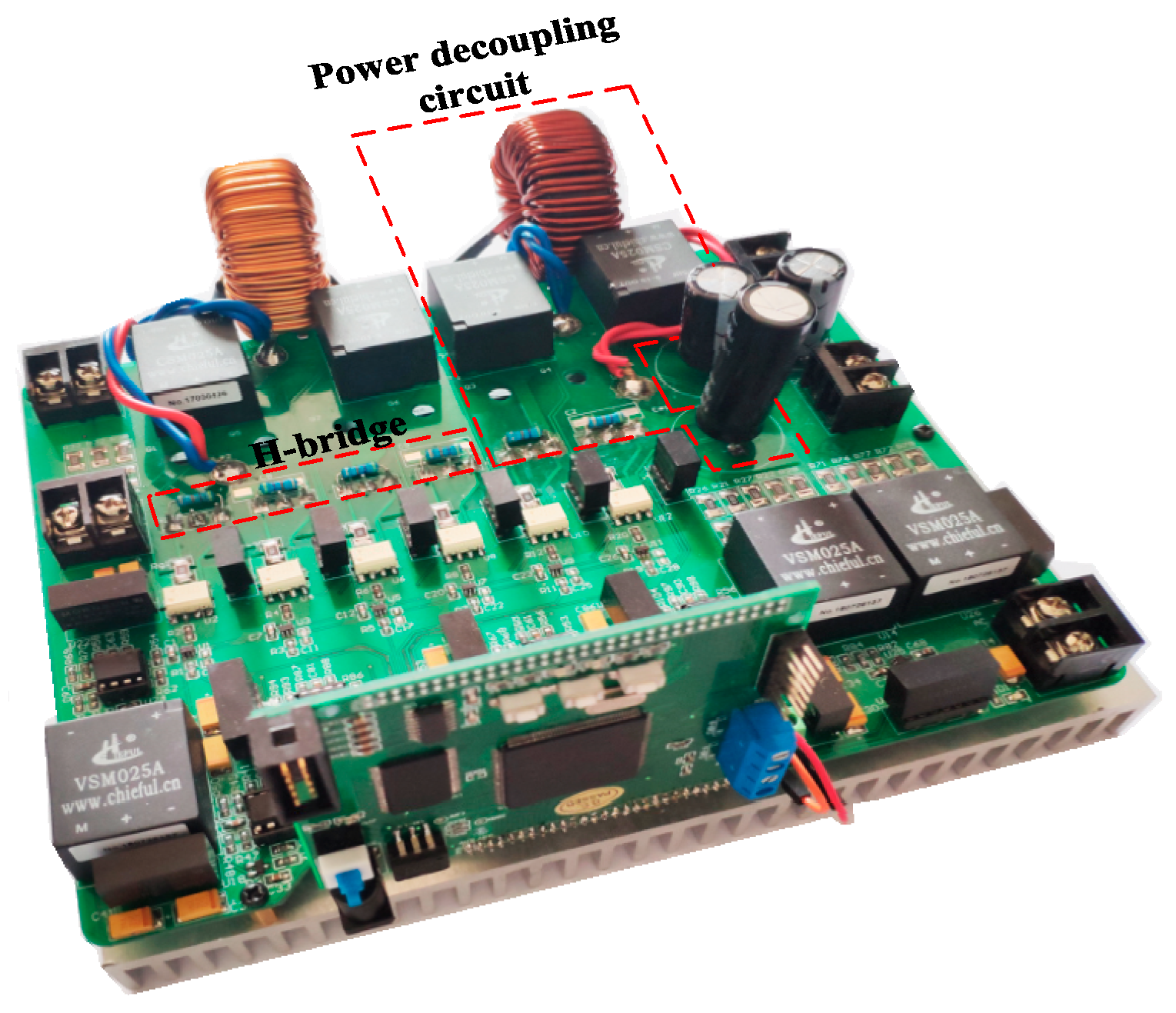
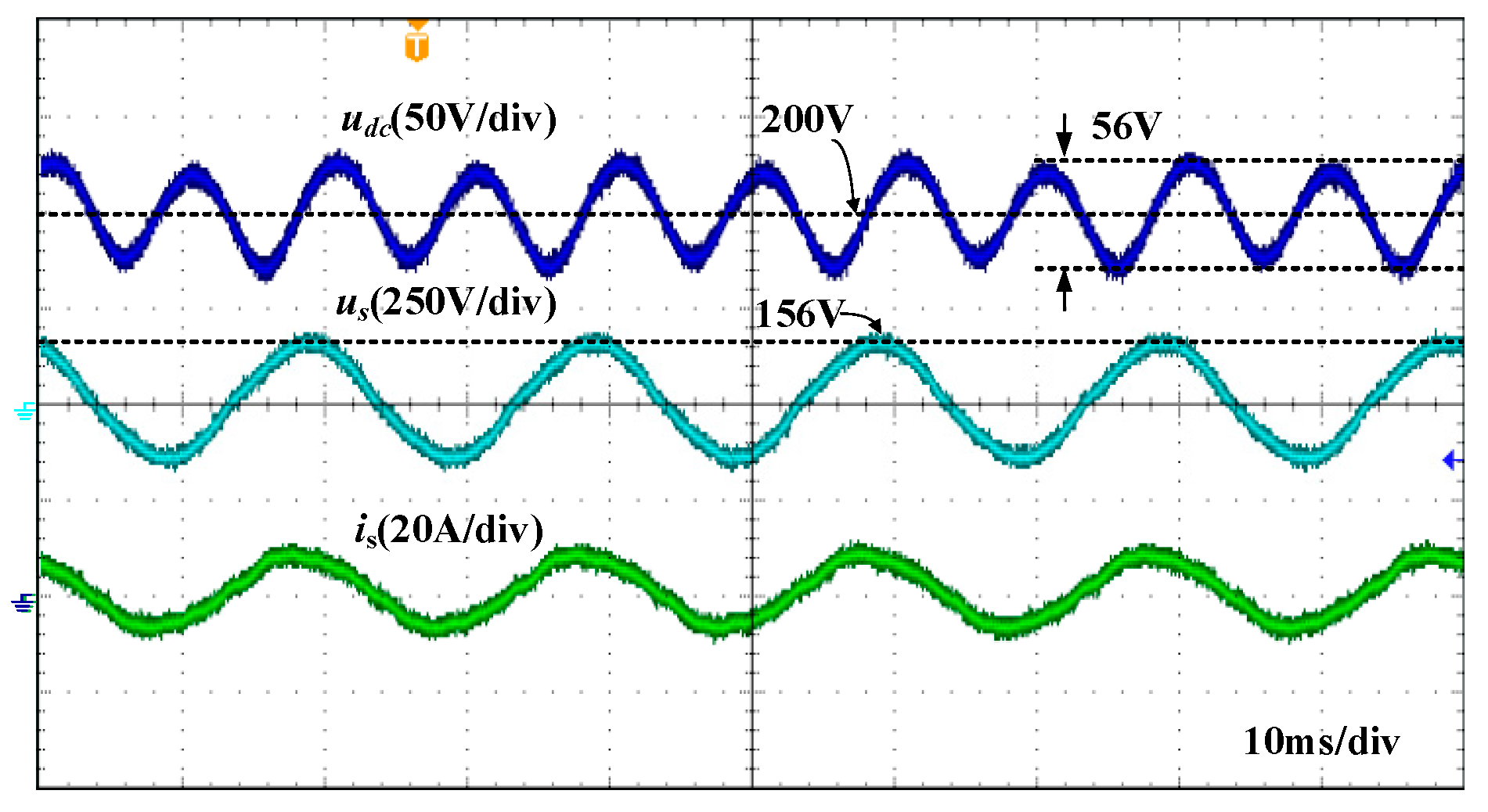
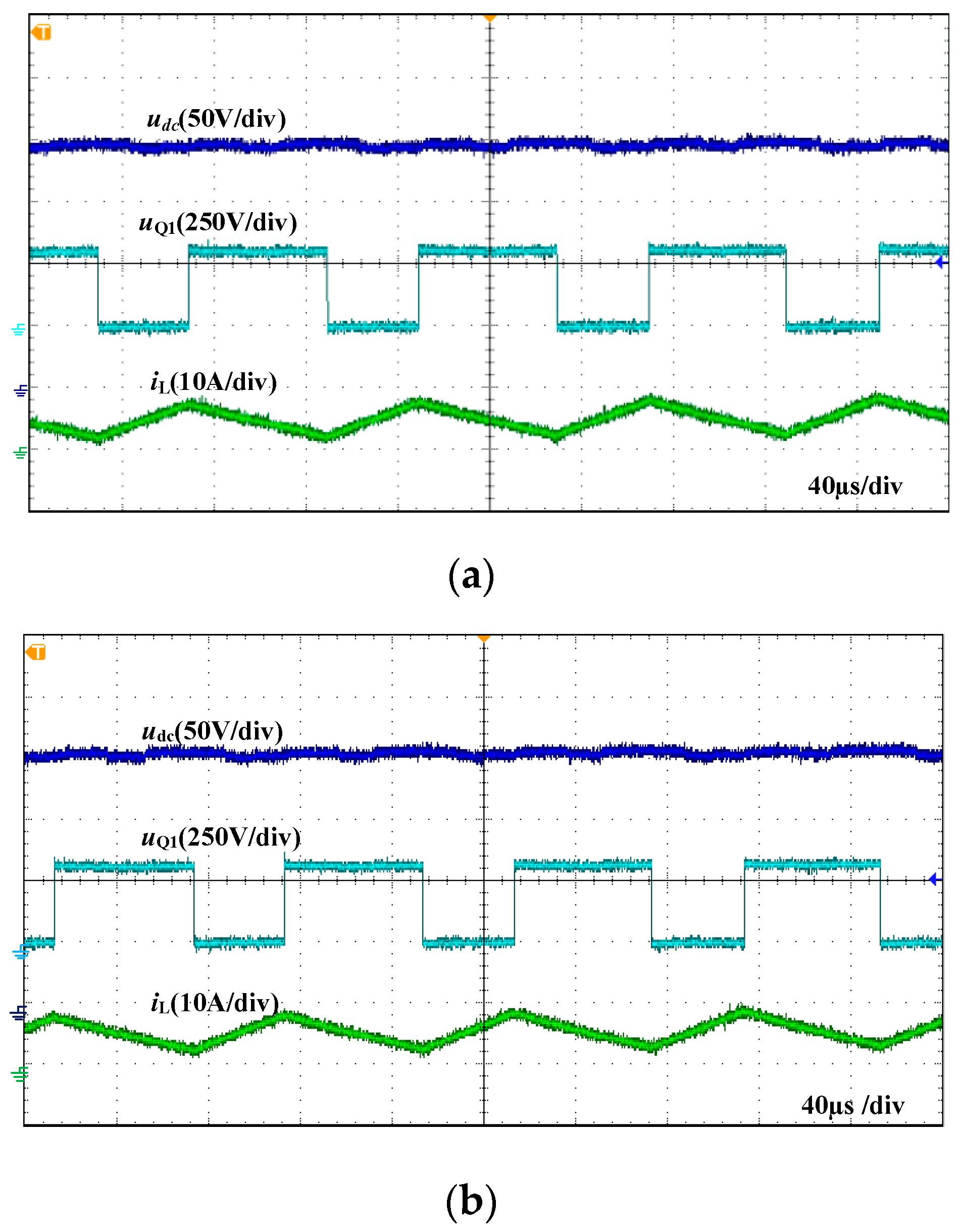
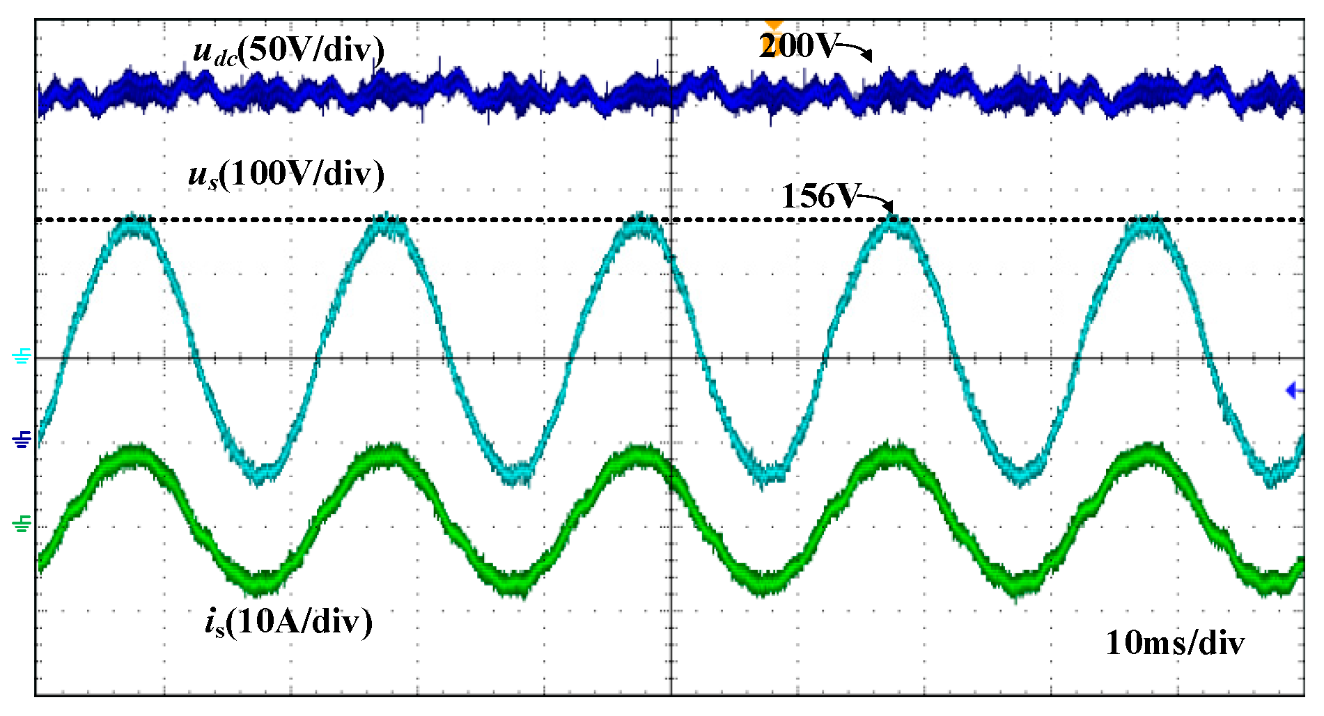
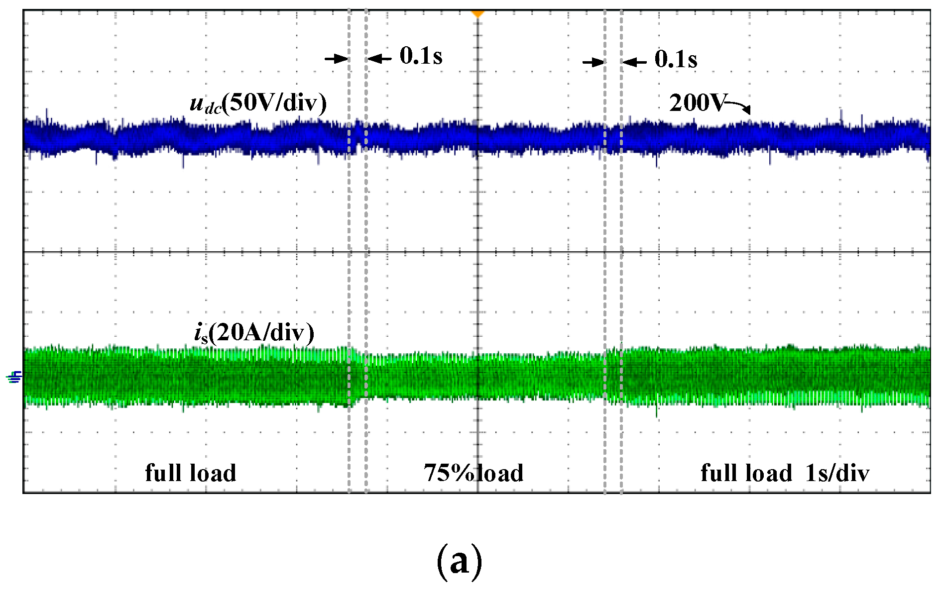
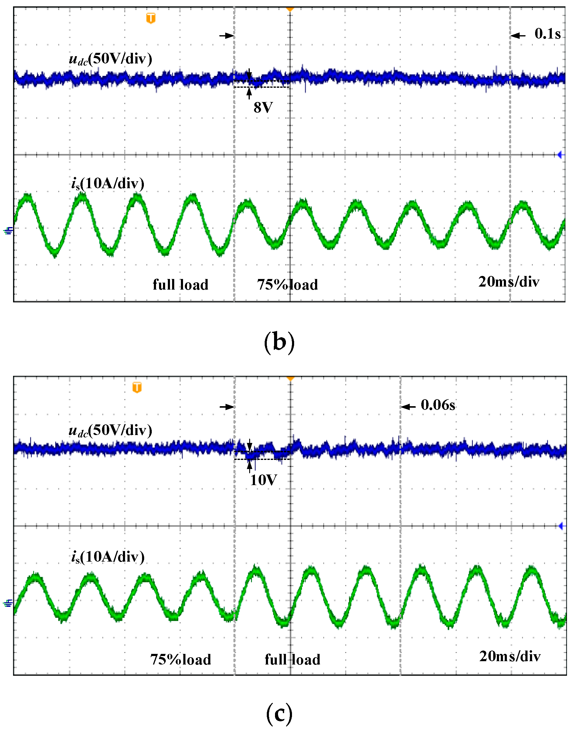
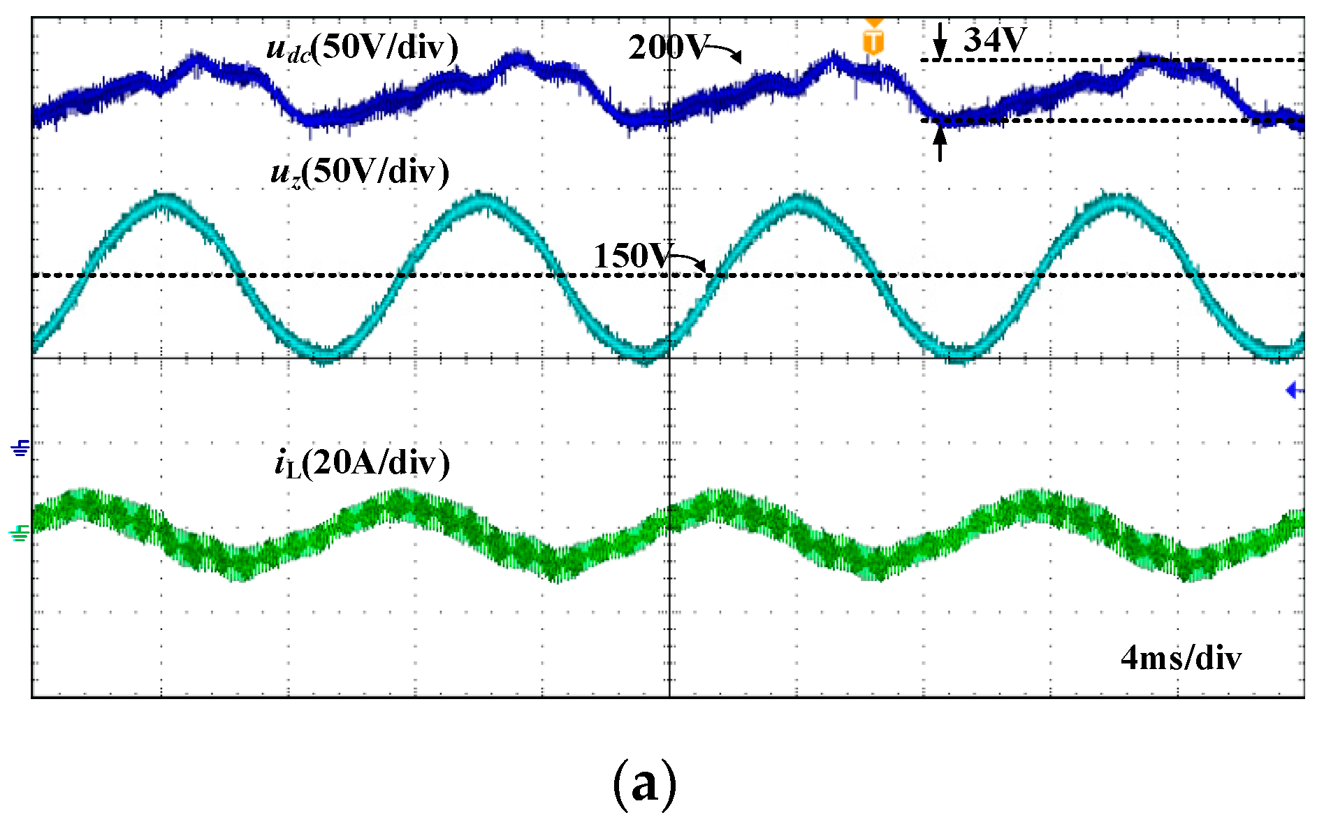
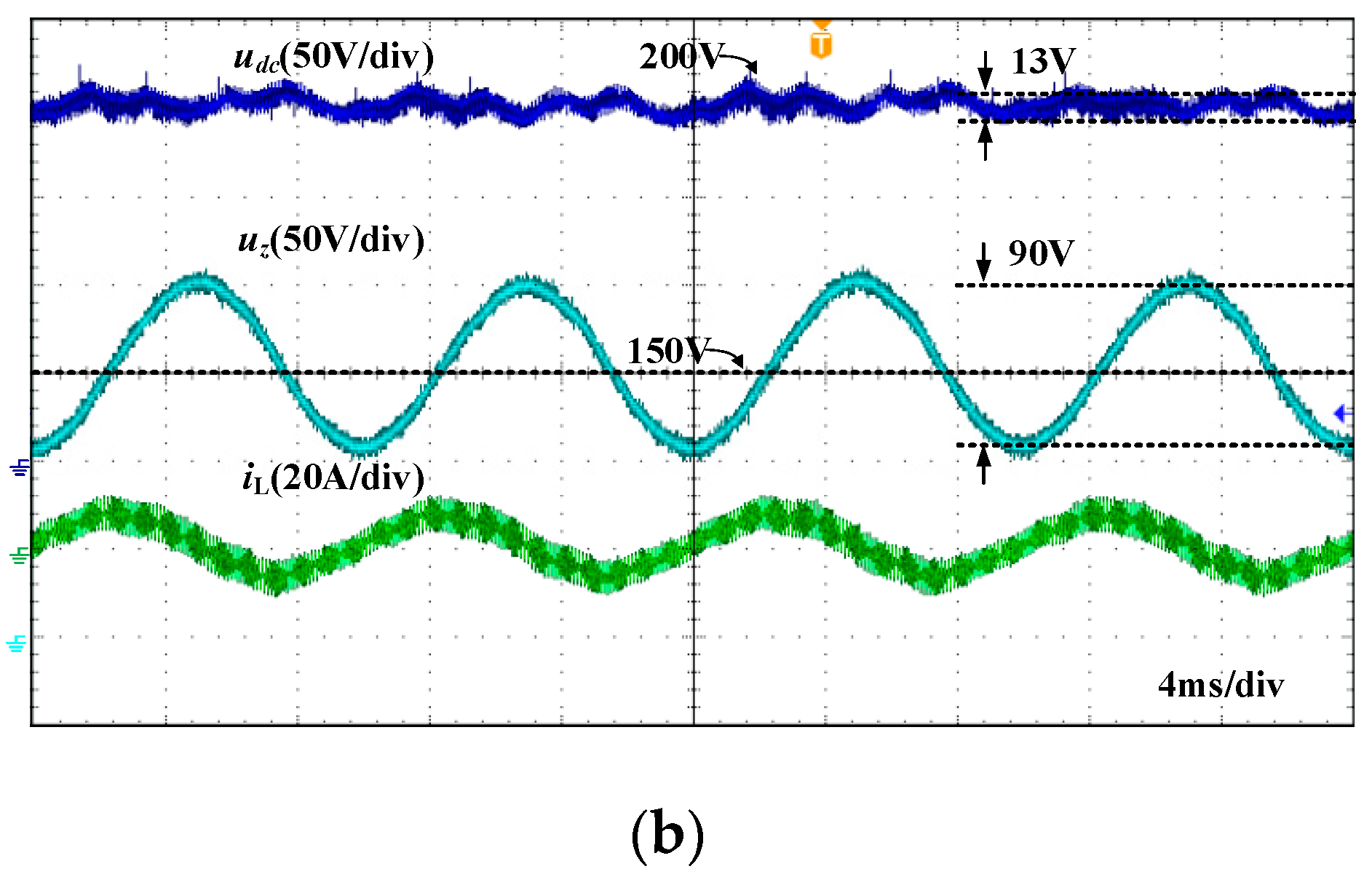
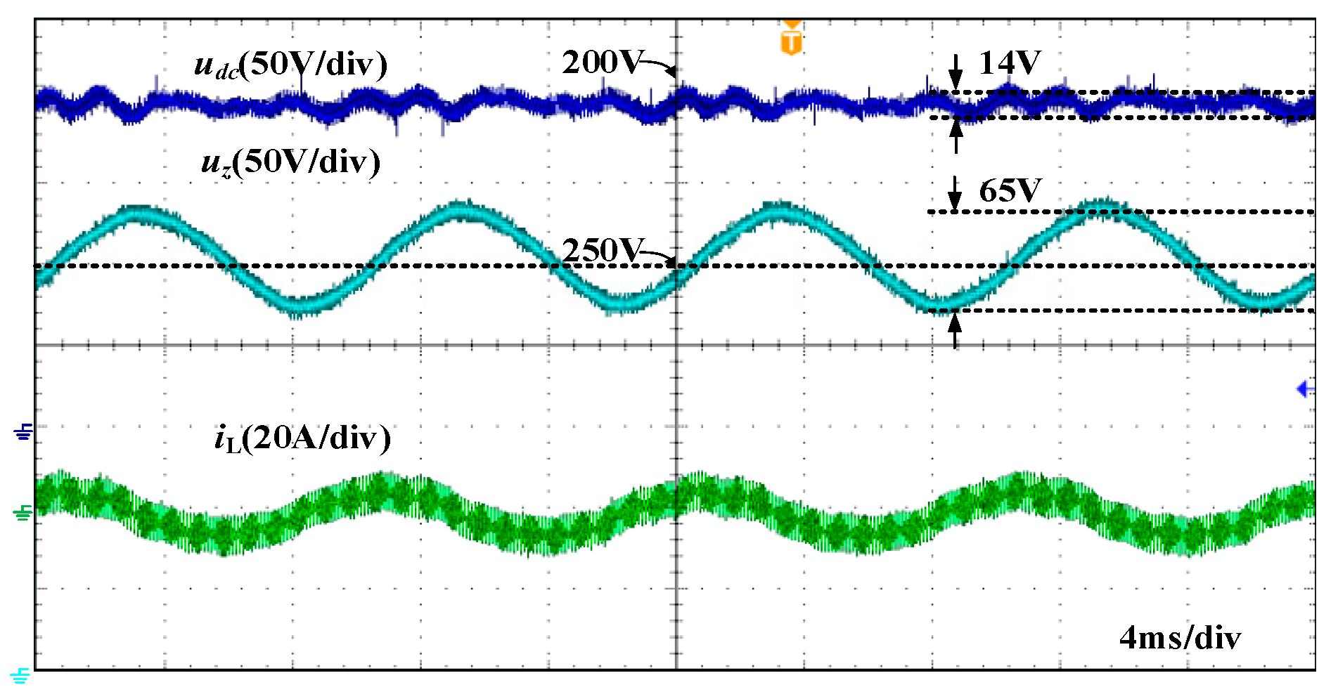
6.2. Experiment Verification

Similar to simulations, two groups of experiments were carried out based on the same experimental prototype. Figure 8 is a picture of the prototype, the parameters of which are selected as in Table 2. The experiment waveforms without a power decoupling circuit are shown in Figure 9. When the power decoupling loop was not connected, the DC bus capacitor was selected to be 250 μF, which is the sum of the DC bus capacitor C and the decoupling capacitor Cz in Table 2. As the figure shows, the voltage and current were in phase, but the voltage fluctuated greatly, and the ripple reached 56 V. A large harmonic component was introduced into the AC input current; thus, the inductor’s current waveform was not ideal.
When the power decoupling circuit was connected, the experiment waveforms obtained by the estimation method and the proposed method are shown in Figure 10. The average voltage of the decoupling capacitor Cz was 150 V. As shown in Figure 10a, the voltage ripple obtained by the estimation method was 34 V, which was 11% less than that without the power decoupling loop. Eleven percent represents the ripple ratio of the DC bus voltage; it was derived from the formula: ΔUmax/Udc*×100%. It was proved that this method was effective for second-order ripple power absorption, but the calculation was not accurate enough; thus, the second-order ripple content of the DC bus voltage was still large. As shown in Figure 10b, the voltage ripple of the bus obtained by the proposed method was 13 V within the prescribed range of 10%, which was 20% less than that without the power decoupling loop. Thus, the validity of the proposed control method was verified. The capacitor voltage ripple of the decoupling loop was 90 V, and the inductor current presented a second-order sinusoidal curve with a peak value approximating 6.2 A, which was basically consistent with the simulation results.
Experiment waveforms of the ripple of iL and the ripple of udc in each switching cycle are shown in Figure 11. Because of the time axis of the oscilloscope, udc was approximately constant over the field of view. L was charged and discharged in each switching cycle with the opening and closing of Q1.
At this time, the operation of the whole system is observed. The experiment waveforms of the input voltage, input current, and output voltage are shown in Figure 12 by the proposed method. As shown in the figure, the input voltage and current were approximately in phase. The input current had a higher sinusoidal degree and a lower harmonic content, which was notably better than that without power decoupling, as shown in Figure 9. As a result, the goal of power decoupling is achieved.
Taking full advantage of the buck-boost circuit’s step-up and step-down advantages, the capacitor voltage uz of the decoupling circuit can be controlled to be higher than that of the DC bus, with an average value of 250 V instead of the average value of 150 V above. Figure 13 shows the experiment waveforms of the proposed method under this voltage level. As shown in the figure, the bus voltage ripple was 14 V within the prescribed range of 10%. The capacitor voltage ripple of the decoupling circuit was 65 V, which is smaller than that when the average value of uz was 150 V. Therefore, under the condition of maintaining the same DC bus voltage ripple, if the capacitor voltage uz of the decoupling loop is increased, the voltage ripple will be reduced. The capacitance Cz can be taken to a smaller value accordingly.
In order to verify the good dynamic characteristics of the system, a load switching experiment was carried out. Figure 14a shows the experiment waveforms when the full load was switched to 75% load and then switched to full load. The 75 % load indicated that the output power was 75% of the rated power. Figure 14b,c shows the experiment waveforms in load reduction and load increase, respectively. It can be seen that the rise and fall of voltage did not exceed 10 V, and the response time was short. Within 0.1 s after load switching, the system reached steady-state quickly, indicating that the system has good dynamic performance during load switching.

7. Conclusions

Based on buck-boost-type power decoupling circuit of the single-phase VSR, an independent power decoupling control strategy with second-order ripple current estimation was proposed in this paper. The second-order ripple component of the DC bus voltage was introduced in the control, which compensated the phase deviation between the command value and the actual value of the second-order ripple current. Thus, the power decoupling circuit can effectively absorb the second-order ripple power, and the DC bus voltage ripple is controlled within the allowable range. Finally, an experimental prototype of 533 W rated power was built for the experiment. With the proposed control method, the DC bus voltage ripple was controlled within 7% in steady state, the voltage overshoot was not more than 10 V in load switching, and the transition time was not more than 0.2 s, which verifies the effectiveness of the control method with a good dynamic response and stable characteristics.

Author Contributions

Conceptualization, M.Q.; Formal analysis, M.Q.; Investigation, M.Q., H.B., and Z.W.; Methodology, M.Q. and P.W.; Project administration, P.W.; Software, M.Q., H.B., and Z.W.; Supervision, P.W.; Validation, P.W.; Writing—original draft, M.Q.; Writing—review & editing, M.Q., P.W., H.B., and Z.W.

Funding

This research received no external funding.

Acknowledgments

This work is sponsored by The Basic Research Project of Qinghai Province, China (Year 2018) No.2018-ZJ-764. (Research on Control Strategy of Long-Distance Consumption of Distributed PV Stations via HVDC).

Conflicts of Interest

The authors declare no conflict of interest.

References

  1. Alves, W.C.; Morais, L.M.F.; Cortizo, P.C. Design of an Highly Efficient AC-DC-AC Three-Phase Converter Using SiC for UPS Applications. Electronics 2018, 7, 425. [Google Scholar] [CrossRef]
  2. Monteiro, V.; Afonso, J.A.; Ferreira, J.C.; Afonso, J.L. Vehicle Electrification: New Challenges and Opportunities for Smart Grids. Energies 2019, 12, 118. [Google Scholar] [CrossRef]
  3. Nguyen, M.-K.; Choi, Y.-O. Voltage Multiplier Cell-Based Quasi-Switched Boost Inverter with Low Input Current Ripple. Electronics 2019, 8, 227. [Google Scholar] [CrossRef]
  4. Nicolas-Apruzzese, J.; Lupon, E.; Busquets-Monge, S.; Conesa, A.; Bordonau, J.; García-Rojas, G. FPGA-Based Controller for a Permanent-Magnet Synchronous Motor Drive Based on a Four-Level Active-Clamped DC-AC Converter. Energies 2018, 11, 2639. [Google Scholar] [CrossRef]
  5. Pan, H.; Ding, M.; Bi, R.; Sun, L. Research on Cooperative Planning of Distributed Generation Access to AC/DC Distribution (Micro) Grids Based on Analytical Target Cascading. Energies 2019, 12, 1847. [Google Scholar] [CrossRef]
  6. Zeb, K.; Islam, S.U.; Din, W.U.; Khan, I.; Ishfaq, M.; Busarello, T.D.C.; Ahmad, I.; Kim, H.J. Design of Fuzzy-PI and Fuzzy-Sliding Mode Controllers for Single-Phase Two-Stages Grid-Connected Transformerless Photovoltaic Inverter. Electronics 2019, 8, 520. [Google Scholar] [CrossRef]
  7. Li, B.; Huang, S.; Chen, X. Performance Improvement for Two-Stage Single-Phase Grid-Connected Converters Using a Fast DC Bus Control Scheme and a Novel Synchronous Frame Current Controller. Energies 2017, 10, 389. [Google Scholar] [CrossRef]
  8. Zhang, J.; Ding, H.; Wang, B.; Guo, X.; Padmanaban, S. Active Power Decoupling for Current Source Converters: An Overview Scenario. Electronics 2019, 8, 197. [Google Scholar] [CrossRef]
  9. Li, B.; Zhou, L. Power Decoupling Method Based on the Diagonal Compensating Matrix for VSG-Controlled Parallel Inverters in the Microgrid. Energies 2017, 10, 2159. [Google Scholar] [Green Version]
  10. Hong, J.; Vilathgamuwa, M.; Yin, J.; Liu, Y.; Peng, J.; Jiang, H. Power Decoupling of a Single Phase DC-AC Dual Active Bridge Converter Based on an Integrated Bidirectional Buck/Boost Stage. Energies 2018, 11, 2746. [Google Scholar] [CrossRef]
  11. Ertasgin, G.; Whaley, D.M.; Ertugrul, N.; Soong, W.L. Analysis of DC Link Energy Storage for Single-Phase Grid-Connected PV Inverters. Electronics 2019, 8, 601. [Google Scholar] [CrossRef]
  12. Lu, N.; Yang, S.; Tang, Y. Ripple Current Reduction for Fuel Cell Powered Single-Phase Uninterruptible Power Supplies. IEEE Trans. Ind. Electron. 2017, 64, 6607–6617. [Google Scholar] [CrossRef]
  13. Yang, Y.; Zhou, K.; Wang, H.; Blaabjerg, F. Analysis and Mitigation of Dead-Time Harmonics in the Single-Phase Full-Bridge PWM Converter with Repetitive Controllers. IEEE Trans. Ind. Appl. 2018, 54, 5343–5354. [Google Scholar] [CrossRef]
  14. Mozaffari, K.; Amirabadi, M.; Deshpande, Y. A Single-Phase Inverter/Rectifier Topology with Suppressed Double-Frequency Ripple. IEEE Trans. Power Electron. 2018, 33, 9282–9295. [Google Scholar] [CrossRef]
  15. Liu, Y.; Sun, Y.; Su, M.; Zhou, M.; Zhu, Q.; Li, X. A Single-Phase PFC Rectifier with Wide Output Voltage and Low-Frequency Ripple Power Decoupling. IEEE Trans. Power Electron. 2018, 33, 5076–5086. [Google Scholar] [CrossRef]
  16. Huang, K.; Wang, Y.; Wai, R. Design of Power Decoupling Strategy for Single-Phase Grid-Connected Inverter Under Nonideal Power Grid. IEEE Trans. Power Electron. 2019, 34, 2938–2955. [Google Scholar] [CrossRef]
  17. Sun, Y.; Liu, Y.; Su, M.; Xiong, W.; Yang, J. Review of Active Power Decoupling Topologies in Single-Phase Systems. IEEE Trans. Power Electron. 2016, 31, 4778–4794. [Google Scholar] [CrossRef]
  18. Hu, H.; Harb, S.; Kutkut, N.; Batarseh, I.; Shen, Z.J. A Review of Power Decoupling Techniques for Microinverters with Three Different Decoupling Capacitor Locations in PV Systems. IEEE Trans. Power Electron. 2013, 28, 2711–2726. [Google Scholar] [CrossRef]
  19. Li, W.; Gu, Y.; Luo, H.; Cui, W.; He, X.; Xia, C. Topology Review and Derivation Methodology of Single-Phase Transformerless Photovoltaic Inverters for Leakage Current Suppression. IEEE Trans. Ind. Electron. 2015, 62, 4537–4551. [Google Scholar] [CrossRef]
  20. Sun, H.; Wang, H.; Qi, W. Automatic Power Decoupling Controller of Dependent Power Decoupling Circuit for Enhanced Transient Performance. IEEE Trans. Ind. Electron. 2019, 66, 1820–1831. [Google Scholar] [CrossRef]
  21. Li, S.; Qi, W.; Tan, S.; Hui, S.Y. Integration of an Active Filter and a Single-Phase AC/DC Converter with Reduced Capacitance Requirement and Component Count. IEEE Trans. Power Electron. 2016, 31, 4121–4137. [Google Scholar] [CrossRef]
  22. Watanabe, H.; Sakuraba, T.; Furukawa, K.; Kusaka, K.; Itoh, J. Development of DC to Single-Phase AC Voltage Source Inverter with Active Power Decoupling Based on Flying Capacitor DC/DC Converter. IEEE Trans. Power Electron. 2018, 33, 4992–5004. [Google Scholar] [CrossRef]
  23. Jamatia, A.; Gautam, V.; Sensarma, P. Power Decoupling for Single-Phase PV System Using Æuk Derived Microinverter. IEEE Trans. Ind. Appl. 2018, 54, 3586–3595. [Google Scholar] [CrossRef]
  24. Zhu, G.; Wang, H.; Liang, B.; Tan, S.; Jiang, J. Enhanced Single-Phase Full-Bridge Inverter with Minimal Low-Frequency Current Ripple. IEEE Trans. Ind. Electron. 2016, 63, 937–943. [Google Scholar] [CrossRef]
  25. Yao, W.; Loh, P.C.; Tang, Y.; Wang, X.; Zhang, X.; Blaabjerg, F. A Robust DC-Split-Capacitor Power Decoupling Scheme for Single-Phase Converter. IEEE Trans. Power Electron. 2017, 32, 8419–8433. [Google Scholar] [CrossRef]
  26. Xu, S.; Shao, R.; Chang, L.; Mao, M. Single-Phase Differential Buck–Boost Inverter with Pulse Energy Modulation and Power Decoupling Control. IEEE J. Sel. Topics Power Electron. 2018, 6, 2060–2072. [Google Scholar] [CrossRef]
  27. Zhong, Q.C.; Ming, W.L.; Cao, X.; Krstic, M. Control of Ripple Eliminators to Improve the Power Quality of DC Systems and Reduce the Usage of Electrolytic Capacitors. IEEE Access. 2016, 4, 2177–2187. [Google Scholar] [CrossRef]
  28. Xiao, S.; Li, X.; Zhang, H.; Balog, R.S. Active power decoupling method based on dual buck circuit with model predictive control. In Proceedings of the 2018 IEEE Applied Power Electronics Conference and Exposition (APEC), San Antonio, TX, USA, 4–8 March 2018; pp. 3089–3094. [Google Scholar]
  29. Li, X.; Xiao, S.; Zhang, H.; Balog, R.S.; Ge, B. Dual buck based power decoupling circuit for single phase inverter/rectifier. In Proceedings of the 2016 IEEE Energy Conversion Congress and Exposition (ECCE), Milwaukee, WI, USA, 18–22 September 2016; pp. 1–6. [Google Scholar]
  30. Chao, K.; Cheng, P. Power decoupling methods for single-phase three-poles AC/DC converters. In Proceedings of the 2009 IEEE Energy Conversion Congress and Exposition (ECCE), San Jose, CA, USA, 20–24 September 2009; pp. 3742–3747. [Google Scholar]
  31. Itoh, J.I.; Watanabe, H.; Koiwa, K.; Ohnuma, Y. Experimental verification of single-phase inverter with power decoupling function using boost-up chopper. In Proceedings of the 2013 15th European Conference on Power Electronics and Applications (EPE), Lille, France, 3–5 September 2013; pp. 1–10. [Google Scholar]
  32. Wang, R.; Wang, F.; Boroyevich, D.; Burgos, R.; Lai, R.; Ning, P. A High Power Density Single Phase PWM Rectifier with Active Ripple Energy Storage. IEEE Trans. Power Electron. 2011, 26, 1430–1443. [Google Scholar] [CrossRef]
  33. Cao, X.; Zhong, Q.; Ming, W. Ripple Eliminator to Smooth DC-Bus Voltage and Reduce the Total Capacitance Required. IEEE Trans. Ind. Electron. 2015, 62, 2224–2235. [Google Scholar] [CrossRef]
Figure 1. Topology of single-phase VSR with a power decoupling circuit.
Electronics 08 00841 g001
Figure 2. Waveforms of different variables in the system.
Electronics 08 00841 g002
Figure 3. The buck-boost-type power decoupling circuit and the modal diagram in continuous current mode (CCM): (a) the buck-boost-type power decoupling topology; (b) the modal diagram in CCM.
Electronics 08 00841 g003aElectronics 08 00841 g003b
Figure 4. Control block diagram of the power decoupling circuit.
Electronics 08 00841 g004
Figure 5. Phasor diagram of different variables in the rectifier: (a) Case 1 in quadrant I, the angle between uL and uab is acute; (b) Case 2 in quadrant I, the angle between uL and uab is obtuse; and (c) Quadrant II.
Electronics 08 00841 g005
Figure 6. Selection range of capacitance in the power decoupling circuit.
Electronics 08 00841 g006
Figure 7. Comparison of steady-state simulation waveforms of the estimation method and the proposed method: (a) the estimation method; (b) the proposed method; and (c) the proposed method in two ripple periods.
Electronics 08 00841 g007
Figure 8. Picture of the experiment prototype.
Electronics 08 00841 g008
Figure 9. Experiment waveforms of input voltage us, input current is, and output voltage udc without the power decoupling circuit.
Electronics 08 00841 g009
Figure 10. Experiment waveforms of the estimation method and the proposed method at steady state: (a) the estimation method; (b) the proposed method.
Electronics 08 00841 g010aElectronics 08 00841 g010b
Figure 11. Experiment waveforms of the ripple of iL and the ripple of uDC in each switching cycle: (a) the estimation method; (b) the proposed method.
Electronics 08 00841 g011
Figure 12. Experiment waveforms of input voltage us, input current is, and output voltage udc in the proposed method.
Electronics 08 00841 g012
Figure 13. Experiment waveforms when the decoupling capacitor voltage is 250 V.
Electronics 08 00841 g013
Figure 14. Experiment waveforms for load switching: (a) in scanning view; (b) in load reduction; and (c) in load increase.
Electronics 08 00841 g014aElectronics 08 00841 g014b
Table 1. Comparison of three circuits.
ParametersBuck TypeBoost TypeBuck-Boost Type
Voltage uz of decoupling capacitor<udc>udcadjustable
Decoupling capacitance Czrelatively largerelatively smalladjustable
Voltage stressudcuzudc+uz
Current stressir/dirir/d
efficiencyhigher
Table 2. Simulation and experiment parameters.
ParametersValues (Estimation Method and the Proposed Method)
Input voltage Us (Root mean square)110 V
DC bus rated voltage Udc200 V
Supply frequency50 Hz
Switching frequency of rectifier f10 KHz
Switching frequency of decoupling circuit fr10 KHz
AC side inductance Ls3.3 mH
DC bus capacitor C100 μF
Rated resistor load R75 Ω
Inductance of decoupling loop L1.2 mH
Capacitance of decoupling loop Cz150 μF

