Article

A Digital-Controlled SiC-Based Solid State Circuit Breaker with Soft Switch-Off Method for DC Power System

1
College of Automation Engineering, Nanjing University of Aeronautics and Astronautics, Shengtai West Road 169, Nanjing 211106, China
2
Department of Electrical Engineering, Chalmers University of Technology, Hörsalsvägen 11, 412 96 Göteborg, Sweden
*
Author to whom correspondence should be addressed.
Electronics 2019, 8(8), 837; https://doi.org/10.3390/electronics8080837
Submission received: 7 July 2019 / Revised: 22 July 2019 / Accepted: 24 July 2019 / Published: 26 July 2019

Abstract

:
Due to the lower on-state resistance, direct current (DC) solid state circuit breakers (SSCBs) based on silicon-carbide (SiC) metal-oxide-semiconductor field-effect transistors (MOSFETs) can reduce on-state losses and the investment of the cooling system when compared to breakers based on silicon (Si) MOSFETs. However, SiC MOSFETs, with smaller die area and higher current density, lead to weaker short-circuit ability, shorter short-circuit withstand time and higher protection requirements. To improve the reliability and short-circuit capability of SiC-based DC solid state circuit breakers, the short-circuit fault mechanisms of Si MOSFETs and SiC MOSFETs are revealed. Combined with the desaturation detection (DESAT), a “soft turn-off” short-circuit protection method based on source parasitic inductor is proposed. When the DESAT protection is activated, the “soft turn-off” method can protect the MOSFET against short-circuit and overcurrent. The proposed SSCB, combined with the flexibility of the DSP, has the μs-scale ultrafast response time to overcurrent detection. Finally, the effectiveness of the proposed method is validated by the experimental platform. The method can reduce the voltage stress of the power device, and it can also suppress the short-circuit current.

1. Introduction

The direct current (DC) power system has been playing an increasing role over the past decade due to the high efficiency and high reliability. The DC power distribution system is commonly used in many applications, such as ships, tanks and aviation. The DC circuit breaker is one of the key components in low voltage direct current (LVDC) and high voltage direct current (HVDC) systems [1,2], and a breaker is usually used to isolate the circuit when it is overload or short circuit. In the field of multiterminal DC compact node feeding system, such as electric vehicles, secondary distribution networks, and photovoltaic systems, the fault protection is extremely required [3,4,5]. Traditional electromechanical circuit breakers, with low reliability and high cost, are too slow to respond to a DC fault current. This makes them hard to meet the high requirements of the DC power system [6]. To tackle these issues, solid state circuit breakers (SSCBs) have been investigated and developed in recent years, but these SSCBs are mainly based on silicon (Si) devices, such as Si isolated gate bipolar transistor (IGBT) or Si gate turn-off thyristor (GTO), which causes significant conduction losses due to the large on-state resistance [7]. Another drawback is that Si devices cannot operate at high-temperature conditions due to insufficient thermal capability, resulting in additional radiators with the increase of both volume and weight. Due to the low on-state resistance, high switching speed [8] and excellent thermal conductor of silicon carbide (SiC) devices [9,10,11], SiC-based SSCBs are expected to be widely employed in future DC power system to achieve high power density and to withstand the high-temperature environment.
However, compared with Si metal-oxide-semiconductor field-effect transistors (MOSFETs), SiC MOSFETs tend to have a lower short-circuit withstand time due to the smaller chip package and higher current density [12,13]. In addition, the stability of the SiC MOSFETs gate oxide interface is lower owing to the physical structure of the device and the characteristics of the SiC material. This means SiC MOSFETs cannot operate stably and reliably under extremely harsh working conditions, such as an overcurrent or short circuit [14]. One of the most important features of SiC SSCBs is that the system can respond to the fault in a very short time interval. When an overcurrent or short circuit occurs, the current flowing through the device rises rapidly and the power loss will also increase. This will result in the increase of junction temperature, and the performance of SiC MOSFETs will be decreased [15]. Therefore, the short-circuit mechanism of SiC MOSFETs should be fully investigated and the effective protection method is also needed.
Several studies have undertaken into SiC-based SSCBs. In [16], a bidirectional solid-state circuit breaker with bipolar current actuated gate driver is studied, and [17] introduces a new self-powered SSCB concept with the utilization of a normally-on SiC JFET as the main static switch. However, the fault protection of the switch is not provided and analyzed. To address the overvoltage and the resonant current, a novel control method with the slope transition in the turn-off period is proposed in [18], in which the transient overvoltage and the resonant current during the interruption process are suppressed. To minimize SSCB losses, a package method is proposed in [19] with the aim of high-temperature operation by simplifying the cooling system. Meanwhile, [20] proposes a single isolated gate driver to minimize conduction losses, and a photovoltaic driver is used to control SSBCs based on SiC MOSFET [21]. Among them, the inrush current is suppressed, but the short-circuit protection is not considered. To study the short-circuit characteristics, the output current of a SSCB under overcurrent and soft-start conditions are discussed in [22], and the design method and operation principle of the SSCB under overload current condition are analyzed in [23]. However, within the academic literature, studies of power devices in SSCBs under overload and short-circuit conditions are rare and not comprehensive, and device-level issues, such as damaged conditions, are not addressed.
In this paper, the schematic diagram and the operating principle of SSCB under over current and short-circuit conditions are introduced. The device deterioration mechanism of SiC MOSFETs is also revealed based on the internal electric field distribution and the characteristics of SiC material. Then, the gate-source voltage clamp method is discussed. With the combination of the desaturation current detection, a “soft turn-off” protection method based on the common source parasitic inductor is investigated which can effectively inhibit the voltage overshoot and short circuit peak current. Also, the optimization of the detection circuit is discussed to shorten the response time to the fault. With the “soft turn-off” method, the SSCB reliability during the short circuit and overcurrent will be further increased. As a case study, a SiC-based SSCB is tested to validate the effectiveness of the proposed method.
The remainder of this paper is organized as follows. In Section 2, the basic operation principle of SSCB is given. In Section 3, the overall short-circuit behavior of SiC MOSFET under hard-switching fault (HSF) condition is presented from a physical standpoint. In Section 4, the implementation approach of the short-circuit protection is analyzed. Experimental results are presented and analyzed in part V, and, finally, conclusions are drawn in the last section.

2. Circuit Topology and Operation Principle

It is required that the circuit breaker should work with a high level of safety and reliability to either switch fast or reduce the fault current. Several breaker topologies are analyzed and discussed in [24]; however, both of them use more than two switches, this will increase the cost and complexity of the circuit. The topology of the SSCB with SiC MOSFET is proposed in [25], the fault detection circuit is composed of two resistors to detect variations in gate voltage. Due to the losses on the resistors, the current sensor is used in our study.
A simplified block diagram of the SSCB is shown in Figure 1. The power circuit comprises a voltage source (UDC), a DC-Link capacitor (CDC), a switch, a snubber circuit and a load. The switch in this study is a SiC MOSFET, which remains at the on state under normal conditions, and turns off when a short-circuit fault is detected. A snubber circuit is used in the topology to suppress the spike voltage of the SiC MOSFET induced by the parasitic inductor in the initial turn-off stage to protect the voltage on the device from exceeding the rated voltage. The control circuit is used to detect the fault and generate the switch signal, and it is composed of auxiliary power, drive and protection circuit and control unit. A DSP is used to control the operation of the SSCB. The current sensor is to detect the load current id, and the current signal will be sent to the control unit to drive the MOSFET. The drive circuit is used for the isolation and protection of the MOSFET device. When the overcurrent or short-current occurs, the drive circuit will be disconnected from the power circuit to protect the MOSFET from being damaged.
Figure 2 shows the basic operation principle of the SSCB, and the working states of the SSCB can be divided into three stages, namely, startup, normal conduction and shut down under fault. In Figure 2, UFault is used to detect the equipment error, when the short-circuit fault occurs, UFault turns to high and it keeps high for a period of time. Ugs is the gate-source voltage of the MOSFET, Uds is the drain-source voltage, Uload is the load voltage, and Id is the drain current.
Startup [t0~t1]: before t0, SSCB operates at the shutdown mode. Then, SSCB turns on and the DC source can supply power to the load. For capacitive load, the drain current Id increases sharply and the SSCB will withstand large current stress.
Normal conduction [t1~t2]: SSCB works under a normal load current. Compared with a Si MOSFET, SiC MOSFET can decrease on-state losses and reduce heat stress.
Shutdown state [t2~t3]: a short-circuit condition occurs at t2 and then SSCB switches off to protect the system. The drain current Id reaches up to the peak instantaneously when a fault is detected and the loss will also increase accordingly. Then, Id reset to 0 when the MOSFET is completely turned off. When the fault is cleared, SSCB will restart and then repeat the above process.
When SSCB starts with a capacitive load or works under short-circuit conditions, the self-heating of the device would make junction temperature increase rapidly, and the device loss will be further increased. This will deteriorate the working condition of the SiC device. Therefore, the short circuit characteristics of the SiC device for developing the SiC-based SSCBs should be evaluated and investigated.

3. Short-Circuit Mechanism of Metal-Oxide-Semiconductor Field-Effect Transistor (MOSFET)

The short-circuit faults of the power device include fault under load (FUL) and hard-switching fault (HSF). Compared with the FUL condition, the HSF condition will cause more losses, and the additional energy is dissipated with the increased thermal stress of the SiC MOSFETs. So, HSF condition is mainly analyzed in this paper.

3.1. The Short-Circuit Behavior of the Silicon Carbide (SiC) MOSFET

The overall short-circuit behavior of the SiC MOSFET under HSF condition is shown in Figure 3 and can be divided into four stages.
Before t1, SiC MOSFET is off, and the breaker is closed. Stage 1 [t1~t2]: the SiC MOSFET turns on at time t1. The drain current increases rapidly due to the small inductance of the main power loop. A reverse voltage is introduced by Equation (1):
U Lloop = L loop × d i d t
where Lloop is the total inductance of wires, Uloop is the voltage of Lloop, which is applied against UDC, and di/dt is the current variation. Thus, the drain-source voltage of SiC MOSFET is determined by Equation (2):
U ds = U DC U Lloop = U DC L loop × d i d t
The power loss of SiC MOSFET increases with the rise of id, resulting in the temperature rise and the rise of conduction resistance. The id keeps increasing during the short circuit period due to the increase of the channel mobility and the temperature.
Stage 2 [t2~t3]: the MOSFET device is in the saturated conduction state as the drain-source voltage of MOSFET is approximated to the DC bus voltage. The semiconductor junction temperature increases rapidly due to the self-heating phenomenon. The temperature rise will result in the reduction of carriers mobility in the channel (and drift region), thus, the short-circuit current tends to a negative slope. The channel carrier mobility of SiC MOSFET shows a negative temperature coefficient and can be estimated as [26]:
μ p ( T ) = μ p 0 ( T 300 ) 2.2      μ n ( T ) = μ n 0 ( T 300 ) 2.6
where µp is the epitaxial layer hole mobility, which is a function of the temperature T, µn is the epitaxial layer electron mobility of 4H-SiC, and also a function of T. And µp0 is the hole mobility and µn0 is the electron mobility, respectively, when T is 300 K.
Stage 3 [t3~t4]: the current variation rate di/dt of the short circuit current changes to be positive with the continuous increase of the junction temperature. This is probably caused by the thermally-assisted impact ionization, and the decrease rate of electrons current in the MOS channel is lower than the increase rate of the leakage current. The leakage current Ig_ther can be estimated as [27]:
I g _ ther = q S n i τ g 2 ε s q ( N d + N a N d N a ) U DC
where q is the total charge, S is the active area of the MOSFET, ni is the intrinsic carrier concentration, τg is the excited state lifetime, εs is the dielectric constant, Na and Nd are the doping concentration in P-well region and N drift region, respectively, and UDC is the DC bus voltage.
The short-circuit energy EC can be calculated as [27]:
E C = t 1 t 4 U ds I d d t
where, Uds is the drain-source voltage and Id is the drain current of the MOSFET.
Stage 4 [t4~]: When the device is switched off at t4, the drain current decreases to zero. Then, three cases would occur, (a) SiC MOSFET switches off safely and reliably; (b) the gate-source oxide of SiC MOSFET is broken down and the device becomes uncontrolled; (c) the tail leakage current still exists when the MOSFET is turned off, and eventually leads to the thermal runaway and the device failure. What happens after t4 mainly depends on the conduction time of MOSFET after the fault occurred. Due to the rapid current variation in the stray inductance, there is a spike on the drain-source voltage, which increases the stress of SiC MOSFET.

3.2. Analysis of Short-Circuit Capability

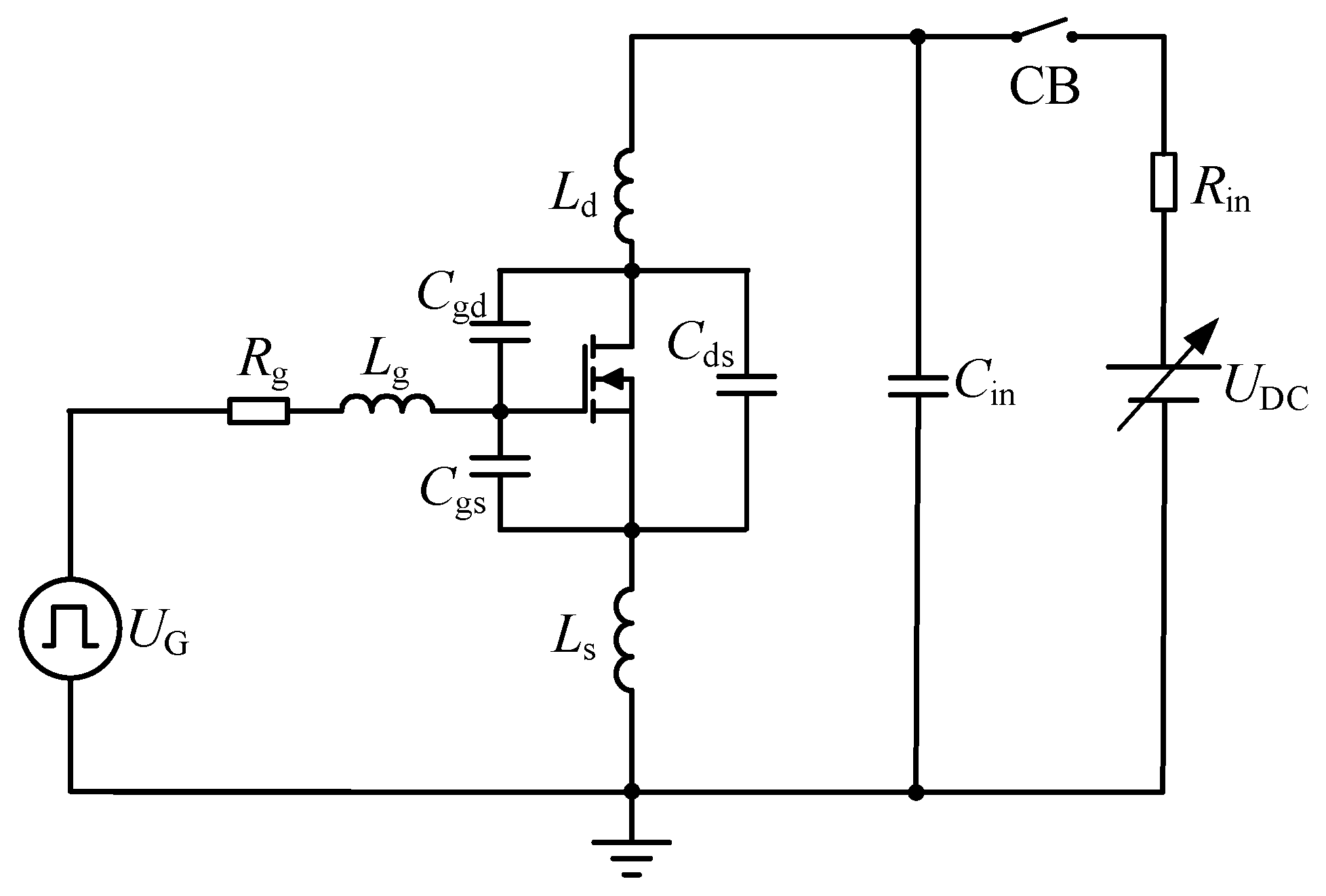
As shown in Figure 4, a pulse test circuit with fast-switching characteristic is presented to measure the short circuit capability of the MOSFET. The input voltage UDC is a controlled DC voltage source, and Rin is the internal resistance of the power source. A single pulse voltage UG is applied to drive the MOSFET with a series connected gate resistor Rg. CB is the circuit breaker. Cgs, Cds, Cgd are parasitic capacitors of the MOSFET. Here, we compare a 1200 V SiC MOSFET (SCH2080KE) and a 1200 V Si MOSFET (IXFH12N120P). Capacitors are noted as Cgs, Cds, Cgd are 1850 pF, 20 pF, 175 pF in SCH2080KE, while Cgs, Cds, Cgd are 5400 pF, 40 pF, 290 pF for IXFH12N120P. This shows that the parasitic capacitors of Si MOSFET are much bigger than those of Si MOSFET. Lg, Ld and Ls are parasitic inductances ranging from 10 nH to 50 nH, and they include all the parasitic inductors of the MOSFET as well as the parasitic inductors of the PCB.
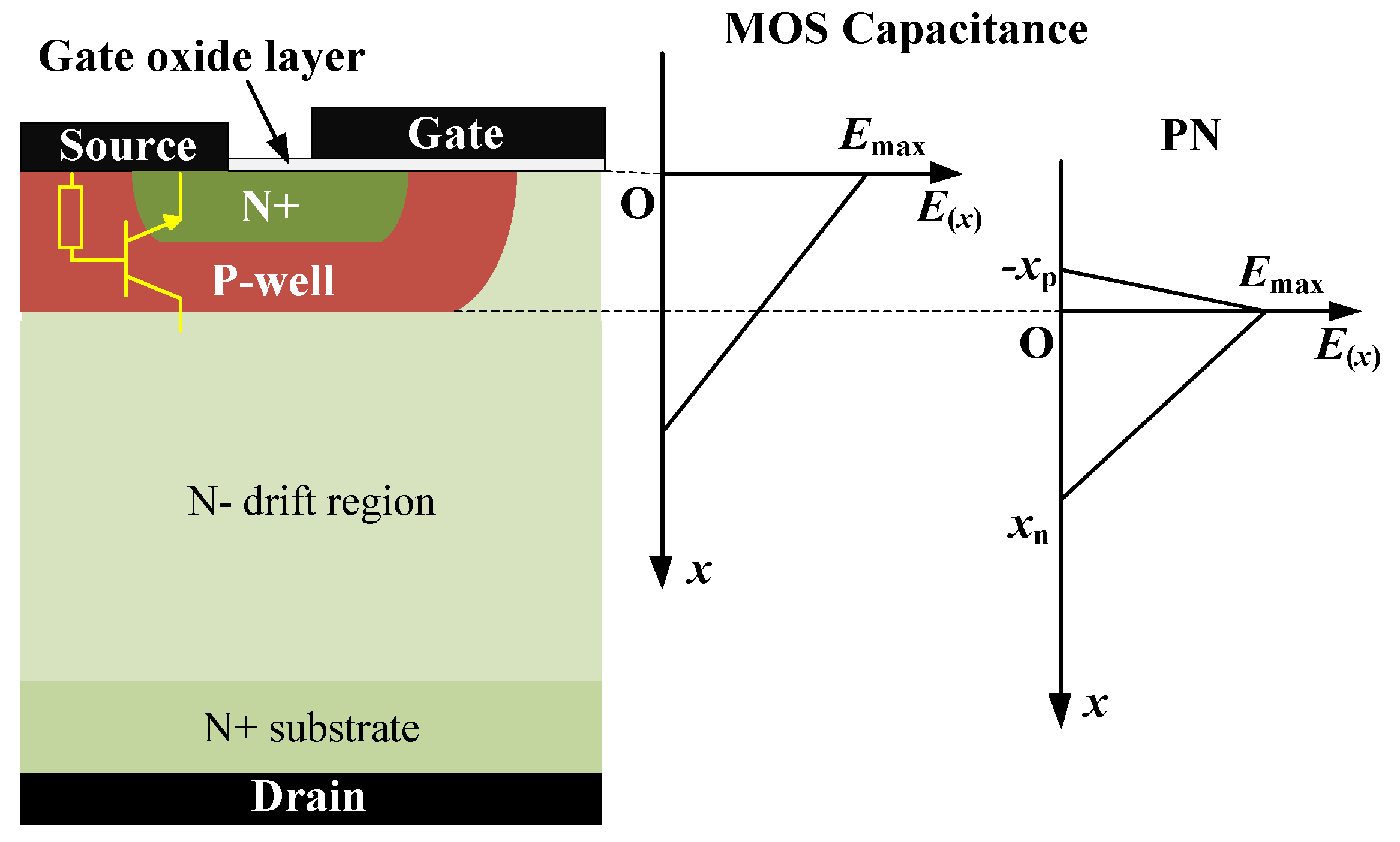
During the short-circuit transient, the DC bus voltage UDC is applied to the MOSFET. Since the gate-source voltage of MOSFET is low, the DC bus voltage is shared by the reverse biased PN junction (the drain-source parasitic capacitor Cds) and MOSFET capacitor (the source-drain parasitic capacitor Cgd). The internal electric field distribution is built as shown in Figure 5.
The electric field developed in the gate oxide is related to the electric field in the underlying semiconductor by Gauss’s Law [28].
E oxide = ε semi ε oxide E max
where Eoxide is the electric field in the semiconductor, εsemi and εoxide are the dielectric constants of the semiconductor and the oxide, respectively, Emax is the maximum value of Eoxide.
The εsemioxide is approximately 2.5 for SiC/SiO2 semiconductor, which means that the electric field strength of the oxide is 2.5 times stronger than that in the semiconductor. The breakdown field strength of SiO2 is 10 MV/cm. According to Equation (6), the electric field strength of the oxide is usually less than 4 MV/cm to ensure long-term stability of the oxide layer. The electric field in the oxide layer with Si material is always at the limit of reliability due to the maximum electric field with 0.3 MV/cm. However, for SiC devices, the maximum electric field is almost 10 times stronger than that of Si devices. Therefore, the oxide will easily reach its reliability limitation and result in the instability of the oxide layer. The intensity of electric field also increases in high voltage applications, which means suitable schemes for the fault detection is needed for SiC MOSFET such as HVDC microgrids. To achieve the desired threshold voltage, the thickness of the gate oxide is designed to be thinner and the barrier is to be narrower. However, the thin layer will cause the reliability issue on the gate, especially when an extremely harsh operation mode is applied. During the short-circuit operation, the excessive temperature rise in the device will also result in the increase of the gate leakage current. This will lead to the breakdown of the oxide dielectric and result in the deterioration of the device when the leakage current reaches a certain value.

4. Short-Circuit Protection

4.1. Current Detection

The short circuit peak current is related to the device package of the MOSFET on the physical structure; from the electrical characteristics, it is also affected by the applied drive voltage, the drain-source voltage, and short-circuit detection method.
Four different kinds of detection method are considered here, and they are resistor detection, transformer detection, Hall current detection, and desaturation detection [29]. Since the considerable power losses are consumed by the resistor when the current flows through it, the resistor detection is not suitable to measure the high current condition. The transformer detection has lower power losses, but it cannot measure the DC current due to the constant magnetic field of the coil [30]. For the Hall current sensor [31], an auxiliary power supply is needed, and it will increase the size and cost of the system. Therefore, with the fast response time and simple configuration, the desaturation detection method is applied in this paper.
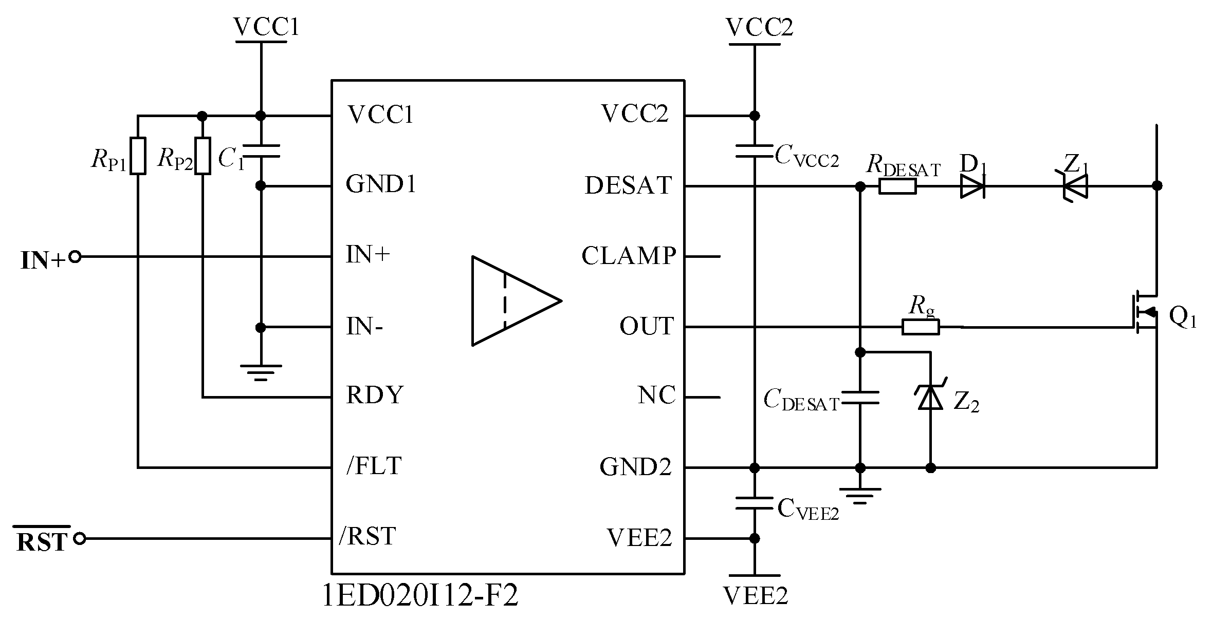
The desaturation detection method is based on the output characteristics of the power device. The drain-source voltage of SiC MOSFET is very low at the conduction state. When the short circuit happens, the drain-source voltage will increase rapidly. The current flowing through the device can be measured by measuring the terminal voltage. Figure 6 shows the peripheral circuit based on the drive IC 1ED020I12-F2 with the function of the desaturation detection [32]. /FLT pin is the fault output, which is used to report the desaturation error of the SiC MOSFET. RDY pin shows the READY status to report the correct operation of the device. DESAT pin is used to monitor the SiC MOSFET voltage (Uds) to detect desaturation caused by the short-circuit current. RP1 and RP2, with the resistance of 10 kΩ, are used to pull up the voltage of RDY and /FLT; C1, CVCC2, CVEE3 are decoupling capacitors of the power supply. The capacitor CDESAT defines the external blanking time of the DESAT pin. Z2 is a protector diode to limit the negative voltage of the input of the DESAT pin. Rg is the external gate resistor of SiC MOSFET. RDESAT, D1 and Z1 are required to limit the current flowing in and out of the DESAT pin.
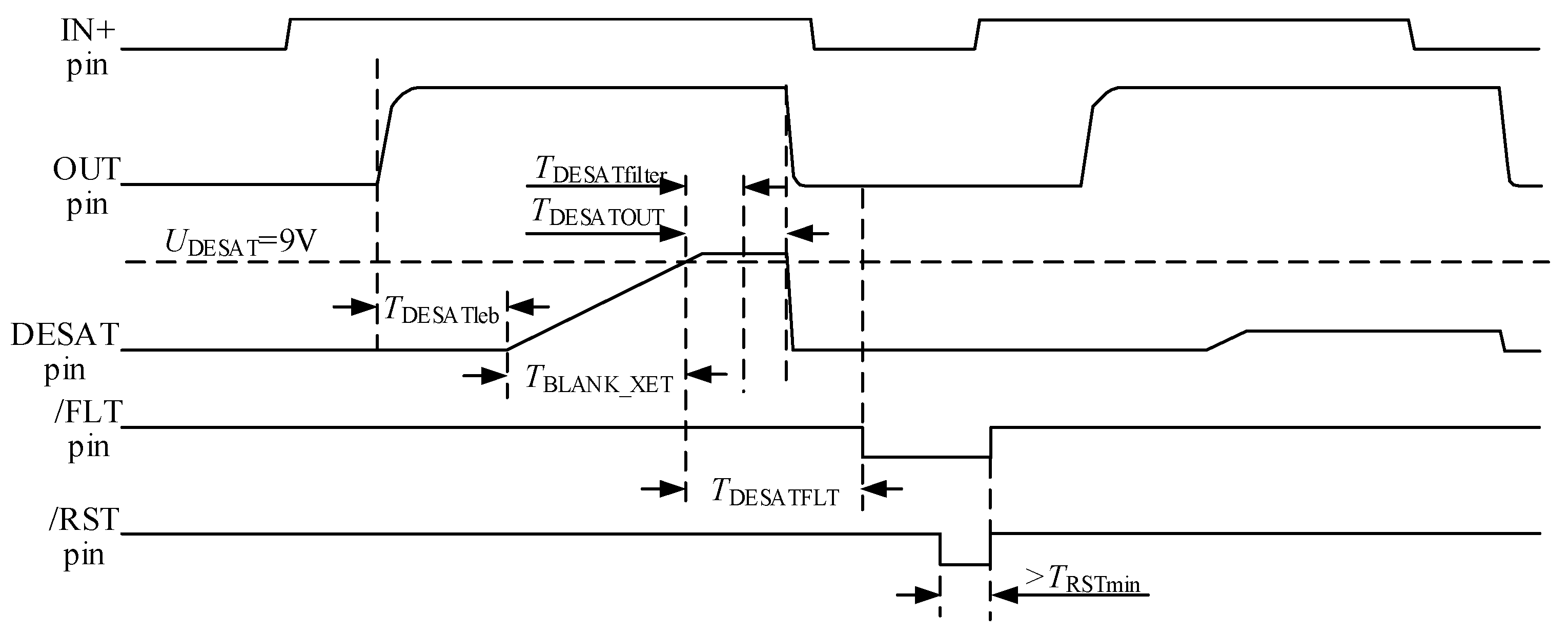
The dynamic behavior of the desaturation detection is shown in Figure 7. When the IN+ pin is high, the OUT pin will jump to high after TPOON delay and the “DESAT” pin is in the state of detection. To ensure safety and to reduce the drain-source voltage of SiC MOSFET during the turn-on transition, a certain blanking time must be considered. The blanking time TBLANK of 1ED020I12-F2 is calculated as:
T BLANK = T DESATleb + T BLANK _ EXT
where, TDESATleb is the frontier blanking time determined by the drive chip with a typical value of 400 ns. The capacitor CDESAT defines the time TBLANK_EXT, and TDESAT_EXT is the external blanking time calculated as:
T BLANK _ EXT = C DESAT × U DESAT I SOURC _ IN
where UDESAT is the trigger voltage for desaturation protection and is set to be 9 V. ISOURCE_IN is the high precision current source of the chip and is set to be 500 µA. In addition, to give a sufficient margin for safety, the blanking time TBLANK must satisfy:
T BLANK > T on
where, Ton is the turn-on time of SiC MOSFET. During the blanking time TBLANK, the UCDESAT can be calculated as:
U CDESAT = U D 1 + U Z 1 + U ds
In which, UD1 is the forward voltage drop of the diode D1, UZ1 is the reverse steady-state voltage of Zener diode Z1, and Uds is the drain-source voltage of the SiC MOSFET. The protection against the different fault currents can be achieved by selecting different Zener diodes Z1.
In the normal state, the drain-source voltage of SiC MOSFET is low and UCDESAT < UDESAT. When FUL happens, UCDESAT will increase with the increase of Uds. When UCDESAT > UDESAT, the protection circuit will work. After the TDESATOUT delay, the OUT pin will output high level, and then SiC MOSFET is turned off. At the same time, UCDESAT decreases gradually to discharge the capacitor CDESAT. After a period of delay, both the /FLT pin and the /RST pin turn to low, indicating a fault condition. The chip is then reset and the output is forced to be zero.
Under HSF condition, Uds approaches to the DC bus voltage, and the diode is reversely cut-off, then UCDESAT will not follow the Equation (10). After the blanking time TBLANK, UCDESAT reaches to UDESAT, the protection circuit will turn off the SiC MOSFET.
After SiC MOSFET turns off, the reverse voltage of D1 is similar to the DC bus voltage, so a high voltage diode should be considered here. Meanwhile, to prevent the voltage noise of the DESAT pin, a 1 kΩ decoupling resistor RDESAT is connected in series to the desaturation detection loop.

4.2. Clamping the Gate-Source Voltage

During the short-circuit condition, the gate-source voltage Ugs will be increased due to the miller current caused by the rapid change of Uds. Then, the short-circuit current will be further increased. Therefore, Ugs must be clamped in the short-circuit condition to inhibit the peak of the short-circuit current [33].
Several passive schemes have been proposed to clamp the gate-source voltage. One method is to put a diode between the gate and source to clamp the gate-source voltage. When the gate voltage reaches a certain clamping value, the diode is turned on and the gate voltage is clamped to the supply voltage. Another method is to connect a Zener diode in a parallel fashion with the gate and source. The circuit design is simple, while the disadvantage is a time delay of the gate voltage detection and a lack of reliability [34].
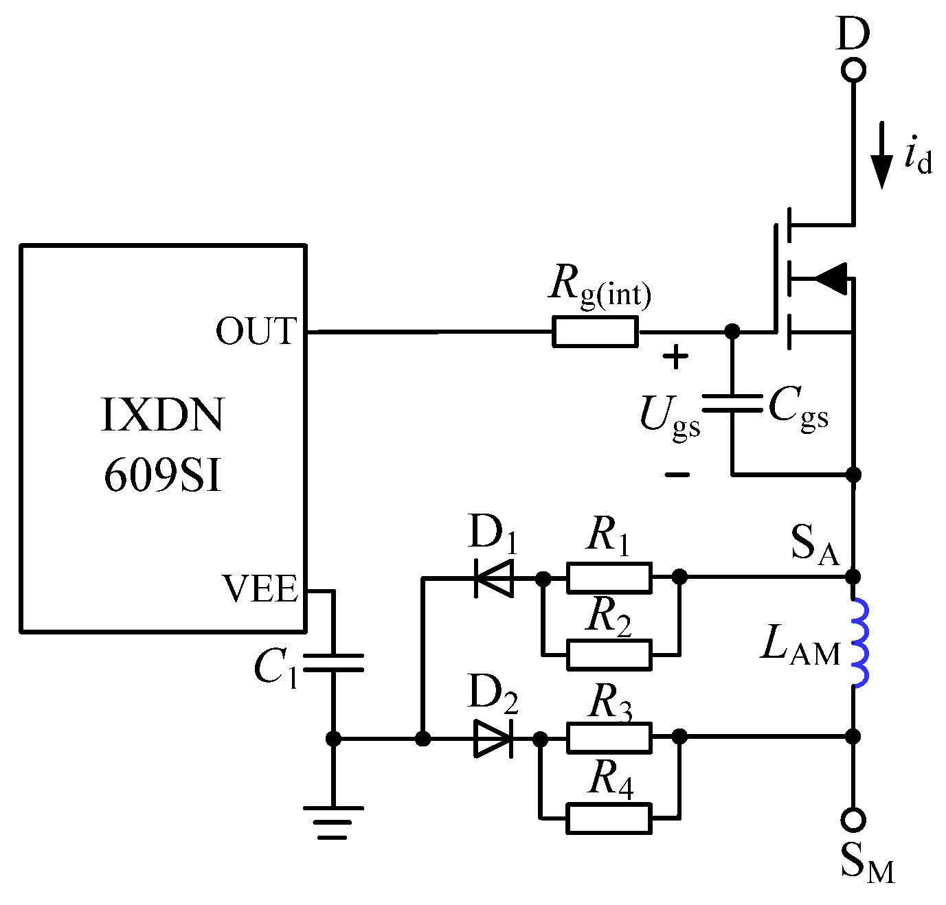
In addition, active schemes can be applied to the SiC MOSFET module with Kelvin structure, where the auxiliary source and main power source are classified. The gate drive circuit is usually connected to the auxiliary source to reduce the parasitic inductors of the gate drive circuit and the oscillation of Ugs. As shown in Figure 8, LAM is the parasitic inductance between the auxiliary source and the main power source of the SiC MOSFET module. The negative feedback of LAM is introduced to reduce the gate-source voltage and restrain the peak of the short circuit current when the short-circuit fault happens. During the turn-off transition of SiC MOSFET, the current flowing through LAM is in a reverse direction. This will induce a reverse voltage against the gate-source voltage Ugs, thus, the turn-off speed will slow down and the voltage overshoot will be inhibited. However, when LAM is too small, the suppression ability will be decreased. Meanwhile, the driver circuit is connected with the auxiliary source, so the high turn-on speed of the SiC MOSFET will not be influenced. This will also shorten the blanking time and speed up the detection speed. In addition, this method can inhibit the voltage overshoot as well.

5. Experiment and Analysis

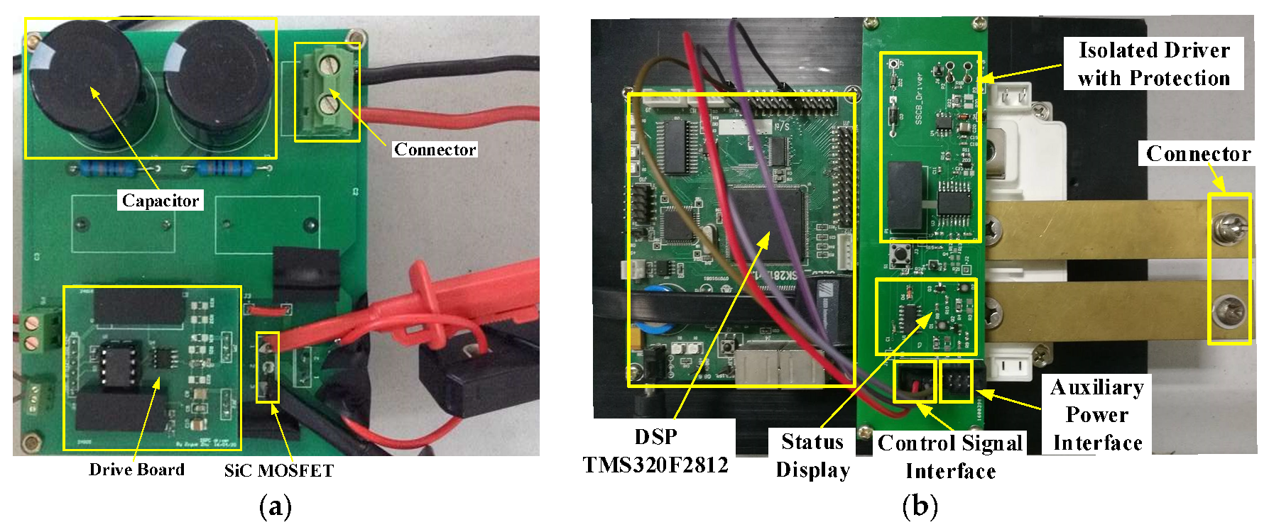
As shown in Figure 9a, a commercially available 1200 V transistor, SCH2080KE from ROHM, was used for the short-circuit test platform, and compared with a 1200 V Si MOSFET IXFH12N120P from IXYS.
To verify the effectiveness of the proposed “soft turn-off” protection method combined with the desaturation detection method, a 270 V/100 A SSCB experimental platform was built, shown in Figure 9b. The PCB layout of the experiment platform was optimized to reduce the inductance of the parasitic inductors.

5.1. Short-Circuit Capability Test

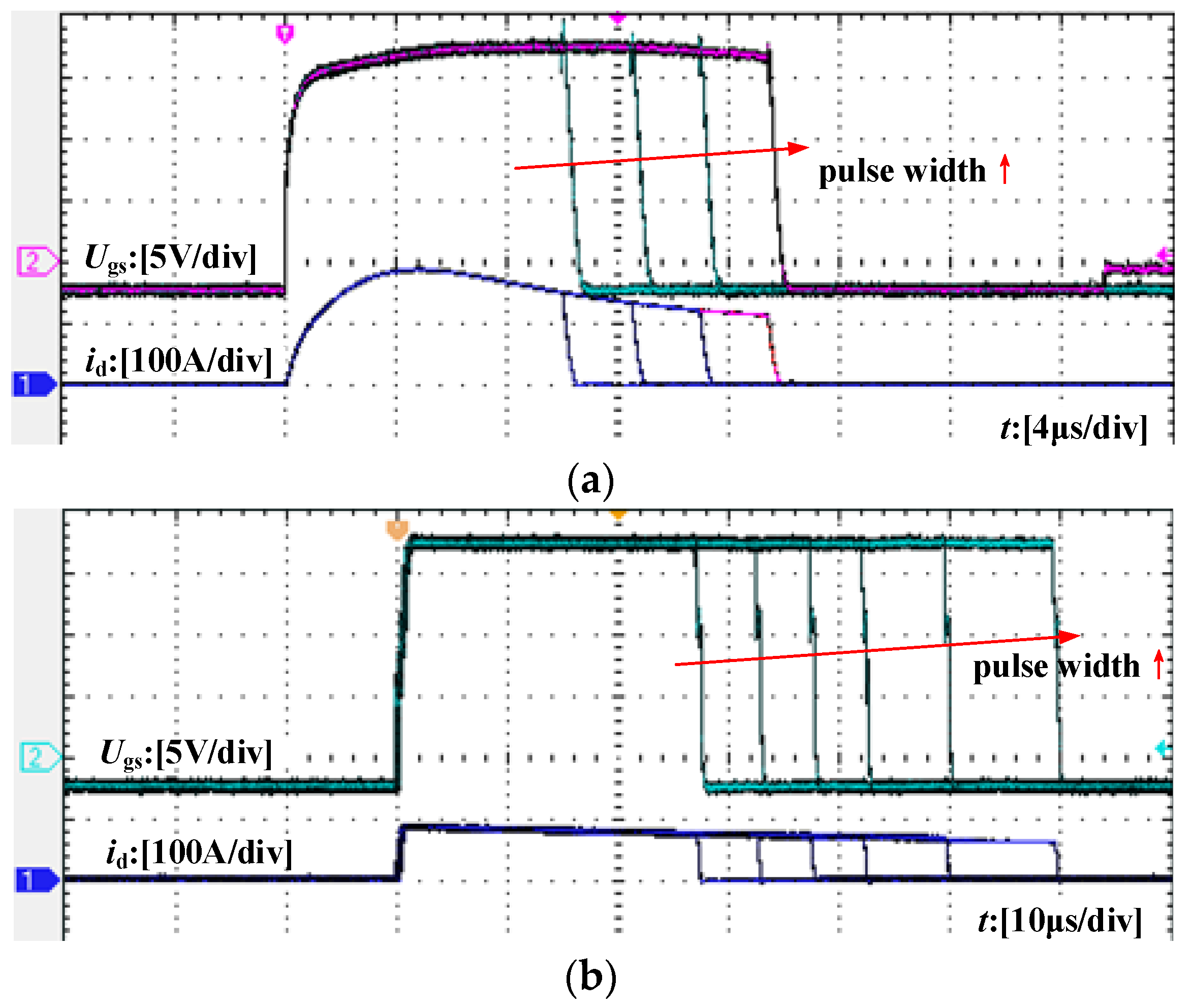
The short-circuit capabilities of Si MOSFET and SiC MOSFET were investigated under different pulse widths, with DC bus voltage of UDC = 550 V and drive resistor Rg = 30 Ω. The positive gate of SiC MOSFET bias was set to be 18 V, as recommended by the device manufacturer.
Figure 10 shows the measured Ugs and id waveforms of SiC MOSFET and Si MOSFET in 550V DC voltage. When the pulse width was 10 μs, the short circuit current increased immediately and then decreased. With the increase of the pulse width, the short circuit current decreased after the SiC MOSFET turned off, but the short-circuit energy kept increasing. When the pulse width increased to 15 μs, the Ugs of SiC MOSFET decreased slightly at the on-state. This indicates that the performance of the device begins to deteriorate with the increase of the gate leakage current. When the pulse width further increased to 17.5 μs, Ugs decreased to 2 V at the on-state. The Ugs will not drop to 0 V until SiC MOSFET has been turned off for 12 μs. This indicated that the gate-source of SiC MOSFET is short-circuited and the device has been destroyed by the high short-circuit energy EC with the value of 1.365 J. However, Si MOSFET maintained good performance when the 17.5 μs pulse width was applied. Even though when the pulse width increased to 60 μs with the short-circuit energy EC of 2.403 J, and showed better short-circuit capability for Si MOSFET.
The parameters of the SiC MOSFET under the normal condition and the damaged condition are shown as Table 1. The date is obtained under the condition with the DC bus voltage of 550 V and the pulse width of 17.5 μs. Under such condition, the gate-source oxide of SiC MOSFET is broken down and the device becomes uncontrolled. However, the drain-source impedance of SiC MOSFET keeps a high value and the device can still block the voltage. Meanwhile, the forward voltage drop of the body diode almost remains unchanged.

5.2. Fault under Load (FUL) Condition Test of SSCB

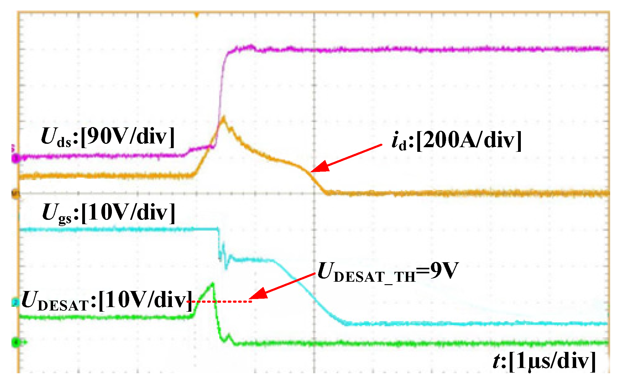
Figure 11 shows the experimental waveforms of drain-source voltage Uds, drain current id, gate-source voltage Ugs and saturation voltage UDESAT of SiC-based SSCB under FUL condition. The load current Id is 100 A. Obviously, the fault response time is only 0.5 µs, benefited from the fault monitor of the DESAT pin on the drain-source voltage of the SiC MOSFET through the diode. When the load falls into a fault, the OUT pin directly reaches a low level after the TDESATOUT delay without the blanking time. Similar to HSF, Ugs rapidly decreases to a certain voltage value, and then slowly reduces to −5 V due to the negative feedback of the parasitic inductor of the source. It can be seen that the full shutdown time of the short-circuit current is about 2.2 µs.

5.3. Hard-Switching Fault (HSF) Condition Test of SSCB

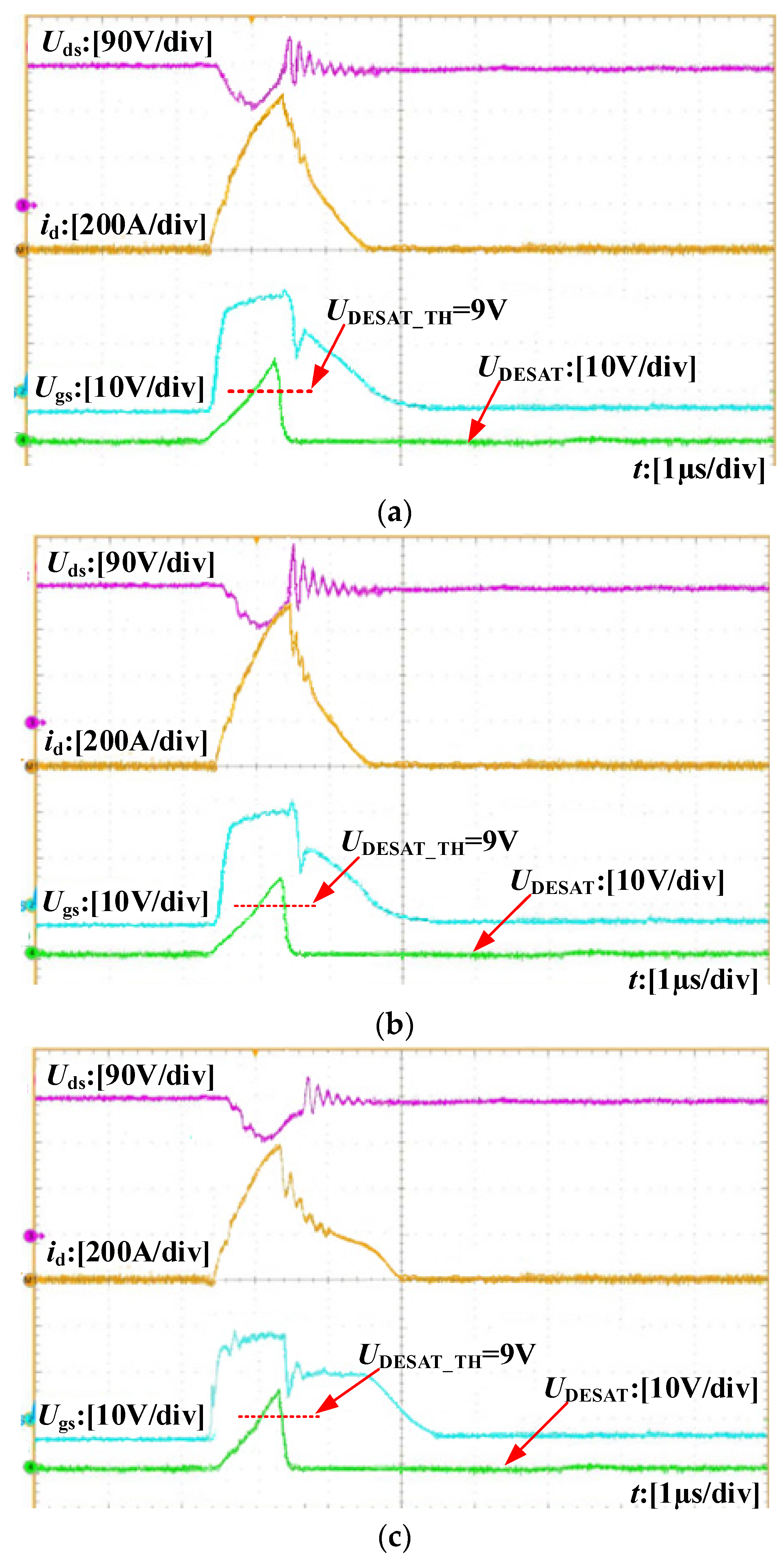
Figure 12 shows the experimental waveforms of the drain-source voltage Uds, the drain current id, the gate-source voltage Ugs and the saturation voltage UDESAT of SiC-based SSCB under the HSF condition. The trigger voltage of UDESAT_TH was 9 V. When the gate-source voltage was clamped, the fault response time of SiC-based SSCB was about 1 µs and the full shutdown time of short-circuit current was about 2 µs. Because of the forward voltage drop of clamping diode, the maximum of gate voltage during the turn-off transition was 20.9 V and the short-circuit peak current is limited to 650 A, and the drain peak voltage is 325 V. With the parallel connection between the gate and source of Zener diode, the fault response time was about 1 µs and the full shutdown time of short-circuit current was about 4 µs. Due to the delay of Zener diode clamping, the maximum gate voltage during the turn-off transition was 21.5 V. Then, the short-circuit peak current increases to 650 A, and the drain peak voltage also increases to 358 V. In contrast, the soft switch-off circuit based on LAM was also tested. The fault response time was about 1 µs and the full shutdown time of short-circuit current was about 4.5 µs. At first, Ugs rapidly decreased to a certain voltage, and then slowly reduced to −5 V due to the negative feedback of the source parasitic inductor. Then, the drain peak voltage was limited to 310 V. When an external Zener diode was connected in series to reduce the trigger voltage for desaturation protection, the peak current of the short-circuit could be further reduced.
The short circuit protection capabilities under different methods are compared in Table 2. The proposed soft turn-off circuit can protect the SiC MOSFET module from being damaged, although the short circuit protection time is slightly extended. The voltage overshoot is reduced, and the short-circuit peak current is also effectively suppressed, which means this method can greatly improve the reliability of the device as well as the SSCB.

6. Conclusions

The paper analyzes the short-circuit characteristics of SiC MOSFET and the change law of the short-circuit current. The device deterioration mechanism of SiC MOSFET is investigated based on the comparison of the short-circuit capabilities between Si MOSFET and SiC MOSFET. To improve the reliability and durability of SiC MOSFET in SSCB under FUL and HSF conditions, a soft switch-off drive circuit based on desaturation detection was developed, and its average response time (2 µs) was less than the range of short-circuit withstanding capacity (4 µs). The experimental results indicated that the proposed protection scheme has the capabilities to reduce the current detection time and the voltage stress of the SiC MOSFET. Also, the short-circuit current was suppressed to improve the switching speed of SiC MOSFET, and the proposed method was suitable for the SSCB based on SiC MOSFET.

Author Contributions

H.Q. and Q.X. conducted the investigation and methodology, Y.M., Y.Z., and Y.D. participated in the experiment and testing, as well as the writing of the original draft.

Funding

This study is funded by the National Natural Science Foundation of China (51677089), Zhejiang Natural Science Foundation under grant No. LY19F030002 and the Fundamental Research Funds for the Central Universities NO.NJ20160047, and NO.NS2015039; and it is under the support by a project funded by the Priority Academic Program Development of Jiangsu Higher Education Institutions. This work is also supported by the Foundation of Graduation Innovation Center at Nanjing University of Aeronautics and Astronautics (kfjj20170308) and the Fundamental Research Funds for the Central Universities.

Acknowledgments

We would like to thank Nanjing University of Aeronautics and Astronautics for the experimental site and measurements. This research is supported by the Center for More Electric Aircraft Power System.

Conflicts of Interest

The authors declare no conflict of interest.

References

  1. Javed, W.; Chen, D.; Farrag, M.E.; Xu, Y. System configuration, fault detection, location, isolation and restoration: A review on LVDC microgrid protections. Energies 2019, 12, 1001. [Google Scholar] [CrossRef]
  2. Nguyen, V.V.; Son, H.I.; Nguyen, T.T.; Kim, H.M.; Kim, C.K. A novel topology of hybrid HVDC circuit breaker for VSC-HVDC application. Energies 2017, 10, 1675. [Google Scholar] [CrossRef]
  3. Hernandez, J.C.; Sutil, F.S.; Vidal, P.G. Protection of a multiterminal DC compact node feeding electric vehicles on electric railway systems, secondary distribution networks, and PV systems. Turk. J. Electr. Eng. Comput. Sci. 2016, 24, 3123–3143. [Google Scholar] [CrossRef]
  4. Hernandez, J.C.; Bueno, P.G.; Sanchez-Sutil, F. Enhanced utility-scale photovoltaic units with frequency support functions and dynamic grid support for transmission systems. IET Renew. Power Gener. 2017, 11, 361–372. [Google Scholar] [CrossRef]
  5. Sanchez-Sutil, F.; Hernández, J.C.; Tobajas, C. Overview of electrical protection requirements for integration of a smart DC node with bidirectional electric vehicle charging stations into existing AC and DC railway grids. Electr. Power Syst. Res. 2015, 122, 104–118. [Google Scholar] [CrossRef]
  6. Pugliese, H.; Von Kannewurff, M. Discovering DC: A primer on DC circuit breakers, their advantages, and design. IEEE Ind. Appl. Mag. 2015, 19, 22–28. [Google Scholar] [CrossRef]
  7. Tan, K.; Liu, P.; Ni, X.; Peng, C.; Song, X.; Huang, A.Q. Performance evaluation of multiple Si and SiC solid state devices for circuit breaker application in 380VDC delivery system. In Proceedings of the 2016 IEEE Applied Power Electronics Conference and Exposition (APEC), Long Beach, CA, USA, 20–24 March 2016; IEEE: Piscataway, NJ, USA, 2016; pp. 983–989. [Google Scholar]
  8. Xun, Q.; Xun, B.; Li, Z. Application of SiC power electronic devices in secondary power source for aircraft. Renew. Sustain. Energy Rev. 2017, 70, 1336–1342. [Google Scholar] [CrossRef]
  9. Nawaz, M.; Ilves, K. Replacing Si to SiC: Opportunities and challenges. In Proceedings of the 2016 46th European Solid-State Device Research Conference (ESSDERC), Lausanne, Switzerland, 12–15 September 2016; IEEE: Piscataway, NJ, USA, 2016; pp. 472–475. [Google Scholar]
  10. Mantooth, H.A.; Peng, K.; Santi, E. Modeling of wide bandgap power semiconductor devices—Part I. IEEE Trans. Electron Devices 2015, 62, 423–433. [Google Scholar] [CrossRef]
  11. Chow, T.P. Wide bandgap semiconductor power devices for energy efficient systems. In Proceedings of the 2015 IEEE 3rd Workshop on Wide Bandgap Power Devices and Applications (WiPDA), Blacksburg, VA, USA, 2–4 November 2015; IEEE: Piscataway, NJ, USA, 2015; pp. 402–405. [Google Scholar]
  12. Sun, J.; Xu, H.; Wu, X.; Yang, S.; Guo, Q.; Sheng, K. Short circuit capability and high temperature channel mobility of SiC MOSFETs. In Proceedings of the 2017 29th International Symposium on Power Semiconductor Devices and IC’s (ISPSD), Sapporo, Japan, 28 May–1 June 2017; IEEE: Piscataway, NJ, USA, 2017; pp. 399–402. [Google Scholar]
  13. Guo, X.; Xun, Q.; Li, Z.; Du, S. Silicon carbide converters and MEMS devices for high-temperature power electronics: A critical review. Micromachines 2019, 10, 406. [Google Scholar] [CrossRef] [PubMed]
  14. Sun, J.; Xu, H.; Wu, X.; Sheng, K. Comparison and analysis of short circuit capability of 1200V single-chip SiC MOSFET and Si IGBT. In Proceedings of the China International Forum on Solid State Lighting: International Forum on Wide Bandgap Semiconductors China, Beijing, China, 15–17 November 2016; IEEE: Piscataway, NJ, USA, 2017; pp. 42–45. [Google Scholar]
  15. Zhang, X.; Sheh, G.; Gant, L.; Banerjee, S. In-Depth Study of Short-Circuit Robustness and Protection of 1200 V SiC MOSFETs. In Proceedings of the PCIM Europe 2018 International Exhibition and Conference for Power Electronics, Intelligent Motion, Renewable Energy and Energy Management, Nuremberg, Germany, 5–7 June 2018; VDE: Berlin, Germany, 2018; pp. 1–7. [Google Scholar]
  16. Urciuoli, D.P.; Veliadis, V.; Ha, H.C.; Lubomirsky, V. Demonstration of a 600-V, 60-A, bidirectional silicon carbide solid-state circuit breaker. In Proceedings of the 2011 Twenty-Sixth Annual IEEE Applied Power Electronics Conference and Exposition (APEC), Fort Worth, TX, USA, 6–11 March 2011; IEEE: Piscataway, NJ, USA, 2011; pp. 354–358. [Google Scholar] [Green Version]
  17. Miao, Z.; Sabui, G.; Chen, A.; Li, Y.; Shen, Z.J.; Wang, J.; Shuai, Z.; Luo, A.; Yin, X.; Jiang, M. A self-powered ultra-fast DC solid state circuit breaker using a normally-on SiC JFET. In Proceedings of the 2015 IEEE Applied Power Electronics Conference and Exposition (APEC), Charlotte, NC, USA, 15–19 March 2015; IEEE: Piscataway, NJ, USA, 2015; pp. 767–773. [Google Scholar]
  18. Sato, Y.; Tanaka, Y.; Fukui, A.; Yamasaki, M.; Ohashi, H. SiC-SIT Circuit Breakers with Controllable Interruption Voltage for 400-V DC Distribution Systems. IEEE Trans. Power Electron. 2014, 29, 2597–2605. [Google Scholar] [CrossRef]
  19. Ren, Y.; Yang, X.; Zhang, F.; Wang, F.; Tolbert, L.M.; Pei, Y. A Single Gate Driver Based Solid-State Circuit Breaker Using Series Connected SiC MOSFETs. IEEE Trans. Power Electron. 2019, 34, 2002–2006. [Google Scholar] [CrossRef]
  20. Marroqui, D.; Blanes, J.M.; Garrigós, A.; Gutiérrez, R. Gutiérrez. Self-Powered 380V DC SiC Solid-State Circuit Breaker and Fault Current Limiter. IEEE Trans. Power Electron. 2019, 34, 9600–9608. [Google Scholar] [CrossRef]
  21. Pilvelait, B.; Gold, C.; Marcel, M. A High Power Solid State Circuit Breaker for Military Hybrid Electric Vehicle Applications. In Proceedings of the 2012 Ground Vehicle Systems Engineering and Technology Symposium (GVSETS), Arlington, VA, USA, 14–16 August 2012. [Google Scholar]
  22. Zhou, Y.; Feng, Y.; Liu, T.; Shen, Z.J. A Digital-Controlled SiC-Based Solid State Circuit Breaker with Soft-Start Function for DC Microgrids. In Proceedings of the 2018 9th IEEE International Symposium on Power Electronics for Distributed Generation Systems (PEDG), Charlotte, NC, USA, 25–28 June 2018; IEEE: Piscataway, NJ, USA, 2018; pp. 1–7. [Google Scholar]
  23. Zhang, L.; Woodley, R.; Song, X.; Sen, S.; Zhao, X.; Huang, A.Q. High current medium voltage solid state circuit breaker using paralleled 15kV SiC ETO. In Proceedings of the 2018 IEEE Applied Power Electronics Conference and Exposition (APEC), San Antonio, TX, USA, 4–8 March 2018; IEEE: Piscataway, NJ, USA, 2018; pp. 1706–1709. [Google Scholar]
  24. Gu, C.; Wheeler, P.; Castellazzi, A.; Watson, A.J.; Effah, F. Semiconductor Devices in Solid-State/Hybrid Circuit Breakers: Current Status and Future Trends. Energies 2017, 10, 495. [Google Scholar] [CrossRef]
  25. Li, H.; Yu, R.; Zhong, Y.; Yao, R.; Liao, X.; Chen, X. Design of 400 V Miniature DC Solid State Circuit Breaker with SiC MOSFET. Micromachines 2019, 10, 314. [Google Scholar] [CrossRef] [PubMed]
  26. Pérez-Tomás, A.; Brosselard, P.; Godignon, P.; Millán, J.; Mestres, N.; Jennings, M.R.; Mawby, P.A. Field-effect mobility temperature modeling of 4H-SiC metal-oxide-semiconductor transistors. J. Appl. Phys. 2006, 100, 114508. [Google Scholar] [CrossRef]
  27. Wang, Z.; Shi, X.; Tolbert, L.M.; Wang, F.; Blalock, B.J. Temperature-dependent short-circuit capability of silicon carbide power mosfets. IEEE Trans. Power Electron. 2015, 31, 1555–1566. [Google Scholar] [CrossRef]
  28. Nguyen, T.T.; Ahmed, A.; Thang, T.V.; Park, J.H. Gate Oxide Reliability Issues of SiC MOSFETs Under Short-Circuit Operation. IEEE Trans. Power Electron. 2015, 30, 2445–2455. [Google Scholar] [CrossRef]
  29. Bertelshofer, T.; März, A.; Bakran, M.M. A temperature compensated overcurrent and short-circuit detection method for SiC MOSFET modules. In Proceedings of the 2017 19th European Conference on Power Electronics and Applications (EPE’17 ECCE Europe), Warsaw, Poland, 11–14 September 2017; IEEE: Piscataway, NJ, USA, 2017; pp. 1–10. [Google Scholar]
  30. Mocevic, S. Phase Current Sensor and Short-Circuit Detection based on Rogowski Coils Integrated on Gate Driver for 1.2 kV SiC MOSFET Half-Bridge Module. In Proceedings of the 2018 IEEE Energy Conversion Congress and Exposition (ECCE), Portland, OR, USA, 23–27 September 2018; IEEE: Piscataway, NJ, USA, 2018; pp. 393–400. [Google Scholar]
  31. Maerz, A.; Bertelshofer, T.; Horff, R.; Bakran, M.M. Requirements of short-circuit detection methods and turn-off for wide band gap semiconductors. In Proceedings of the CIPS 2016 9th International Conference on Integrated Power Electronics Systems, Nuremberg, Germany, 8–10 March 2016; VDE: Berlin, Germany, 2016; pp. 1–6. [Google Scholar]
  32. Infineon Technologies, No. 1ED020I12-F2 Datasheet. Available online: https://www.infineon.com/dgdl/Infineon-1ED020I12-F2-DS-v02_01-EN.pdf?fileId=db3a304330f68606013122ce5f3649cb (accessed on 22 July 2019).
  33. Awwad, A.E.; Dieckerhoff, S. Short-circuit evaluation and overcurrent protection for SiC power MOSFETs. In Proceedings of the 2015 17th European Conference on Power Electronics and Applications (EPE’15 ECCE-Europe), Geneva, Switzerland, 8–10 September 2015; IEEE: Piscataway, NJ, USA, 2015; pp. 1–9. [Google Scholar]
  34. Kreutzer, O.; Eckardt, B.; Maerz, M. Optimum gate driver design to reach SiC-MOSFET’s full potential—Speeding up to 200 kV/μs. In Proceedings of the 2015 IEEE 3rd Workshop on Wide Bandgap Power Devices and Applications (WiPDA), Blacksburg, VA, USA, 2–4 November 2015; IEEE: Piscataway, NJ, USA, 2015; pp. 41–46. [Google Scholar]
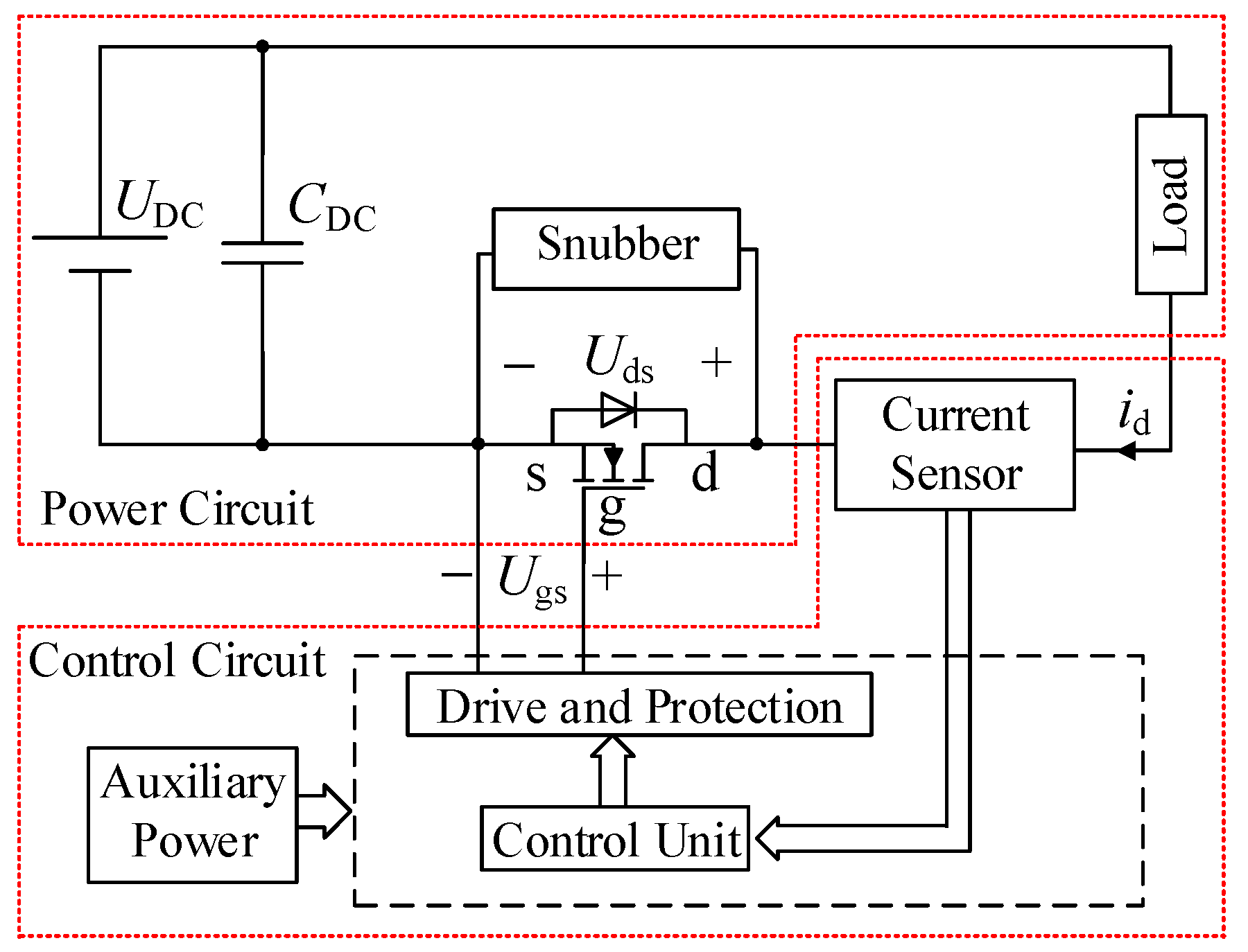
Figure 1. The schematic diagram of solid state circuit breaker(SSCB).
Electronics 08 00837 g001
Figure 2. Operating principles of SSCB.
Electronics 08 00837 g002
Figure 3. Short-circuit waveforms of SiC MOSFET for hard-switching fault.
Electronics 08 00837 g003
Figure 4. Schematic of the test circuit.
Electronics 08 00837 g004
Figure 5. The internal electric field of SiC MOSFET.
Electronics 08 00837 g005
Figure 6. The desaturation detection peripheral circuit based on 1ED020I12-F2.
Electronics 08 00837 g006
Figure 7. The time sequence of the desaturation detection.
Electronics 08 00837 g007
Figure 8. Soft switching-off circuit.
Electronics 08 00837 g008
Figure 9. The experiment platform: (a) short-circuit TEST platform of MOSFET; (b) short-circuit TEST platform of SSCB.
Electronics 08 00837 g009
Figure 10. Short-circuit waveforms of Ugs, and id under different pulse width: (a) wave of SiC MOSFET; (b) wave of Si MOSFET.
Electronics 08 00837 g010
Figure 11. Experiment waveform of Uds, id, Ugs, UDESAT under FUL.
Electronics 08 00837 g011
Figure 12. Short-circuit waveforms under different clamping methods: (a) gate-source voltage clamping; (b) Zener diode clamping; (c) soft switching-off circuit.
Electronics 08 00837 g012
Table 1. The terminal impedance and body diode forward voltage drop SiC MOSFET.
ParametersSiC MOSFET (SCH2080KE)
NormalDamaged
Rgs/Rsg (Ω)∞/∞0.8/0.8
Rgd/Rdg (Ω)∞/∞∞/∞
Rds/Rsd (Ω)∞/∞∞/∞
UF (V)0.6770.680
Table 2. Test data of short circuit protection under different methods.
Gate-source Voltage VlampingZener Diode ClampingSoft Turn-Off Circuit
Short-circuit peak current (A)650700600
Overshoot voltage (V)325358310
Short-circuit protection time (µs)222.5