Article

A Charge-Sharing-Based Two-Phase Charging Scheme for Zero-Crossing-Based Integrator Circuits

School of Electronics Engineering, Kyungpook National University, Daegu 41566, Korea
*
Author to whom correspondence should be addressed.
Electronics 2019, 8(7), 821; https://doi.org/10.3390/electronics8070821
Submission received: 27 June 2019 / Revised: 19 July 2019 / Accepted: 22 July 2019 / Published: 23 July 2019
(This article belongs to the Section Circuit and Signal Processing)

Abstract

:
As an effort to improve the energy efficiency of switched-capacitor circuits, zero-crossing- based integrators (ZCBI) that consist of zero-crossing detectors and charging circuits have been proposed. To break the trade-off between accuracy and speed, ZCBI typically employs a two-phase charging scheme that relies on an additional threshold for zero-crossing detection. This paper proposes a simpler realization method of the two-phase charging scheme by means of charge sharing. To demonstrate feasibility of the proposed method, we designed and fabricated a second-order delta-sigma modulator in 180-nm complementary metal–oxide–semiconductor (CMOS) technology. The measurement results show that the modulator exhibits a peak signal-to-noise-and-distortion ratio (SNDR) of 46.3 dB over the bandwidth of 156 kHz with the power consumption of 684 µW. We also designed the same modulator in 65-nm CMOS technology and simulation results imply that the proposed circuit is able to achieve a much better energy efficiency in advanced technology.

1. Introduction

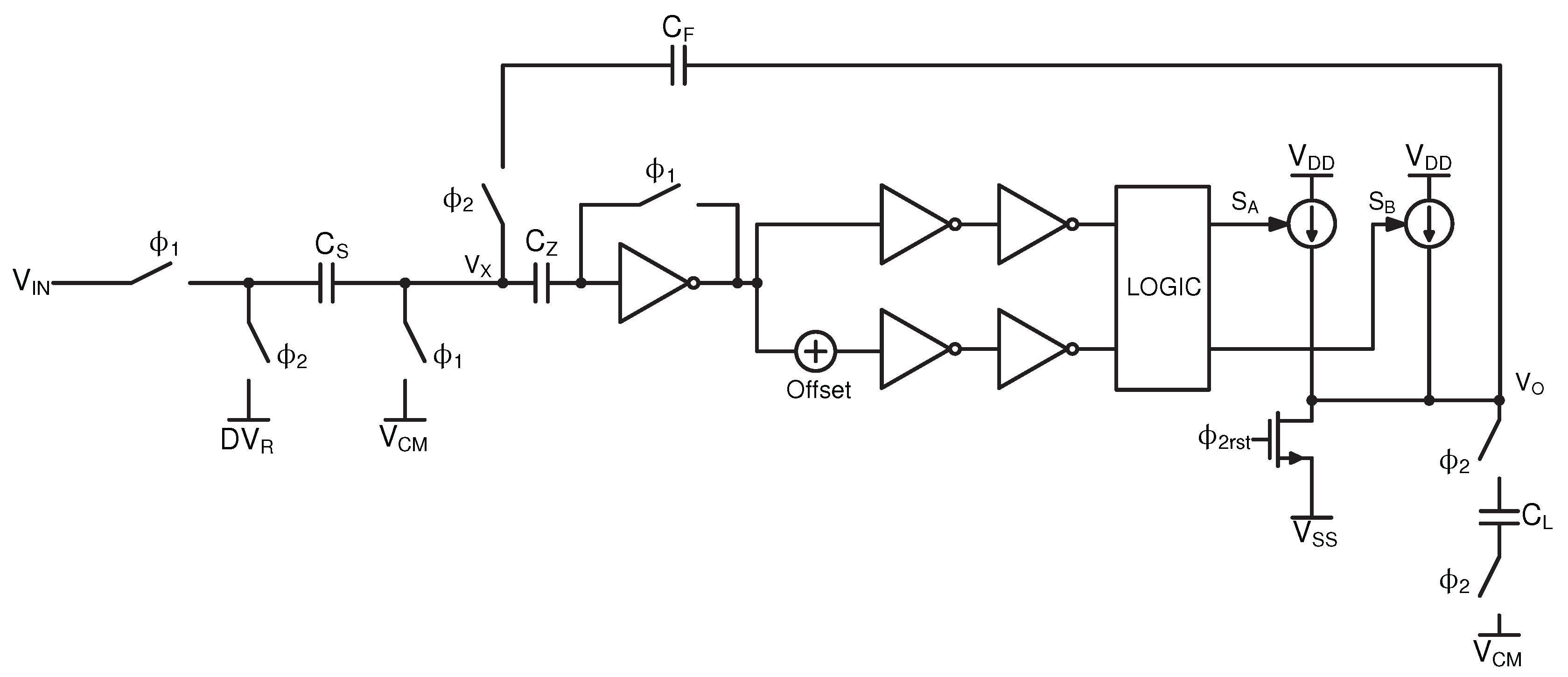
In conventional switched-capacitor integrators, the negative feedback around an operational transconductance amplifer (OTA) with a high DC gain forces the two input terminals to have the same potential, controlling the charge transfer from the sampling capacitor to the feedback capacitor. In advanced technology with a reduced supply voltage, however, achieving the high DC gain is not straightforward. In addition, conventional OTAs are not power efficient due to their typical class-A operation [1,2,3,4]. As an alternative, zero-crossing-based integrator (ZCBI) circuits have been proposed (Figure 1a) [5,6,7,8,9,10,11,12,13,14,15,16], where zero-crossing-detectors (ZCD) and current sources are used to control the charge transfer.
As the timing diagram in Figure 1b shows, the finite delay of the ZCD causes an overshoot at the input of ZCD and consequently at the integrator output. If the current source charges the load with the constant current I, the overshoot voltage at the output of the integrator is given by
V OVS = I × t d C LD ,
where t d is the delay of the ZCD and C LD is the total capacitance at the output of the integrator [11]. The overshoot voltage manifests itself as a DC offset at the integrator output, which is not detrimental. However, if the charging current is governed by a resistor R S , whether it be the output resistance of a transistor current source or a kind of current source itself, the overshoot voltage has the additional gain error component as expressed in
V OVS = ( V DD V O ) ( 1 e t d τ ) ,
where τ = R S C LD is the time constant. The gain error term modifies the gain and the pole location of the integrator transfer function. More importantly, the current value at the zero-crossing moment and thus the delay t d become signal-dependent causing nonlinearity in the overshoot voltage [11]. The nonlinearity due to signal-dependent t d can be reduced by increasing the time constant, but it comes at the cost of reduced speed of the integrator. The trade-off relationship between speed and accuracy can be alleviated by two-phase charging schemes [5,6,10,11,12,13,14]. In a two-phase charging scheme, the charge transfer phase is divided into two phases: coarse and fine. During the coarse phase, a high current is used to make V X approach V CM quickly; then, during the fine phase, a low current is used to reduce the overshoot. Depending on the direction of charging during the fine phase, the two-phase charging scheme can be bidirectional or unidirectional (Figure 2). If the charging scheme is bidirectional, the coarse phase ends when the ZCD detects zero-crossing through the threshold V CM . During the fine phase, the overshoot voltage is compensated for by the low current of the opposite direction. The unidirectional two-phase charging scheme, on the other hand, introduces an additional threshold V th that is lower than V CM to decide when to make a transition from the coarse phase to the fine phase. The bidirectional scheme is simpler in a sense that it needs only one ZCD. However, it requires greater headroom to accommodate the large overshoot at the end of the coarse phase. With a low supply voltage, therefore, the unidirectional scheme is preferred over the bidirectional scheme.
In [15], we have shown that charge sharing can be used to implement the unidirectional two-phase charging scheme without an explicit additional ZCD. This paper presents, in more detail, the design of a second-order Δ Σ analog-to-digital convertor (ADC) that employs the proposed two-phase charging scheme and discusses its effectiveness with measurement results. This paper is organized as follows. Section 2 describes the ZCBI structure that employs the proposed two-phase charging scheme. Section 3 presents the circuit implementation of the fabricated second-order Δ Σ modulator and its measurement results. Effectiveness of the proposed scheme is also discussed. In Section 4, conclusions are drawn.

2. Proposed ZCBI Circuit

Unlike the clocked comparator in most ADCs, the ZCD in Figure 1 needs to continuously monitor whether V X crosses the threshold V CM or not. Therefore, there is a possibility that the ZCD consumes a great deal of static power. In order to reduce the static power consumption of ZCD, an inverter-based ZCD can be used in lieu of conventional comparator circuits as illustrated in Figure 3[16]. The ZCD consists of an inverter and an auto-zeroing capacitor ( C Z ). During the sampling phase ( ϕ 1 is on), the auto-zeroing capacitor samples the voltage difference between V CM and the threshold voltage of the inverter. As a result, the inverter output flips when V X crosses V CM in the charge transfer phase ( ϕ 2 is high). Unfortunately, the inverter output may not be large enough to immediately turn off the current source resulting in a long ZCD delay, especially when the charging current is small. To address this issue, an additional inverter chain is added at the output of the ZCD. However, the inverter chain may increase the effective time delay of the ZCD and it is therefore imperative to make sure that the inverter chain is fast enough to keep the delay as small as possible.
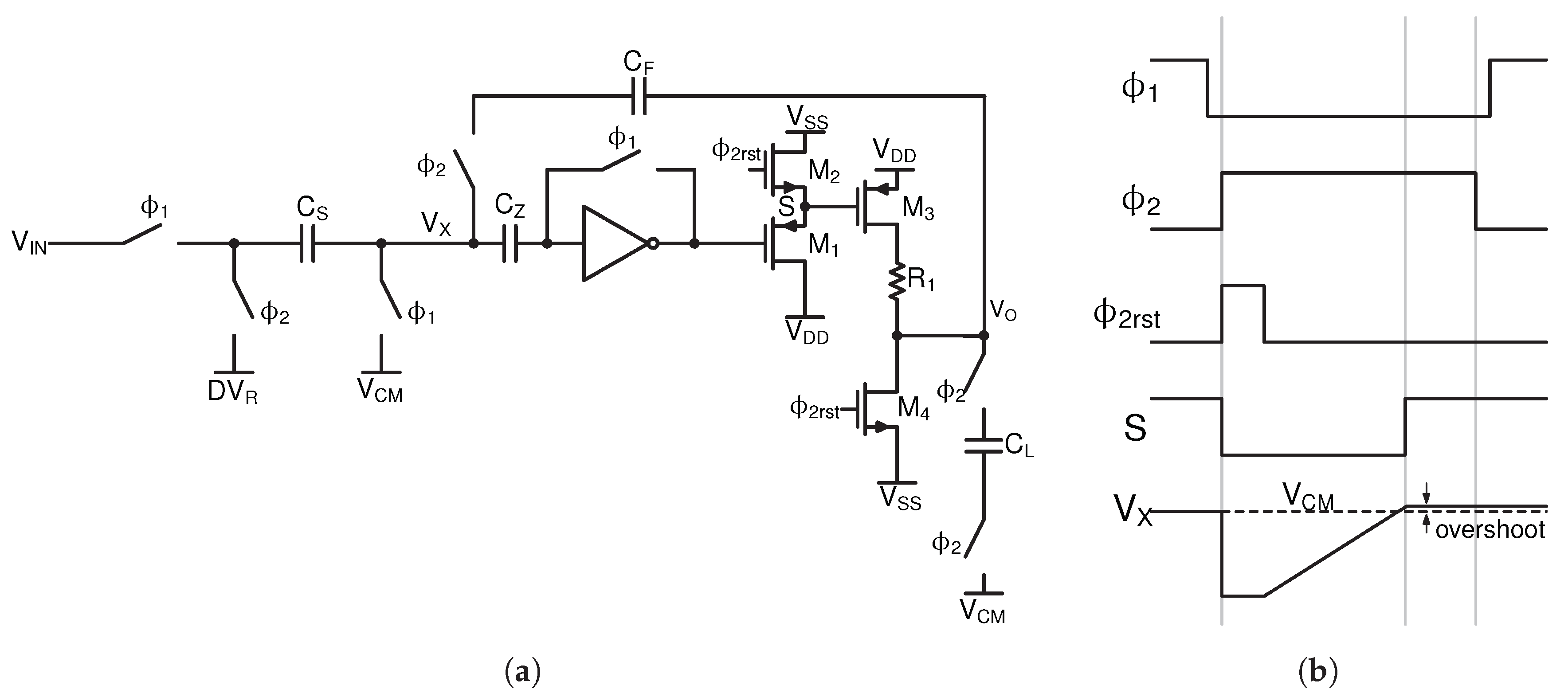
Figure 4 shows our implementation of the inverter-based ZCD, where the inverter is followed by a dynamic buffer. When ϕ 2 rst goes high for a short period of time at the beginning of the charge transfer phase, M 2 is turned on and the gate terminal of M 3 is pre-charged to V SS thus turning on M 3 . The output node is also reset to V SS making V X lower than V CM in all circumstances. As a result, the inverter output becomes high turning off M 1 . When V X crosses V CM , M 1 is turned on and it can quickly charge the gate of M 3 to turn it off since M 2 is already in the off state.
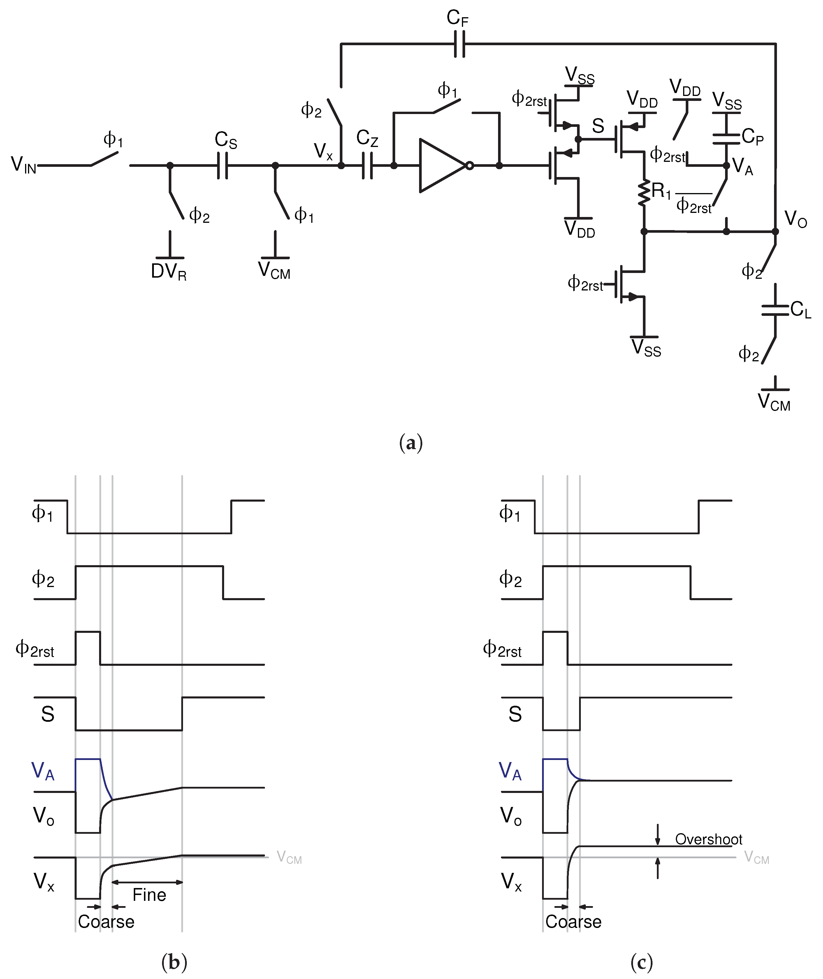
Although the ZCD delay can be reduced to some degree by the use of a dynamic buffer, a two-phase charging scheme still needs to be implemented to break the speed-accuracy trade-off. Figure 5 illustrates the proposed ZCBI circuit that implements a simple unidirectional two-phase charging scheme. The basic idea behind the proposed scheme is to supply a fixed amount of charge during the coarse phase by using a capacitor rather than a current source. It is equivalent to charging by a current source for a fixed duration of the coarse phase. However, the proposed method does not require either an additional ZCD with a different threshold or an additional control signal to make a transition from the coarse to the fine phase. In Figure 5a, C P is pre-charged to V DD during the reset phase. When the charge transfer phase starts, C P is connected to the output node and the charges stored on C P are shared with other capacitors that are connected to the output node, thus the output voltage being raised instantaneously. After charge sharing, the circuit operates the same way as a conventional two-phase charging scheme in the fine phase. In effect, the charge sharing serves as the coarse phase in a conventional two-phase charging scheme.
For proper operation of the proposed two-phase charging scheme, however, the amount of charge to be shared must be well controlled. If V X is greater than V CM at the end of charge sharing, there is no way to discharge the capacitors, ending up with overshoot (Figure 5c). Therefore, the capacitance of C P should be carefully chosen so that V X is lower than V CM under all circumstances when charge sharing is completed. The voltage at the end of charge sharing is expressed as
V X = V X | reset + C P C F C P C F + C L C F + C S C F + C S C P + C S C L V DD ,
where V X | reset is the value of V X at the end of reset phase and is given by
V X | reset = C S C S + C F D V R C S C S + C F v i [ n ] C F C S + C F v o [ n 1 ] .
In Equation (4), D V R is the value of the feedback DAC; v i and v o are small-signal input and output voltages of the integrator, respectively. Substituting the full-scale value for D V R , v i , and v o gives us the upper bound of V X | reset , but it is only a loose bound and places more constraint on the size of C p than required. Alternatively, a more practical value of C p can be found using the distribution of V X | reset , which can be obtained as outlined in the next section.

3. Circuit Implementation and Measurement Results

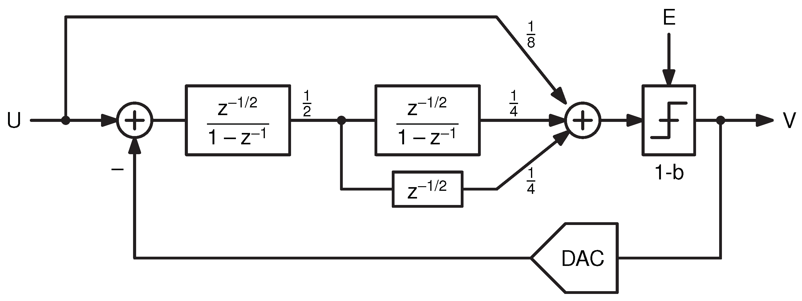
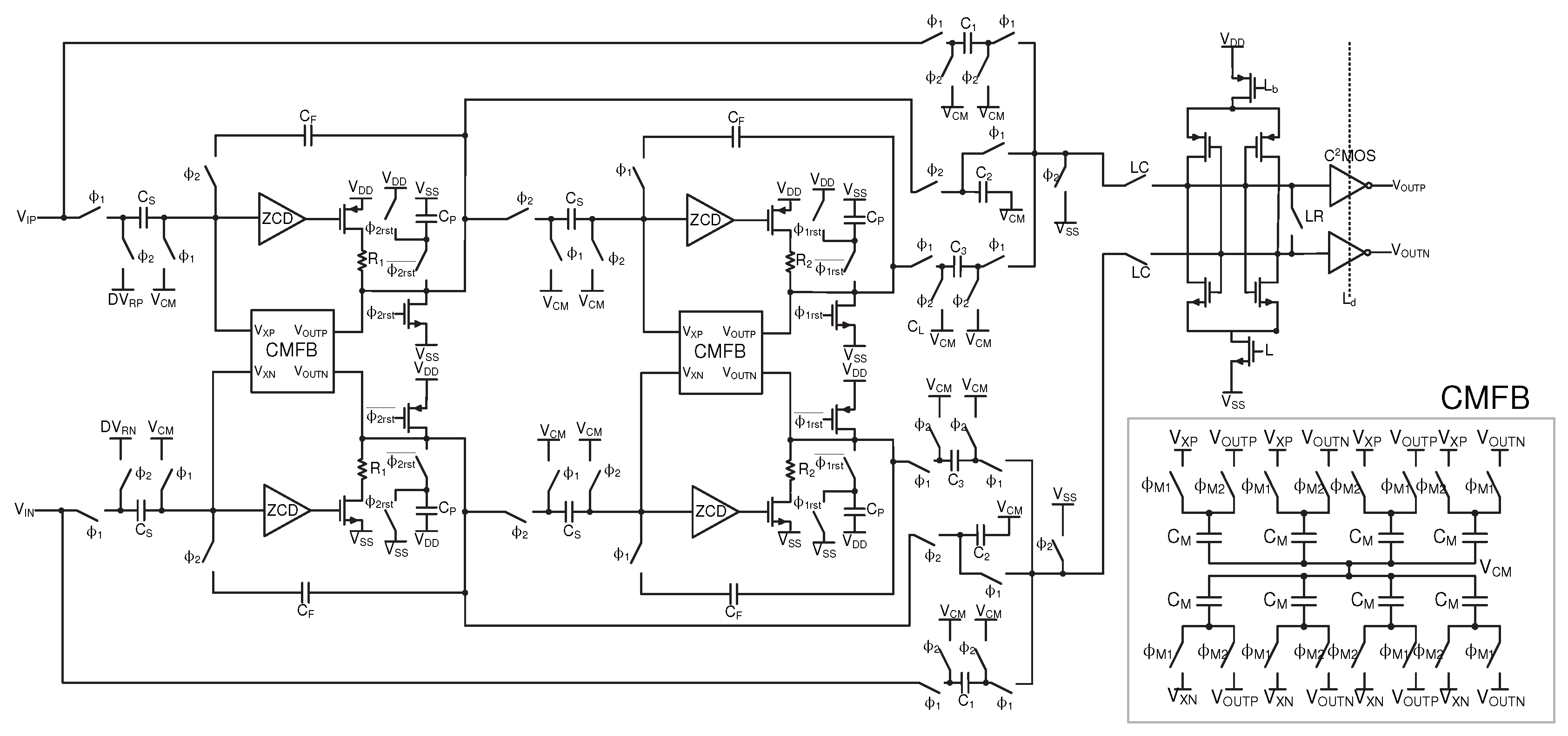
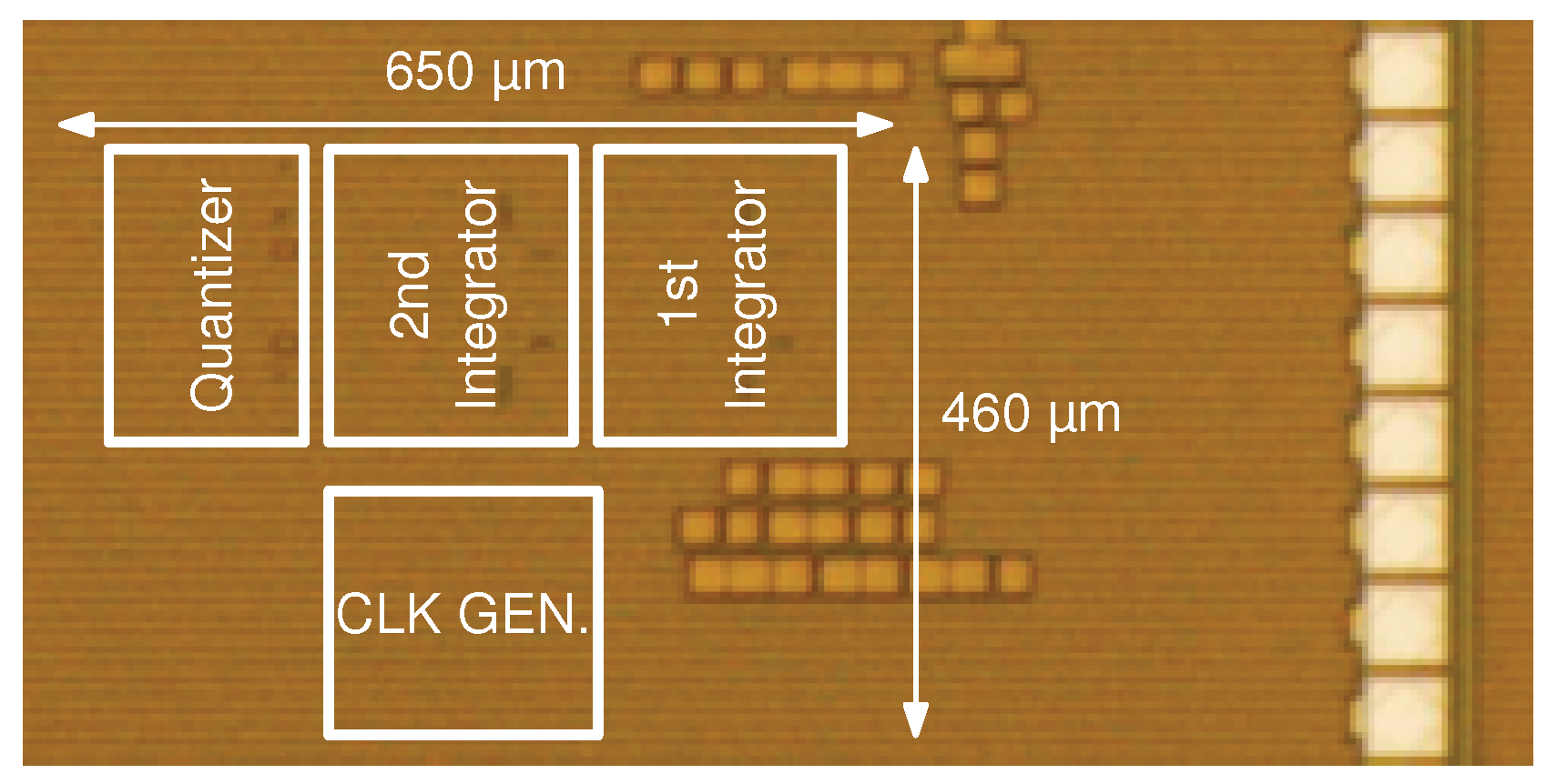
In order to demonstrate feasibility of the proposed technique, a second-order Δ Σ modulator has been fabricated in 180-nm complementary metal–oxide–semiconductor (CMOS) technology. As shown in Figure 6, the modulator is a low-distortion feedforward structure [17] with a 1-bit quantizer. Figure 7 shows the schematic diagram of the modulator. The half-delay integrators are realized with the proposed ZCBI circuits in pseudo differential form, which include switched-capacitor common-mode feedback circuits [18]. The integrator outputs are combined with the modulator input by the adder in front of the 1-bit quantizer. The adder is realized as a switched-capacitor passive adder for low power consumption. The 1-bit quantizer consists of a dynamic latch, which is basically cross-coupled inverters, and C 2 MOS buffers [19]. The internal clock generator (not shown in Figure 7) creates various non-overlapping clock signals. The nominal clock frequency is 10 MHz and the intended oversampling ratio (OSR) is 32. Figure 8 shows the chip micrograph. The modulator core occupies 0.3 mm 2 . Table 1 shows the summary of the modulator design.
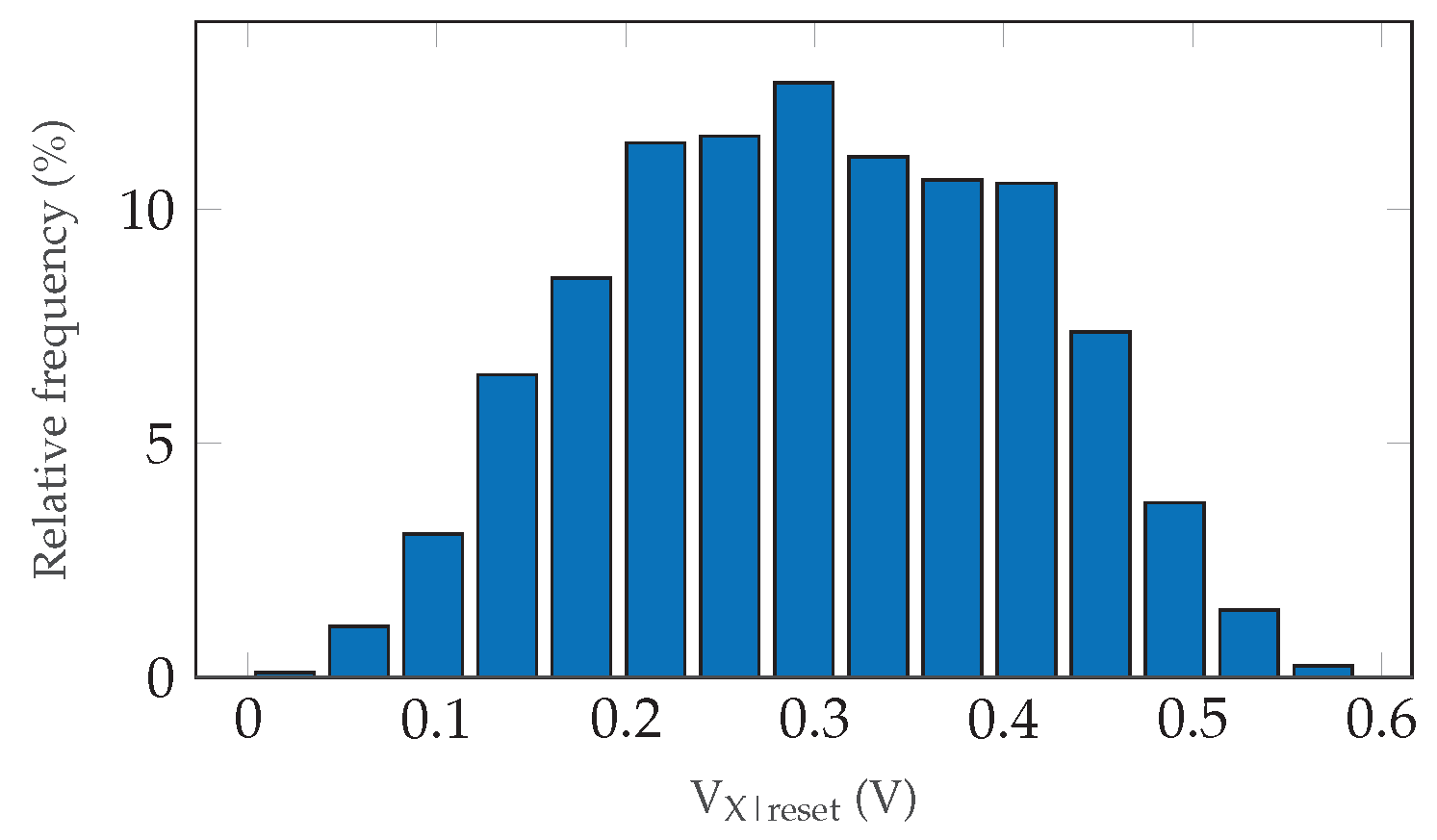
As described in Section 2, the capacitance for charge sharing should be judiciously chosen for proper operation of the ZCBIs. The modulator in Figure 6 and Figure 7 was simulated with behavioral and transistor-level models for various amplitudes and frequencies of single-tone and multi-tone inputs. Figure 9 shows one instance of the distribution of V X | reset . In this simulation, V DD is 1.8 V and D V R is either 0.4 V or 1.4 V. It is shown that V X | reset hardly exceeds 0.6 V. Substituting 0.6 V for V X | reset in Equation (3) and solving for the condition that V X is never larger than V CM at the end of charge sharing yields the constraint on the value of C P . For instance, C F is 2 C S for the first integrator and the condition for C P is given by
C P 11 9 C S .
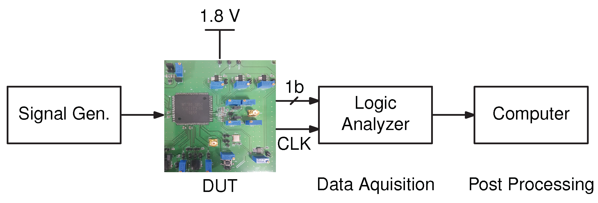
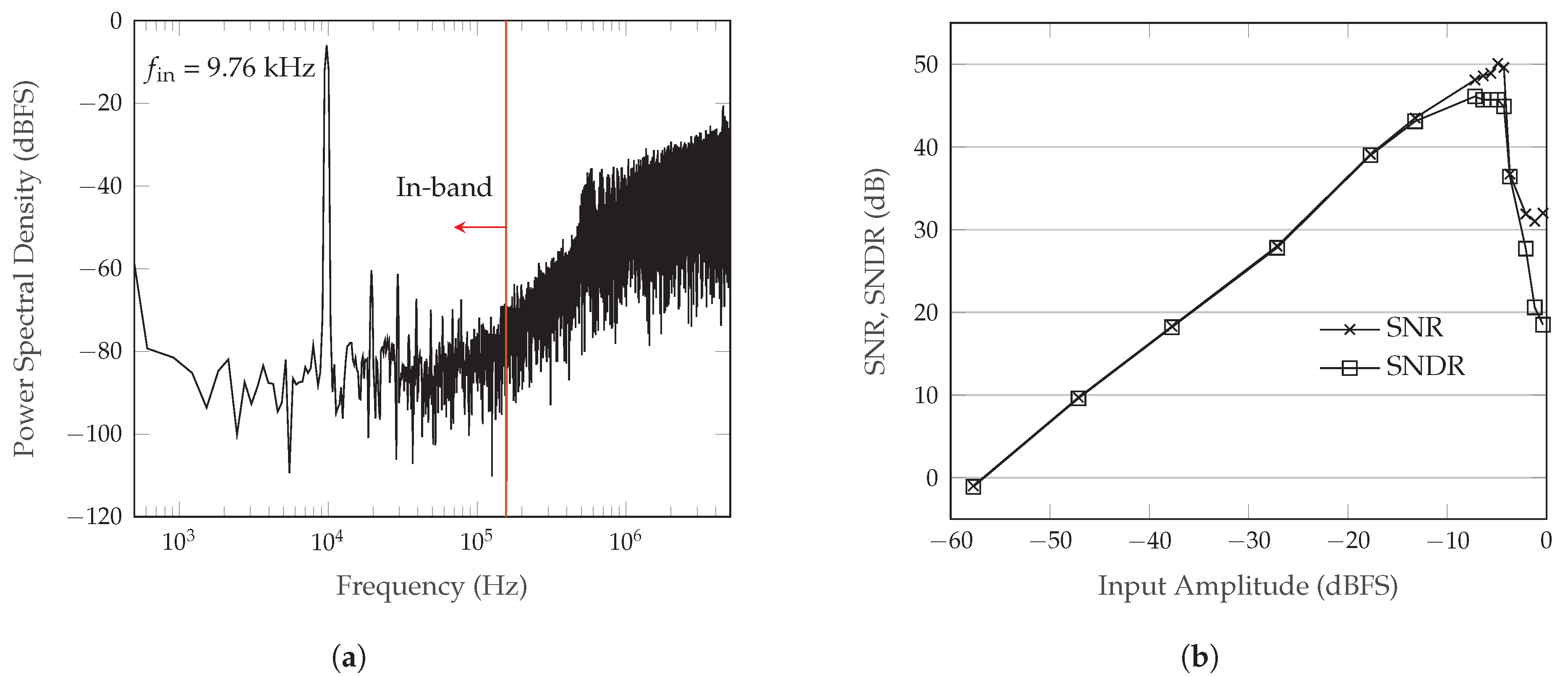
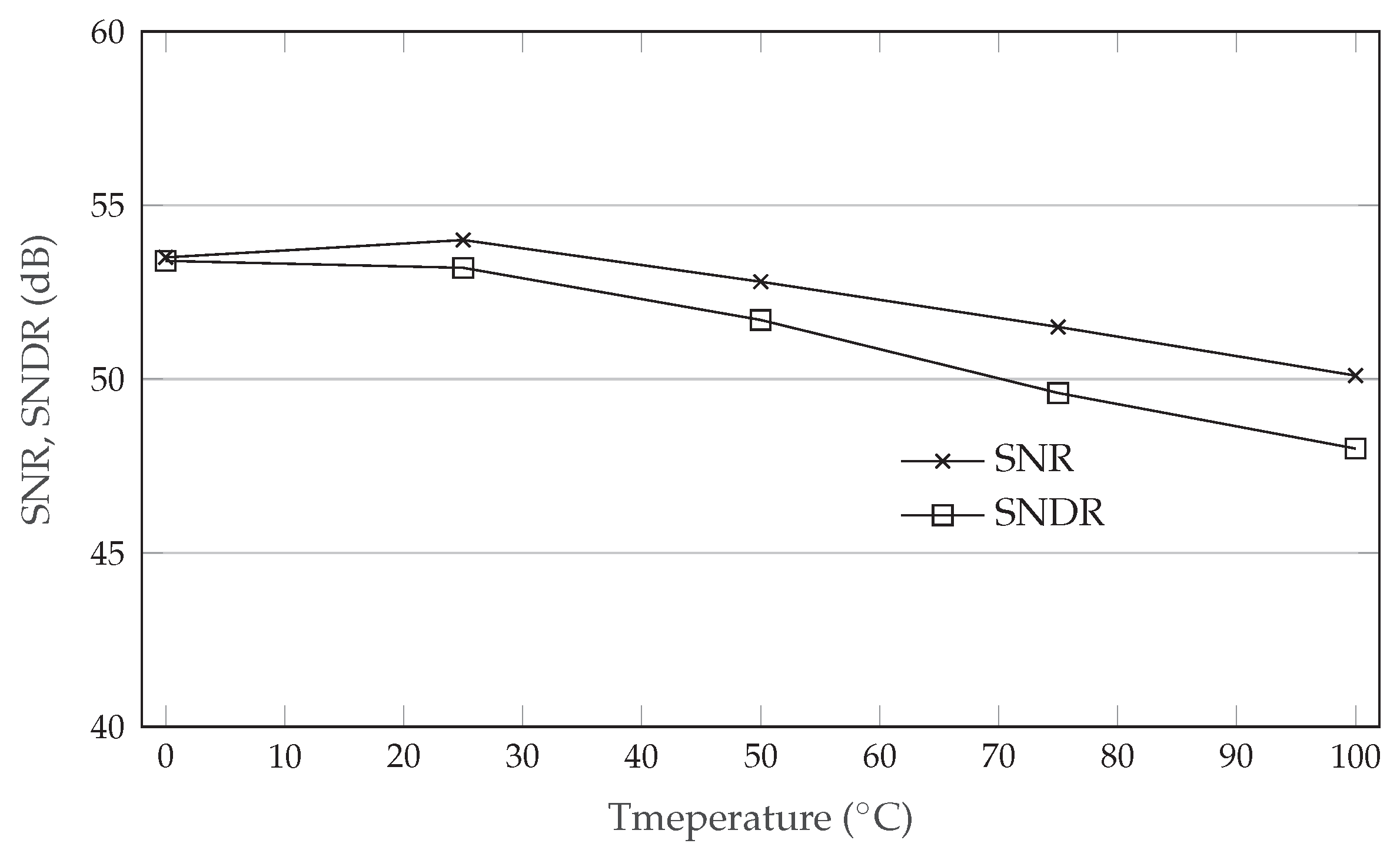
The fabricated chip was tested using the measurement setup shown in Figure 10. The PCB includes a single-ended-to-differential conversion circuit, reference voltage generators, and a crystal oscillator for the clock signal. Figure 11a shows the measured power spectral density of the modulator output with a 9.76-kHz 507-mVpp input signal, and Figure 11b shows signal-to-noise ratios (SNRs) and signal-to-noise-and-distortion ratios (SNDRs) for various input amplitudes. From the power spectral density, the second-order noise shaping is clearly seen. Unfortunately, high harmonic tones are also evident. These harmonic components are probably due to a couple of errors in the design: (1) the clock signals for bottom-plate sampling are connected in a wrong way, and (2) the fabricated modulator lacks reference buffers inside the chip. These errors are also believed to have raised the noise floor by about 3 dB. The second-order harmonic is probably due to the unbalanced reference voltages that are externally supplied to the chip. The mismatch between the pseudo-differential signal paths might have also contributed to the even-order harmonics. The measured peak SNR and SNDR are 50.1 dB and 46.3 dB, respectively. The dynamic range is about 56 dB. From process corner simulations, it is expected that the peak SNDR may drop by about 2.4 dB over the process variations. As suggested in Figure 12, the peak SNR and SNDR are also expected to deteriorate as the temperature increases.
The total power consumption is 684 µW from a 1.8-V supply voltage. Table 2 shows the power consumed in each sub-block. The most power-hungry blocks are integrators, and the clock generator also dissipates a considerable amount of power.
Table 3 summarizes the measured performance in comparison with related works. The figure-of- merit (FoM) of the fabricated modulator is not impressive owing to the aforementioned design errors and the rather high supply voltage. We redesigned the same modulator in 65-nm technology and its performance is also summarized in Table 3. With the lowered supply voltage and improved design, the power consumption is drastically reduced from 684 µW to 274 µW. Furthermore, the sampling frequency can be increased to 50 MHz without degradation of SNR or SNDR, resulting in better FoMs. Even if the SNDR discrepancy of about 5 dB is taken to account between schematic simulation and measurement, the proposed modulator is expected to achieve competitive performance.

4. Conclusions

ZCBI is an attractive alternative to the conventional power-hungry switched-capacitor integrator because the ZCD can be implemented using a simple inverter circuit and auto-zeroing techniques. However, ZCBI is prone to errors caused by the overshoot, and reducing the overshoot results in lower speed in general. In order to break the trade-off between speed and accuracy, a two-phase charging scheme is needed, but it is not straightforward to apply the conventional two-phase charging scheme to the inverter-based ZCD. This paper proposes the use of charge sharing to implement the two-phase charging scheme. The proposed technique is readily applicable to the inverter-based ZCD and is able to reduce the power consumption and the circuit complexity. The proposed charging scheme was applied to a second-order Δ Σ modulator designed in 0.18-µm CMOS technology. The modulator consists of two proposed ZCBIs, a 1-bit quantizer, a 1-bit DAC, and a clock generator. The ZCD for ZCBIs makes use of a dynamic buffer to reduce the delay. Measurement results show that the modulator achieves a 56-dB dynamic range and a 46.3-dB peak SNDR over a 156-kHz in-band bandwidth with a 684-µW power consumption. We also designed the modulator in 65-nm CMOS technology and simulation results suggest that the proposed modulator is likely to achieve better energy efficiency in advanced technology.

Author Contributions

Methodology, D.-J.M.; Supervision, J.H.S.; Writing—original draft preparation, D.-J.M. and J.H.S.

Funding

This work was supported by Nano-Material Technology Development Program through the National Research Foundation of Korea (NRF) funded by Ministry of Science and ICT (NRF-2017M3A7B4049517).

Acknowledgments

The chip fabrication and EDA tool were supported by the IC Design Education Center (IDEC), Korea.

Conflicts of Interest

The authors declare no conflict of interest.

Abbreviations

The following abbreviations are used in this manuscript:
OTAOperational Transconductance Amplifier
ZCBIZero-Crossing-Based Integrator
ZCDZero-Crossing Detector
ADCAnalog-to-Digital Converter
DACDigital-to-Analog Converter
CMOSComplementary Metal-Oxide-Semiconductor
OSROver-Sampling Ratio
SNRSignal-to-Noise Ratio
SNDRSignal-to-Noise-and-Distortion Ratio
FoMFigure of Merit

References

  1. Annema, A.-J.; Nauta, B.; van Langevelde, R.; Tuinhout, H. Analog circuits in ultra-deep-submicron CMOS. IEEE J. Solid-State Circuits 2005, 40, 132–143. [Google Scholar] [CrossRef] [Green Version]
  2. Murmann, B.; Nikaeen, P.; Connelly, D.J.; Dutton, R.W. Impact of Scaling on Analog Performance and Associated Modeling Needs. IEEE Trans. Electron. Devices 2006, 53, 2160–2167. [Google Scholar] [CrossRef]
  3. Chiu, Y.; Nikolic, B.; Gray, P.R. Scaling of analog-to-digital converters into ultra-deep-submicron CMOS. In Proceedings of the IEEE 2005 Custom Integrated Circuits Conference, San Jose, CA, USA, 18–21 September 2005; pp. 368–375. [Google Scholar] [CrossRef]
  4. Bult, K. Broadband communication circuits in pure digital deep sub-micron CMOS. In Proceedings of the 1999 IEEE International Solid-State Circuits Conference, Digest of Technical Papers, ISSCC, First Edition (Cat. No. 99CH36278), San Francisco, CA, USA, 17 February 1999; pp. 76–77. [Google Scholar] [CrossRef]
  5. Fiorenza, J.K.; Sepke, T.; Holloway, P.; Sodini, C.G.; Lee, H.-S. Comparator-Based Switched-Capacitor Circuits for Scaled CMOS Technologies. IEEE J. Solid-State Circuits 2006, 41, 2658–2668. [Google Scholar] [CrossRef]
  6. Mortazavi, S.Y.; Nabavi, A.; Amiri, P. High-accuracy Comparator-Based Switched-Capacitor structure. IEICE Electron. Expr. 2010, 7, 352–359. [Google Scholar] [CrossRef] [Green Version]
  7. Wulff, C.; Ytterdal, T. CBSC pipelined ADC with comparator preset, and comparator delay compensation. In Proceedings of the NORCHIP, Trondheim, Norway, 16–17 November 2009; pp. 1–4. [Google Scholar] [CrossRef]
  8. Brooks, L.; Lee, H.-S. A Zero-Crossing-Based 8-bit 200 MS/s Pipelined ADC. IEEE J. Solid-State Circuits 2007, 42, 2677–2687. [Google Scholar] [CrossRef]
  9. Musah, T.; Moon, U.-K. Pseudo-differential zero-crossing-based circuit with differential error suppression. In Proceedings of the 2010 IEEE International Symposium on Circuits and Systems, Paris, France, 30 May–2 June 2010; pp. 1731–1734. [Google Scholar] [CrossRef]
  10. Brooks, L.; Lee, H.-S. A 12b 50MS/s fully differential zero-crossing-based ADC without CMFB. In Proceedings of the 2009 IEEE International Solid-State Circuits Conference—Digest of Technical Papers, San Francisco, CA, USA, 8–12 February 2009; pp. 166–167. [Google Scholar] [CrossRef]
  11. Musah, T.; Kwon, S.; Lakdawala, H.; Soumyanath, K.; Moon, U.-K. A 630μW zero-crossing-based ΔΣ ADC using switched-resistor current sources in 45nm CMOS. In Proceedings of the 2009 IEEE Custom Integrated Circuits Conference, Rome, Italy, 13–16 September 2009; pp. 1–4. [Google Scholar] [CrossRef]
  12. Wong, K.-F.; Sin, S.-W.; U, S.-P.; Martins, R.P. A modified charging algorithm for comparator-based switched-capacitor circuits. In Proceedings of the 52nd IEEE International Midwest Symposium on Circuits and Systems, Cancun, Mexico, 2–5 August 2009; pp. 86–89. [Google Scholar] [CrossRef]
  13. Huang, M.-C.; Liu, S.-I. A Fully Differential Comparator-Based Switched-Capacitor ΔΣ Modulator. IEEE Trans. Circuits Syst. Express Briefs 2009, 56, 369–373. [Google Scholar] [CrossRef]
  14. Yamamoto, K.; Carusone, A. A 1-1-1-1 MASH Delta-Sigma Modulator With Dynamic Comparator-Based OTAs. IEEE J. Solid-State Circuits 2012, 47, 1866–1883. [Google Scholar] [CrossRef]
  15. Min, D.-J.; Choi, S.Y.; Shim, J.H. A Low-Power 2nd-Order Delta-Sigma ADC with an Inverter- Based Zero-Crossing Detector. In Proceedings of the 25th IEEE International Conference on Electronics, Circuits and Systems (ICECS), Bordeaux, France, 9–12 December 2018; pp. 817–820. [Google Scholar] [CrossRef]
  16. Chen, C.; Tan, Z.; Pertijs, M.A.P. A 1V 14b self-timed zero-crossing-based incremental ΔΣ ADC. In Proceedings of the 2013 IEEE International Solid-State Circuits Conference Digest of Technical Papers, San Francisco, CA, USA, 17–21 February 2013; pp. 274–275. [Google Scholar] [CrossRef]
  17. Silva, J.; Moon, U.; Steensgaard, J.; Temes, G.C. Wideband low-distortion delta-sigma ADC topology. Electron. Lett. 2001, 37, 737. [Google Scholar] [CrossRef]
  18. Wu, L.; Keskin, M.; Moon, U.; Temes, G. Efficient common-mode feedback circuits for pseudo-differential switched-capacitor stages. In Proceedings of the 2000 IEEE International Symposium on Circuits and Systems, Emerging Technologies for the 21st Century. Proceedings (IEEE Cat No.00CH36353), Geneva, Switzerland, 28–31 May 2000; pp. 445–448. [Google Scholar] [CrossRef]
  19. Pavan, S.; Krishnapura, N.; Pandarinathan, R.; Sankar, P. A Power Optimized Continuous-Time ΔΣ ADC for Audio Applications. IEEE J. Solid-State Circuits 2008, 43, 351–360. [Google Scholar] [CrossRef]
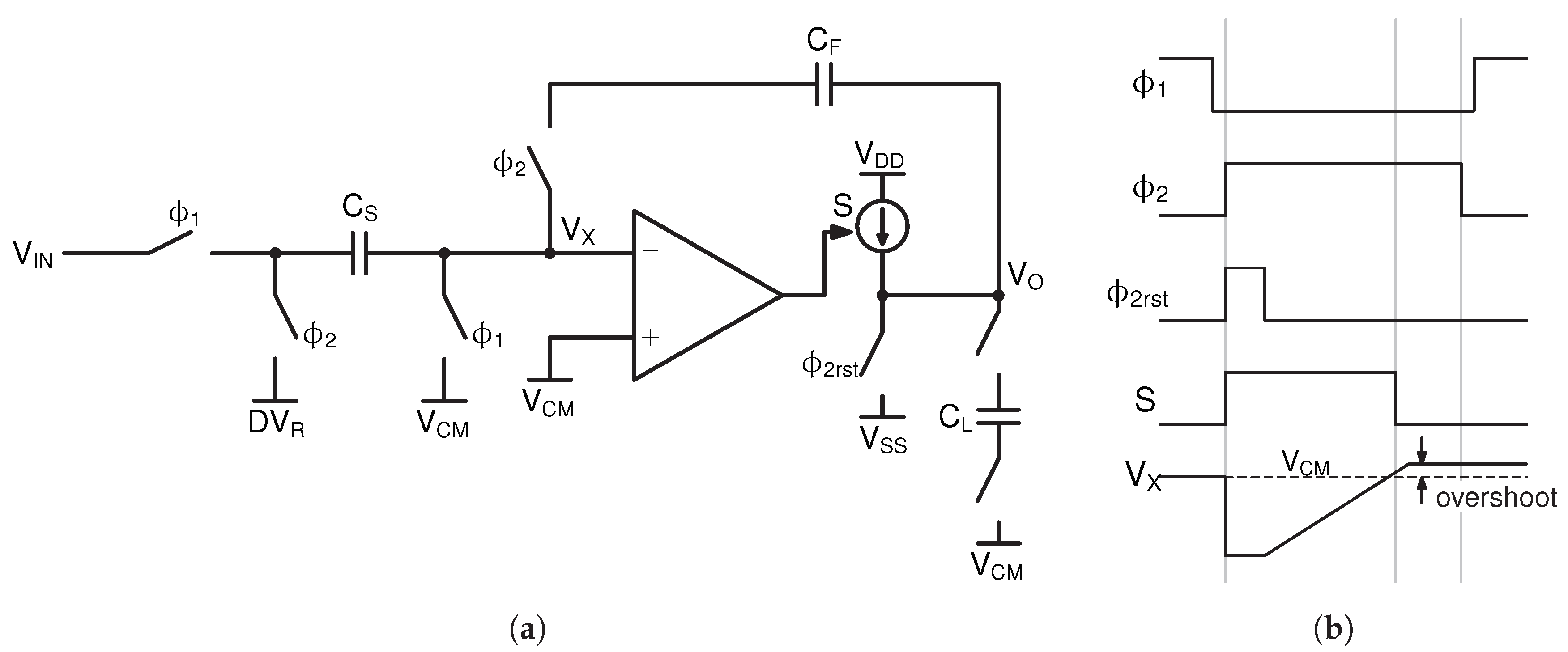
Figure 1. Conventional zero-crossing-based switched-capacitor circuit. (a) Schematic diagram. (b) Timing diagram.
Electronics 08 00821 g001
Figure 2. Two-phase charging schemes. (a) Bidirectional. (b) Unidirectional.
Electronics 08 00821 g002
Figure 3. A switched-capacitor circuit using an inverter-based zero-crossing-detectors (ZCD) [16].
Electronics 08 00821 g003
Figure 4. The inverter-based zero-crossing-based integrators (ZCBI) using a dynamic buffer. (a) Schematic diagram. (b) Timing diagram.
Electronics 08 00821 g004
Figure 5. The ZCBI employing the charge-sharing-based two-phase charging scheme. (a) Schematic diagram. (b) Normal operation. (c) Erroneous operation.
Electronics 08 00821 g005
Figure 6. The structure of the designed second-order Δ Σ modulator.
Electronics 08 00821 g006
Figure 7. Schematic diagram of the modulator.
Electronics 08 00821 g007
Figure 8. Chip micrograph. The core size is 650 µm × 460 µm.
Electronics 08 00821 g008
Figure 9. Distribution of V X | reset .
Electronics 08 00821 g009
Figure 10. Test setup.
Electronics 08 00821 g010
Figure 11. Measured results. (a) Power spectral density (# of fast Fourier transform (FFT) bins: 32768). (b) Signal-to-noise ratio (SNR) and signal-to-noise and distortion ratio (SNDR) versus input amplitudes.
Electronics 08 00821 g011
Figure 12. Simulated SNR and SNDR over temperature.
Electronics 08 00821 g012
Table 1. Summary of design.
Technology180-nm CMOS
Sampling Frequency10 MHz
V DD 1.8 V
V CM 0.9 V
D V R 0.4 V or 1.4 V
C S , 1 st , C S , 2 nd 25 fF
C F , 1 st , C F , 2 nd 50 fF, 100 fF
* C Ltot , 1 st , C Ltot , 2 nd 300 fF, 500 fF
* C S and C F are excluded.
Table 2. Power consumption breakdown.
Sub-BlockPower Consumption (µW)Percentage (%)
1st Integrator23534.3
2nd Integrator22933.5
Adder5.60.8
Quantizer5.70.8
DAC0.90.1
Clock Genrator15122.1
Ref. buffers, etc.56.88.4
Total684100
Table 3. Performance comparison with other work.
[11][13][14][16]This Work
Technology (nm)451806516018065 ( 1 ) 65 ( 1 )
Supply Voltage (V)1.11.81.21.01.81.21.2
Sampling Frequency (MHz)502.56400.014 ( 2 ) 101050
Oversampling Ratio306481323232
Bandwidth (kHz)8332025000.7156156781
Peak SNDR (dB)47.765.370.4N/A46.353.253.7
Peak SNR (dB)52.5N/AN/A81.850.156.356.5
Dynamic Range (dB)54.37171.3N/A56N/A56.5
Power Consumption (µW)630420373020684274312
FoM S ( 3 ) (dB)139142159157130140.8148
FoM W ( 4 ) (pJ/conv-step)1.916.980.2761.4813.22.350.5
( 1 ) Simulation results. Others are from measurements. ( 2 ) Self-timed incremental ADC. Translated from the longest conversion time. ( 3 ) FoM S = SNDR ( dB ) + 10 log 10 ( Bandwidth / Power ) . ( 4 ) FoM W = POWER / ( 2 ( SNDR 1.76 ) / 6.02 × 2 × Bandwidth ) .