Article

A New Low-Voltage Low-Power Dual-Mode VCII-Based SIMO Universal Filter

Department of Industrial and Information Engineering and Economics, University of L’Aquila, 67100 L’Aquila, Italy
*
Author to whom correspondence should be addressed.
Electronics 2019, 8(7), 765; https://doi.org/10.3390/electronics8070765
Submission received: 24 June 2019 / Revised: 3 July 2019 / Accepted: 4 July 2019 / Published: 9 July 2019
(This article belongs to the Special Issue Filter Design Solutions for RF systems)

Abstract

:
In this paper, a new low-voltage low-power dual-mode universal filter is presented. The proposed circuit is implemented using inverting current buffer (I-CB) and second-generation voltage conveyors (VCIIs) as active building blocks and five resistors and three capacitors as passive elements. The circuit is in single-input multiple-output (SIMO) structure and can produce second-order high-pass (HP), band-pass (BP), low-pass (LP), all-pass (AP), and band-stop (BS) transfer functions. The outputs are available as voltage signals at low impedance Z ports of the VCII. The HP, BP, AP, and BS outputs are also produced in the form of current signals at high impedance X ports of the VCIIs. In addition, the AP and BS outputs are also available in inverting type. The proposed circuit enjoys a dual-mode operation and, based on the application, the input signal can be either current or voltage. It is worth mentioning that the proposed filter does not require any component matching constraint and all sensitivities are low, moreover it can be easily cascadable. The simulation results using 0.18 μm CMOS technology parameters at a supply voltage of ±0.9 V are provided to support the presented theory.

1. Introduction

Filters are among the most widely used circuits in different areas such as instrumentation, communication, control, and signal processing systems [1,2,3,4,5]. Traditionally, filters were designed in voltage mode using active devices such as operational amplifiers (Op-Amp). However, due to the reduced supply voltage in advanced CMOS technologies and the ever-increasing demand on low-power circuits, the design of high-performance Op-Amp-based filters has become very difficult. The inherent low-voltage nature of current-mode signal processing has motivated a wide investigation on current-mode filters with the aim of achieving better results under low supply voltage restrictions. Among the various types of current-mode filters, the multifunction or universal type which is able to produce several transfer functions simultaneously with the same circuit, is good solution for the ever-increasing demand of the market for low-power circuits. That is why, in recent years, numerous current-mode universal filters have appeared in literature [6,7,8,9,10,11,12].
In the universal filter category, second-order (biquadratic) filters play an important role in the field of analog signal processing such as the implementation of phase-locked loop (PLL), frequency modulation (FM), stereo demodulation, etc. [1,2,3,4,5]. They can be classified in single-input-multiple-output (SIMO), multiple-input-single-output (MISO), and multiple-input-multiple-output (MIMO) topologies. A deep investigation in the literature reveals that various current-mode active building blocks such as four-terminal floating nullor (FTFN) [6], differential voltage current conveyor (DVCC) [7], current-controlled current conveyor transconductance amplifier (CCCCTA) [7], current feedback operational amplifier (CFOA) [9], current differencing buffered amplifier (CDBA) [10,11], modified current-controlled current differencing transconductance amplifier (MCCCDTA) [12], operational transconductance amplifier (OTA) [13] LT1228 IC [14], fully differential second-generation current conveyor [15], current follower cascaded transconductance amplifier (CFCTA) [16], and voltage differencing differential difference amplifier [17] have been used in the design of multifunction filters. The common feature of the multifunction filters of [6,7,8,12] is that their output signal is in the form of a current. The reason is that the used current-mode active building blocks lack a low-impedance voltage output port. Therefore, for applications requiring voltage outputs, these circuits require additional voltage buffers resulting in higher power consumption and chip area. There are a few current-mode building blocks such as CDBA, CFOA, and FTFN that have low-impedance voltage output ports. However, the voltage output multifunction filters based on these active building blocks reported in [6,9,10,11] suffer from serious drawbacks, the most serious of them being their inability to provide low impedance at all voltage output ports and the consequent requirement of additional voltage buffers. For example, the voltage output multifunction FTFN-based filter of [6] requires an extra voltage buffer at its LP output. Similarly, the multifunction CFOA-based filter of [9] requires an extra voltage buffer for HP output. Although the CDBA-based multifunction filter of [9] provides low impedance for all voltage outputs, it has the load and other passive elements connected to output ports, so the output ports must be designed to have high current drive capability. These will result in a complicated internal circuit for the used CDBA. The filter circuits of [14,15,16,17,18] suffer from a high supply voltage requirement.
Recently a new active building block called the second-generation voltage conveyor (VCII) has attracted the attention of researchers [19,20]. It is the dual of well-known second-generation current conveyor (CCII) and, compared to other active building blocks, enjoys a simple internal structure and features more design flexibility. It is characterized by a low-impedance current input port, a high-impedance current output port and a low-impedance voltage output port. Using the low-impedance current input port, current summing/subtracting operations can be performed very easily. In addition, having a low-impedance voltage output port makes this building block highly suitable for voltage output applications. In other words, the low-impedance voltage output port makes the extra voltage buffer unnecessary. More interestingly, VCII internal structure is composed of a current buffer and a voltage buffer. This simple implementation results in low power consumption and low chip area.
Despite these attractive features, up to now, VCII is not used in the implementation of universal filters. Therefore, in this paper, we take the advantages offered by the VCII block to design a voltage output low-power second-order universal filter. The presented filter topology employs one inverting current buffer (I-CB), three double output VCIIs, five resistors, and three capacitors. I-CB is simply a current buffer with gain of −1. The proposed universal filter is designed in SIMO topology and provides all-pass (AP), band-pass (BP), band-stop (BS), low pass (LP), and high-pass (HP) functions. All the outputs are available in voltage form at the low-impedance voltage output ports of the VCII. Interestingly, the HP, BP, and BS outputs are also available in current form at the high-impedance port of the VCII. Moreover, the AP and BS outputs are provided in both the inverting and non-inverting types. The proposed circuit is in dual mode and, based on the application, the input signal can be either a current or a voltage.
The organization of this paper is as follows. In Section 2 the VCII block and its implementation are presented. In Section 3, the proposed filter topology is given. In Section 4, the non-ideal analysis is performed. The simulation results and a comparative table are presented in Section 5. Finally, Section 6 concludes the paper.

2. The VCII Internal Circuit Design

Figure 1a,b shows the schematic diagram and the symbolic representation of a dual-output VCII, respectively. It has a low-impedance current input Y port. Ideally, the impedance at the Y terminal is zero. The current applied to the Y port is transferred to the X1 and X2 ports with a current gain of AI1 and AI2, respectively. In the ideal case, the values of AI1 and AI2 are unity. X1 and X2 are high-impedance (ideally ∞) current output ports. The voltage produced at the X1 and X2 ports is conveyed to the Z1 and Z2 ports, respectively. The voltage gain between X1–Z1 and X2–Z2 is shown by AV1 and AV2, respectively, which are equal to unity in the ideal case. The Z1 and Z2 ports are low-impedance (ideally zero) voltage output ports. The relation between the port currents and voltages is:
v Y = r Y i Y , i X 1 = A I 1 i Y , i X 2 = A I 2 i Y , V Z 1 = A V 1 V X 1 , V Z 2 = A V 2 V X 1 .
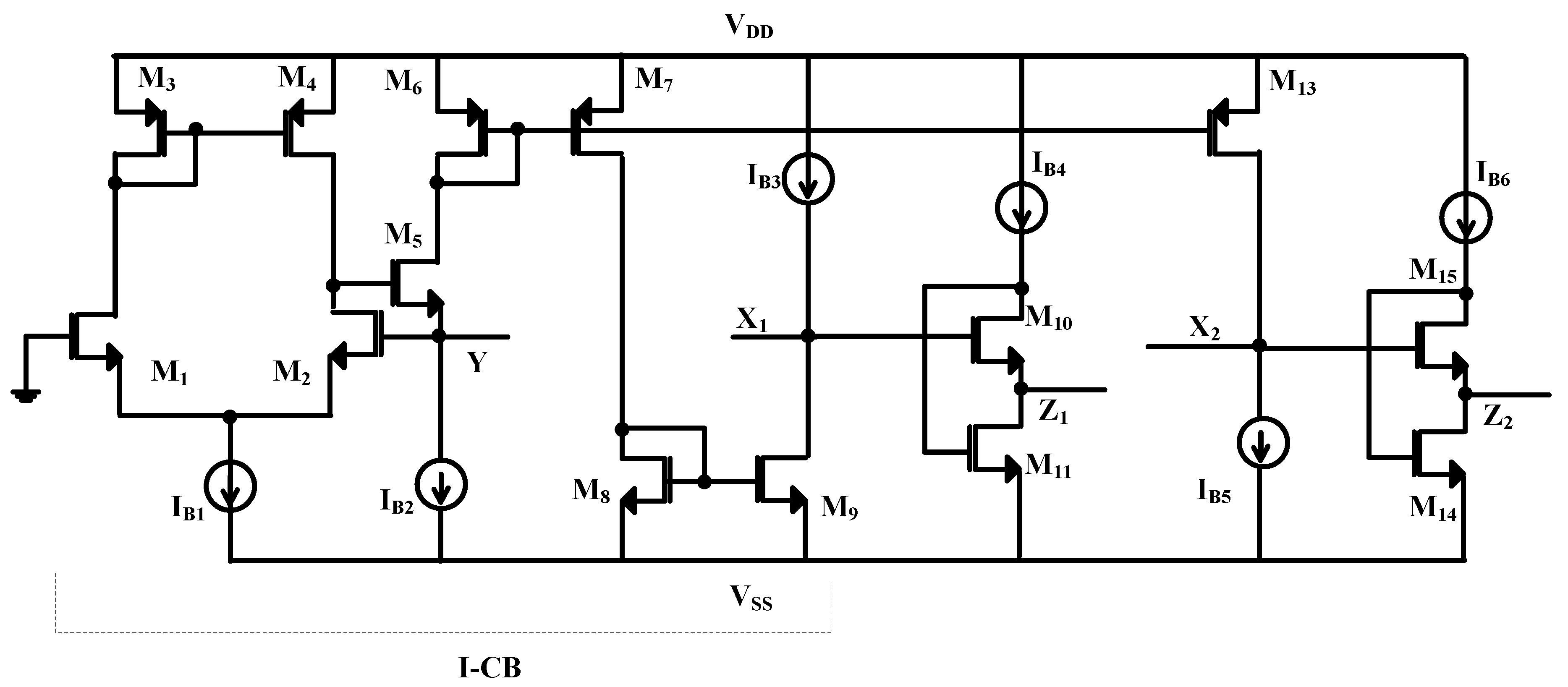
As seen from Figure 1, a dual-output VCII is composed of a dual-output current buffer and two voltage buffers. Figure 2 shows the CMOS circuit implementation of the dual-output VCII, representing the dual-output version of the VCII circuit reported in [19]. The current buffers are composed by M1M9, M13 transistors together with current sources IB1IB3, IB5. The input current to the Y terminal is transferred to the X1 terminal with a current gain of about −1 by an inverting current buffer (I-CB) made of M1M9 transistors and IB1IB3 current sources. The non-inverting current buffer made of M1M6, M13 and current sources IB1IB2, IB4 conveys the input current of the Y terminal to the X2 terminal with a current gain of about +1. The voltage buffers are simply two flipped voltage followers (FVFs) [21] formed by M10M11, M14M15 transistors and current sources IB4, IB6. The used FVFs provide very low impedance at the Z terminals. The negative-feedback loop established by M1M5 provides very low impedance at the Y terminal. The main feature of the proposed circuit is very low impedance at the Y terminal, which makes this node ideal for a current summing operation. In addition, very low impedance at the Y terminal ensures negligible voltage drop at this node.

3. The Proposed Universal Filter

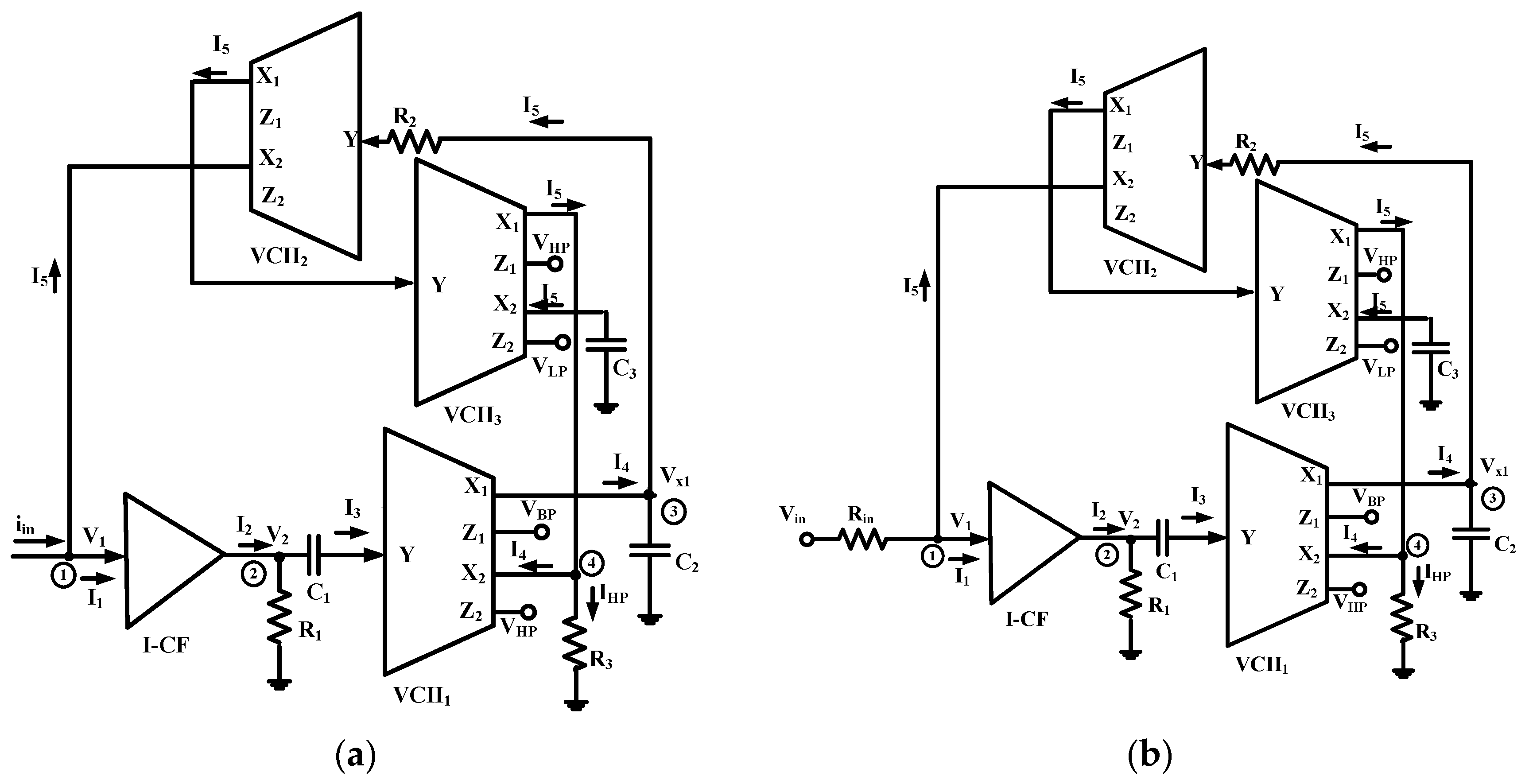
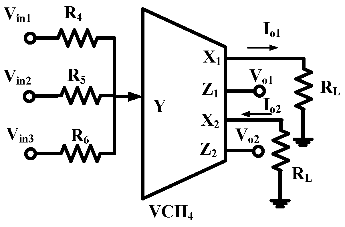
The proposed VCII-based filter topology is shown in Figure 3. It is based on three dual-output VCIIs and one I-CB as active building blocks and three resistors and three capacitors as passive elements. There is only one floating capacitor. The input signal can be either current or voltage type. Input current is applied to the circuit directly as shown in Figure 3a, while, due to the very low impedance at the Y terminal which is ideally zero, voltage signals can only be applied through a resistor as shown in Figure 3b. The circuit is designed in single-input three-output topology and produces second-order HP, LP, and BP outputs simultaneously. The outputs are available as voltage signals at the low-impedance Z ports of VCII. The HP output can also be provided in the form of current at the high-impedance X2 port of the VCII. The AP and BS outputs can be simply produced using an additional VCII block and three resistors as shown in Figure 4 in which, as it will be shown, Vin1, Vin2, and Vin3 are connected to HP, LP, and BP outputs, respectively. The transfer functions of Figure 3a and b are similar except that, for Figure 3b, the input signal should be replaced with Vin/Rin. For this similarity, in the following analysis, the transfer functions are only derived for the topology of Figure 3a.
Due to the very low impedance at the Y port of the VCII, which is ideally zero, we can assume this port at ground. Therefore, applying Kirchoff’s Current Law (KCL) analysis at node 2, gives I3 as:
I 3 = s C 1 R 1 1 + s C 1 R 1 I 2 .
Using Equation (1), the relationship between I1I2 and I3I4 can be expressed as:
I 1 I 2 ;   I 3 I 4
By assuming the Y port of VCII2 at ground and performing a KCL analysis at node 3, I5 is obtained as:
I 5 = 1 1 + s C 2 R 2 I 4 .
At the input node (node 1) we have:
i i n = I 1 + I 5 .
Using Equations (3) and (5), I2 is found as:
I 2 = ( 1 + s C 1 R 1 ) ( 1 + s C 2 R 2 ) s 2 C 1 C 2 R 1 R 2 + s ( 2 C 1 R 1 + C 2 R 2 ) + 1 i i n .
For VX1 (the voltage at node 3) we have:
V X 1 = R 2 1 + s C 2 R 2 I 4 .
From Equations (2), (3), and (6), I4 is obtained as:
I 4 = s C 1 R 1 ( 1 + s C 2 R 2 ) s 2 C 1 C 2 R 1 R 2 + s ( 2 C 1 R 1 + C 2 R 2 ) + 1 i i n .
Inserting Equation (8) into Equation (7), gives VX1 as:
V X 1 = V Z 1 = V B P = s C 1 R 1 R 2 s 2 C 1 C 2 R 1 R 2 + s ( 2 C 1 R 1 + C 2 R 2 ) + 1 i i n .
Equation (9) represents a second-order BP response. Due to the voltage buffer action between X1 and Z1 terminals, the BP response is available at the Z1 port as a voltage signal.
From Equations (4) and (8), I5 is found as:
I 5 = s C 1 R 1 s 2 C 1 C 2 R 1 R 2 + s ( 2 C 1 R 1 + C 2 R 2 ) + 1 i i n .
By subtracting I4 (Equation (8)) from I5 (Equation (10)) the HP output can be provided:
I H P = I 5 I 4 = s 2 C 1 R 1 C 2 R 2 s 2 C 1 C 2 R 1 R 2 + s ( 2 C 1 R 1 + C 2 R 2 ) + 1 i i n .
As in Figure 3a, by connecting the current output X2 ports of VCII1 and VCII3, a HP output in the form of current is produced at node 4. The HP output is also available in the form of voltage at Z2 ports of VCII1 and VCII3 as:
V H P = R 3 I H P = s 2 C 1 R 1 C 2 R 2 R 3 s 2 C 1 C 2 R 1 R 2 + s ( 2 C 1 R 1 + C 2 R 2 ) + 1 i i n .
Using Equation (10), the voltage at X2 and Z2 ports of VCII3 have a LP transfer function as:
V X 2 V Z 2 = I 5 s C 3 = V L P = C 1 R 1 C 3 s 2 C 1 C 2 R 1 R 2 + s ( 2 C 1 R 1 + C 2 R 2 ) + 1 i i n .
By assuming the Y terminal of VCII4 at ground, the Io1 and Io2 outputs are achived as:
| I o 1 | = | I o 2 | = V i n 1 R 4 + V i n 2 R 5 + V i n 3 R 6 .
For the AP output, Vin1, Vin2, and Vin3 are connected to VHP, VBP, and VLP outputs, respectively. Therefore, by inserting VHP (Equation (12)), VBP (Equation (9)), and VLP (Equation (13)) into Equation (14), the AP transfer function is achieved as:
I A P = I o 1 = I o 2 = s 2 C 1 R 1 C 2 R 2 R 3 R 4 s C 1 R 1 R 2 R 5 + C 1 R 1 C 3 R 6 s 2 C 1 C 2 R 1 R 2 + s ( 2 C 1 R 1 + C 2 R 2 ) + 1 I i n .
For the BS output, Vin2 is connected to ground while Vin1 and Vin3 are connected to VHP and VLP outputs respectively giving:
I B S = I o 1 = I o 2 = s 2 C 1 R 1 C 2 R 2 R 3 R 4 + C 1 R 1 C 3 R 6 s 2 C 1 C 2 R 1 R 2 + s ( 2 C 1 R 1 + C 2 R 2 ) + 1 I i n .
Therefore, the tAP and BS outputs are produced as current signals at the X1 and X2 terminals of VCII4. In addition, as shown in Figure 4, both AP and BS outputs are available as voltage signals at the Z1 and Z2 terminals of VCII4 in inverting and non-inverting forms, respectively.
From Equation (9) the quality factor Q and natural frequency ω0 are determined using the following formulas:
ω 0 = 1 C 1 C 2 R 1 R 2 .
Q = C 1 C 2 R 1 R 2 2 C 1 R 1 + C 2 R 2 .
By assuming R1 = R2 = R and C1 = C2 = C in Equations (17) and (18), we have:
ω 0 = 1 R C .
Q = 1 3 .
Therefore, ω0 can be set by R and C independent of Q.
The sensitivities of the proposed filter are calculated using the well-known definition of sensitivity in Equation (15) [22] as:
S x F = x F F x .
S R 1 ω 0 = S R 2 ω 0 = S C 1 ω 0 = S C 2 ω 0 = 1 2 .
S C 1 Q = S R 1 Q = [ 1 2 2 R 1 C 1 ( 2 C 1 R 1 + C 2 R 2 ) ] .
S C 2 Q = S R 2 Q = [ 1 2 R 2 C 2 ( 2 C 1 R 1 + C 2 R 2 ) ] .
For C1 = C2 = C, R1 = R2 = R, from Equations (23) and (24), we have:
S C 1 Q = S R 1 Q = [ 1 2 2 3 ] = 1 6 .
S C 2 Q = S R 2 Q = [ 1 2 1 3 ] = 1 6 .
As seen from Equations (22), (25), and (26), the proposed filter exhibits reduced sensitivities to passive parameters.

4. Non-Ideal Analysis

The non-ideal analysis of the proposed universal filter can be performed by considering the non-ideal current and voltage gains of the used VCIIs. Using Equation (1), we have:
I 2 = A I B I 1 ;   I 4 = A I 1 I 3
where AIB and AI1 are the gain of the current buffer and the current gain of VCII1 at its X1 terminal, respectively.
At the input node (node 1) we have:
i i n = I 1 + A I 2 I 5 ,
where A’I2 is the current gain of VCII2 at its X2 terminal.
Using Equations (27) and (28) and Equations (2) and (4), I2 is found as:
I 2 = A I B ( 1 + s C 1 R 1 ) ( 1 + s C 2 R 2 ) s 2 C 1 C 2 R 1 R 2 + s ( C 1 R 1 { 1 + A I 2 A I 1 A I B } + C 2 R 2 ) + 1 i i n .
From Equations (27) and (29), I5 is obtained as:
I 5 = A I B A I 1 s C 1 R 1 s 2 C 1 C 2 R 1 R 2 + s ( C 1 R 1 { 1 + A I 2 A I 1 A I B } + C 2 R 2 ) + 1 i i n .
VLP can be expressed as:
V L P = V Z 23 = A V 2 V X 23 = A I 2 A V 2 1 s C 3 I 5 ,
where VZ23 and VX23 are the voltages at the Z2 and X2 terminals of VCII3, respectively. A”V2 is the voltage gain at the Z2 terminal of VCII3. Inserting Equation (30) into Equation (31), VLP is found as:
V L P = A I 2 A V 2 A I B A I 1 C 1 R 1 C 3 s 2 C 1 C 2 R 1 R 2 + s ( C 1 R 1 { 1 + A I 2 A I 1 A I B } + C 2 R 2 ) + 1 i i n .
From Equations (2) and (28), I4 is found as:
I 4 = A I B A I 1 s C 1 R 1 ( 1 + s C 2 R 2 ) s 2 C 1 C 2 R 1 R 2 + s ( C 1 R 1 { 1 + A I 2 A I 1 A I B } + C 2 R 2 ) + 1 i i n .
Inserting Equations (30) and (33) into Equation (11) gives IHP as:
I H P = A I B A I 1 s 2 C 1 R 1 C 2 R 2 s 2 C 1 C 2 R 1 R 2 + s ( C 1 R 1 { 1 + A I 2 A I 1 A I B } + C 2 R 2 ) + 1 i i n .
From Equation (34), VHP1 and VHP2 are found as:
V H P 1 = A I B A I 1 A V 2 s 2 C 1 R 1 C 2 R 2 R 3 s 2 C 1 C 2 R 1 R 2 + s ( C 1 R 1 { 1 + A I 2 A I 1 A I B } + C 2 R 2 ) + 1 i i n .
V H P 2 = A I B A I 1 A V 2 s 2 C 1 R 1 C 2 R 2 R 3 s 2 C 1 C 2 R 1 R 2 + s ( C 1 R 1 { 1 + A I 2 A I 1 A I B } + C 2 R 2 ) + 1 i i n .
Using Equations (33), (7), and (1), VBP is found as:
V B P = A I B A I 1 A V 1 s C 1 R 1 s 2 C 1 C 2 R 1 R 2 + s ( C 1 R 1 { 1 + A I 2 A I 1 A I B } + C 2 R 2 ) + 1 i i n ,
where Av1 is the voltage gain at the X1 terminal of VCII1. From Equation (37), the quality factor Q and the natural frequency ω0 are determined using the following formulas:
ω 0 = 1 C 1 C 2 R 1 R 2 .
Q = C 1 C 2 R 1 R 2 ( C 1 R 1 { 1 + A I 2 A I 1 A I B } + C 2 R 2 ) .
As seen from Equations (38) and (39), ω0 is not affected by the non-ideal gains of VCIIs. In addition, as current and voltage gains of VCIIs are designed to be very close to unity, their effect on Q is also negligible. The relations for AP and BS outputs can be simply achieved by inserting Equation (32) and Equations (35)–(37) into Equation (14).

5. Simulation Results and Comparative Analysis

The proposed multifunction filter of Figure 3 has been simulated with PSpice and using 0.18 μm CMOS parameters under a supply voltage of ±0.9 V. The circuit of Figure 2 is used as a VCII. For I-CB, the current buffer section of Figure 2, consisting of transistors M1M9 and current sources IB1IB3, is used. The chosen transistor aspect ratios are shown in Table 1. The values of bias currents are IB1 = 50 µA, IB2 = IB3 = IB4 = IB5 = IB6 = 20 µA. The values of the passive components are: R1 = R2 = 10 KΩ, C1 = C2 = 10 pF. The values of R3 and RL are 5 KΩ.
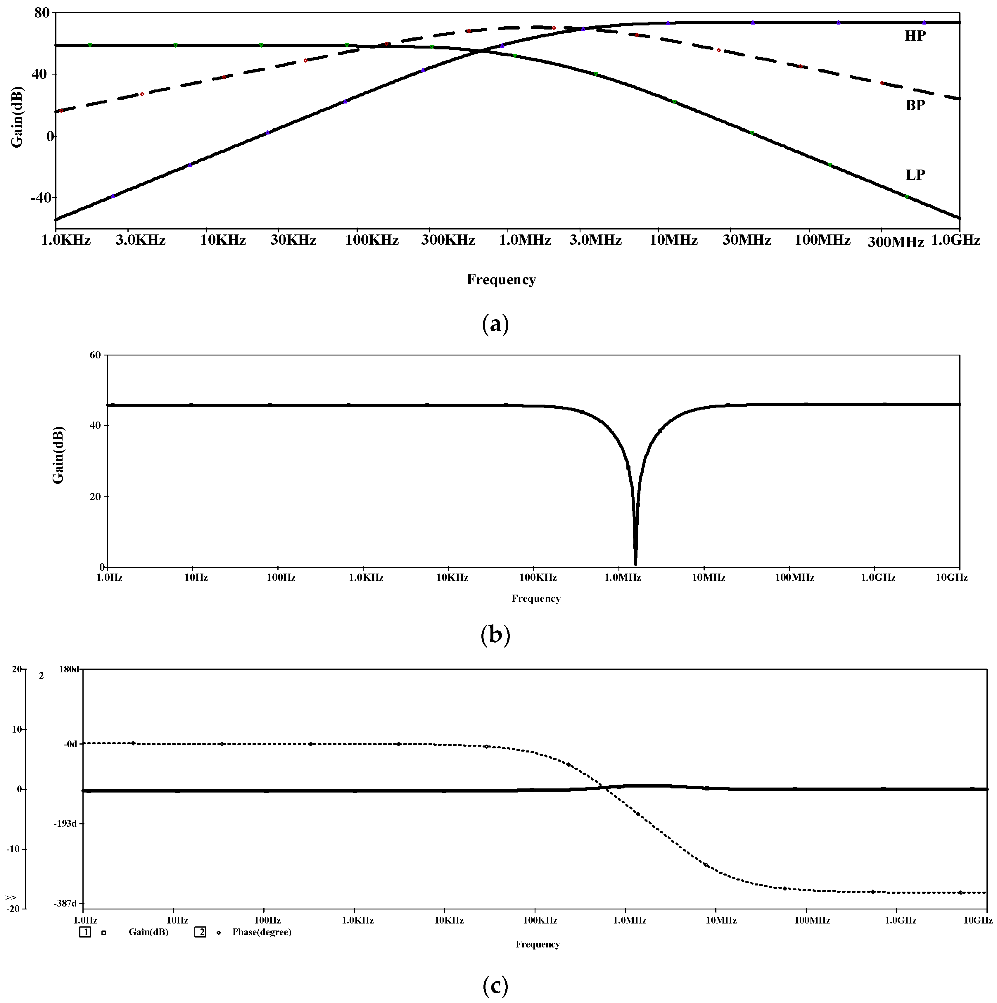
Figure 5a shows the frequency performances of the BP, HP, and LP outputs. The value of ω0 and Q is measured as 1.55 MHz and 0.33, respectively. From Equations (17) and (18), the values of ω0 and Q are calculated as 1.6 MHz and 0.33, respectively. As seen, there is a good agreement between theory and simulation results. The transient response of the different outputs is evaluated by applying a sinusoidal input current with a peak-to-peak value of 10 μA and frequency of 1.5 MHz. The total harmonic distortion (THD) values are 3.7%, 2.6%, and 3.6%, for HP, BP, and LP outputs, respectively.
Figure 5b shows the BS output, which is achieved by setting R4 = 12.5 KΩ, R5 = 78 kΩ, and R6 = 5 KΩ and connecting Vin1 = VHP, Vin2 = 0 and Vin3 = VLP. Figure 5c shows the gain and phase response of the AP output, which is achieved by connecting Vin1 = VHP, Vin2 = VBP and Vin3 = VLP and using the same values for R4R6.
The tunability of the proposed filter is investigated by varying the center frequency ω0, through C1 and C2. As shown in Figure 6, ω0 varies from 1 to 32 MHz for different values of capacitors without affecting Q.
The transient response of the different outputs is evaluated by applying a sinusoidal input current with a peak-to-peak value of 10 μA and a frequency of 1.5 MHz. The THD values are 2%, 1%, 6%, 1.4%, and 2% for the HP, BP, LP, AP, and BS outputs, respectively.
To investigate the circuit performance against transistor parameter tolerances, the circuit is simulated by applying 3% and 5% tolerance in VTH and β (with usual meaning of symbols) of transistors. The result is shown in Table 2, which acknowledges the negligible effect of tolerances in the circuit performance. The input impedance of the proposed filter is only 47 Ω and the output impedances for voltage outputs and current outputs are 93 Ω and 254 KΩ, respectively. The power consumption is also 1.47 µW.
A comparison between the proposed universal filter and some other previously reported works is drawn in Table 3. As seen, the proposed circuit is the only one providing both inverting and non-inverting type AP and BS outputs in current and voltage forms. The proposed circuit is also the only one that can produce all possible outputs as current and voltage signals in low-impedance and high-impedance terminals, respectively. It also enjoys low-voltage operation. Although the circuit proposed in [7] does not employ floating capacitors, it requires three extra current buffers at the input. In addition, compared to the previously published universal filters of [6,11,14,15,16,17], which employ two floating capacitors, there is only one floating capacitor in the proposed circuit. Compared to [9,16,17], the proposed circuit does not require extra current and/or voltage buffers at the input and output terminals.

6. Conclusions

In this paper a new VCII-based multifunction filter was presented. It was demonstrated that, taking advantage from one current buffer and four second-generation voltage conveyors (VCII) as active building blocks, it can perform BP, HP, LP AP, and BS filtering actions simultaneously maintaining a very low circuit complexity as well as a low static power consumption. It was shown that, the versatility of the VCII block allows us to produce outputs in forms of both current and voltage signals. Filter functionality was also acknowledged through simulations, which showed a good agreement with the presented theory. The robustness of the circuit against fabrication mismatches was analyzed and a final comparison between the presented work and the available literature was given.

Author Contributions

L.S. designed the circuit and wrote the paper; G.B. performed the simulations; G.F. and V.S. have analyzed the equations and edited the paper.

Funding

This research received no external funding.

Conflicts of Interest

The authors declare no conflict of interest.

References

  1. Alexander, C.; Sadiku, M. Fundamental of Electric Circuits, 2nd ed.; McGraw-Hill: New York, NY, USA, 2004. [Google Scholar]
  2. Ibrahim, M.; Minaei, S.; Kuntman, H. A 22.5 MHz current-mode KHN-biquad using differential voltage current conveyor and grounded passive elements. AEU Int. J. Electron. Commun. 2005, 59, 311–318. [Google Scholar] [CrossRef]
  3. Stornelli, V.; Pantoli, L.; Leuzzi, G.; Ferri, G. Fully differential DDA-based fifth and seventh order Bessel low pass filters and buffers for DCR radio systems. Analog Integr. Circuits Signal Process. 2013, 75, 305–310. [Google Scholar] [CrossRef]
  4. Alzaher, H.; Al-Ghamdi, M.; Ismail, M. CMOS low-power bandpass IF filter for Bluetooth. IET Circuits Devices Syst. 2007, 1, 7–12. [Google Scholar] [CrossRef]
  5. Prommee, P.; Saising, E. CMOS-based high-order LP and BP filters using biquad functions. IET Circuits Devices Syst. 2018, 12, 326–334. [Google Scholar] [CrossRef]
  6. Shah, N.; Malik, M. High impedance voltage- and current-mode multifunction filters. AEU Int. J. Electron. Commun. 2005, 59, 262–266. [Google Scholar] [CrossRef]
  7. Chen, H. Tunable versatile current-mode universal filter based on plus-type DVCCs. AEU Int. J. Electron. Commun. 2012, 66, 332–339. [Google Scholar] [CrossRef]
  8. Singh, S.; Maheshwari, S.; Mohan, J.; Chauhan, D. Electronically Tunable Current-Mode Universal Biquad Filter Based on the CCCCTA. In Proceedings of the International Conference on Advances in Recent Technologies in Communication and Computing, Kottayam, India, 27–28 October 2009; pp. 424–429. [Google Scholar]
  9. Horng, J.; Hou, C.; Huang, W.; Yang, D. Voltage/Current-Mode Multifunction Filters Using One Current Feedback Amplifier and Grounded Capacitors. Circuits Syst. 2011, 2, 60–64. [Google Scholar] [CrossRef] [Green Version]
  10. Arora, T.; Rana, U. Multifunction Filter Employing Current Differencing Buffered Amplifier. Circuits Syst. 2016, 7, 543–550. [Google Scholar] [CrossRef] [Green Version]
  11. Sagbas, M.; Koksal, M. A New Multi-mode Multifunction Filter Using CDBA. In Proceedings of the European Conference on Circuit Theory and Design, Cork, Ireland, 28 August–2 September 2005. [Google Scholar]
  12. Kumngern, M. Current-Mode Multifunction Biquadratic Filter Using a Single MCCCDTA. In Proceedings of the IEEE International Conference on Cyber Technology in Automation, Control, and Intelligent Systems (CYBER), Bangkok, Thailand, 27–31 May 2012; pp. 115–118. [Google Scholar]
  13. Kamat, D.; Ananda Mohan, P.; Gopalakrishna Prabhu, K. Current-mode operational transconductance amplifier-capacitor biquad filter structures based on Tarmy–Ghausi active-RC filter and second-order digital all-pass filters. IET Circuits Devices Syst. 2010, 4, 346–364. [Google Scholar] [CrossRef]
  14. Klungtong, S.; Thanapatay, D.; Jaikla, W. Three-Input Single-Output Voltage-Mode Multifunction Filter with Electronic Controllability Based on Single Commercially Available IC. Act. Passiv. Electron. Compon. 2017, 2017, 5240751. [Google Scholar] [CrossRef]
  15. Kumngern, M.; Supavarasuwat, P. A Voltage-Mode Three-Input One-Output Multifunction Filter Using Single FDCCII. In Proceedings of the 20th Asia-Pacific Conference on Communication (APCC2014), Pattaya, Thailand, 1–3 October 2014. [Google Scholar]
  16. Chanapromma, C.; Jaikla, W.; Chaichana, A. New Realization of Single CFCTA-Based Voltage-Mode Multifunction Filter. In Proceedings of the 3rd International Conference on Control and Robotics Engineering, Nagoya, Japan, 20–23 April 2018. [Google Scholar]
  17. Chaichana, A.; Sangyaem, S.; Jaikla, W. Multifunction Voltage-Mode Filter Using Single Voltage Differencing Differential Difference Amplifier. MATEC Web Conf. 2017, 95, 14003. [Google Scholar] [CrossRef] [Green Version]
  18. Ferri, G.; Stornelli, V. A 0.18 µm CMOS DDCCII for Portable LV-LP Filters. Radioengineering 2013, 22, 434–439. [Google Scholar]
  19. Safari, L.; Barile, G.; Ferri, G.; Stornelli, V. High performance voltage output filter realizations using second generation voltage conveyor. Int. J. RF Microw. Comput.-Aided Eng. 2018, 28, e21534. [Google Scholar] [CrossRef]
  20. Safari, L.; Barile, G.; Stornelli, V.; Ferri, G. An Overview on the Second Generation Voltage Conveyor: Features, Design and Applications. IEEE Trans. Circuits Syst. II Express Briefs 2018, 66, 547–551. [Google Scholar] [CrossRef]
  21. Carvajal, R.; Ramirez-Angulo, J.; Lopez-Martin, A.; Torralba, A.; Galan, J.; Carlosena, A.; Chavero, F. The flipped voltage follower: A useful cell for low-voltage low-power circuit design. IEEE Trans. Circuits Syst. I Regul. Pap. 2005, 52, 1276–1291. [Google Scholar] [CrossRef]
  22. Chen, H. Single FDCCII-based universal voltage-mode filter. AEU Int. J. Electron. Commun. 2009, 63, 713–719. [Google Scholar] [CrossRef]
Figure 1. Dual-output second-generation voltage conveyor (VCII), (a) symbolic representation and (b) internal structure.
Electronics 08 00765 g001
Figure 2. CMOS implementation of VCII [19].
Electronics 08 00765 g002
Figure 3. The proposed multifunction filter topology with (a) current input and (b) voltage input.
Electronics 08 00765 g003
Figure 4. The proposed circuit to produce all-pass (AP) and band-stop (BS) outputs.
Electronics 08 00765 g004
Figure 5. Frequency performance of the proposed universal filter for (a) band-pass (BP), high-pass (HP), and low-pass (LP) and (b) BS and (c) AP outputs.
Electronics 08 00765 g005
Figure 6. Natural frequency (ω0) variation with C1 and C2.
Electronics 08 00765 g006
Table 1. Transistor aspect ratios.
M1–M218/0.36M8–M99/0.9
M3–M418/0.9M1318/0.9
M59/0.36M10, M159/0.36
M6–M718/0.9M11, M140.9/0.36
Table 2. Filter parameters vs. transistor parameters variation.
Variation in VTH and β of Transistorsω0Q
3%1.68 MHz0.32
5%1.7 MHz0.328
Table 3. Comparison between the proposed multifunction filter and other works.
# of
Floating Capacitors
Used Active
Building Block
Vss-Vdd
(V)
Pd
(mW)
OutputsConfigurationI–O
Signals
ω0Extra Voltage Buffer
[6]10FTFN, OTANANALP, BP, BSSIMOV–V7.95 KHzYes
22FTFN, OTANANALP, HPSIMOI–I7.95 KHz-
[7]0DVCC±0.90.462BP, BS, HPMIMOI–I3.18 MHz-*
[8]0CCCCTA±1.85NALP, BP, HPSIMOI–I1.5 MHz-
[9]10CFOANANALP, BP, HPSIMOI–I<1 MHzCurrent buffer required at output
20CFOANANALP, BPSIMOV–V<1 MHzYes
[10]0CDBA±1.25NALP, BP, HPSIMOI–V10 MHzNo
[11]2CDBA±5NAAP, LP, BPSIMOI–V1 MHzNo
[12]0MCCCDTA±3NALP, BP, HP, BS, APMISOI–I1.27 MHz-
[14]2LT1228±5NALP, BP, HP, BS, APMISOV–V159.19 KHzNo
[15]2FDCCII±1.65NALP, BP, HP, BS, APMISOV–V1 MHzNo
[16]2CFCTA±5NALP, BP, HP, BS, APMISOV–V2.8 MHzYes
[17]2I-CB VDDDA±1.25NALP, BP, HP, BS, APMISOV–V1.074 MHzYes
This Work1I-CB, VCII±±0.91.47HP, BP, LP I-AP, NI-AP, I-BS, NI-BPSIMOI/V–V/I1–32 MHzNo
LP: Low pass; BP: Band pass; BS: Band stop; HP: High pass; AP: All pass, I: Inverting, NI: Non-inverting; SIMO: Single-input multiple-output; MIMO: Multiple-input multiple-output; MISO: Multiple-input single-output; FTFN: Four-terminal floating nullor; OTA: Operational transconductance amplifier; DVCC: Differential voltage current conveyor; CCCCTA: Current-controlled current conveyor transconductance amplifier; CFOA: Current feedback operational amplifier; CDBA: Current differencing buffered amplifier; MCCCDTA: Modified current-controlled current differencing transconductance amplifier; CFCTA: Current follower cascaded transconductance amplifier; I-CB: Inverting current buffer; VCII: Second-generation voltage conveyor. * The circuit suffers from high input impedances and three current buffers are required at inputs.