1. Introduction
In recent years, the miniaturized microstrip low-pass filter (LPF) with high frequency selectivity and wide stop-band (SB) is widely used in a RF/microwave circuit such as satellite and mobile communication systems. However, based on step impedance resonator (SIR), the traditional microstrip LPFs implemented by Richard transform and Kuroda rule can only constitute the LPFs of the type of Butterworth and Chebyshev responses [
1]. The responses of these two filters with single-sections exhibit poor frequency selectivity. Therefore, in order to obtain a steep selecting edge, the number of filter sections must be increased [
2,
3]. At the same time, the insertion loss in the pass-band (PB) and the physical size of the filter will be increased. On the basis of a previous study [
4], Reference [
5] proposed a PCB LPF using a semi-lumped parallel resonance circuit which exhibits an elliptic function response. In Reference [
6], the coupling between two LP hairpin filters was performed to obtain a bandpass response. These kinds of filters achieve high frequency selectivity, but the SB width is not wide enough, and the attenuation out of the band is insufficient.
In order to realize a microstrip LPF with the characteristics of miniaturization, high selectivity and wide SB suppression at the same time, the research hotspot of the defected ground structure (DGS) of nearly two decades is combined with the SIR hairpin filter in this paper. The DGS was proposed to design LPF by Korean scholars D. Ahn et al. in 2001 [
7]. From then on, more and more research findings have used DGS to design a high performance microstrip filter. Nechel et al. [
8] introduced metamodels in filter design by use of a DGS. The optimal time of the design process decreases drastically, however, the simple slot DGS analyzed in the reference is not suitable for filter design for high frequency selectivity. In Reference [
9], asymmetrical Pi-shaped DGSs with Koch fractal curve were used to design compact LPF, however, the multiple asymmetrical fractal structures undoubtedly increase the filter’s size. Zeng et al. [
10] used compact DGSs with mutual capacity and inductive coupling to broaden the bandwidth and the rejection ratio in SB range; the shortcoming of this tight coupling design is that it increases the PB insertion loss. A compact LPF was designed by combining several fractal DGSs with a conventional multiple stub filter in Reference [
11]. However, the size of the filter designed in the reference appears insufficiently compact due to the usage of conventional multiple stub LPF in the top layer.
In this paper, we use the SIR hairpin resonator with internal coupling to make the filter more compact and use the properties of the DGS to widen the SB by optimization design. This paper is organized as follows. In
Section 2, the electrical characteristics of one-, two- and three-DGS are investigated. A compact LPF with high frequency selectivity is proposed based on SIR hairpin with internal coupling in
Section 3. A miniaturization, high selectivity and wide SB suppression microstrip LPF are simulated and experimentally validated in
Section 4. Finally,
Section 5 gives some concluding remarks.
2. The Electrical Properties of DGS
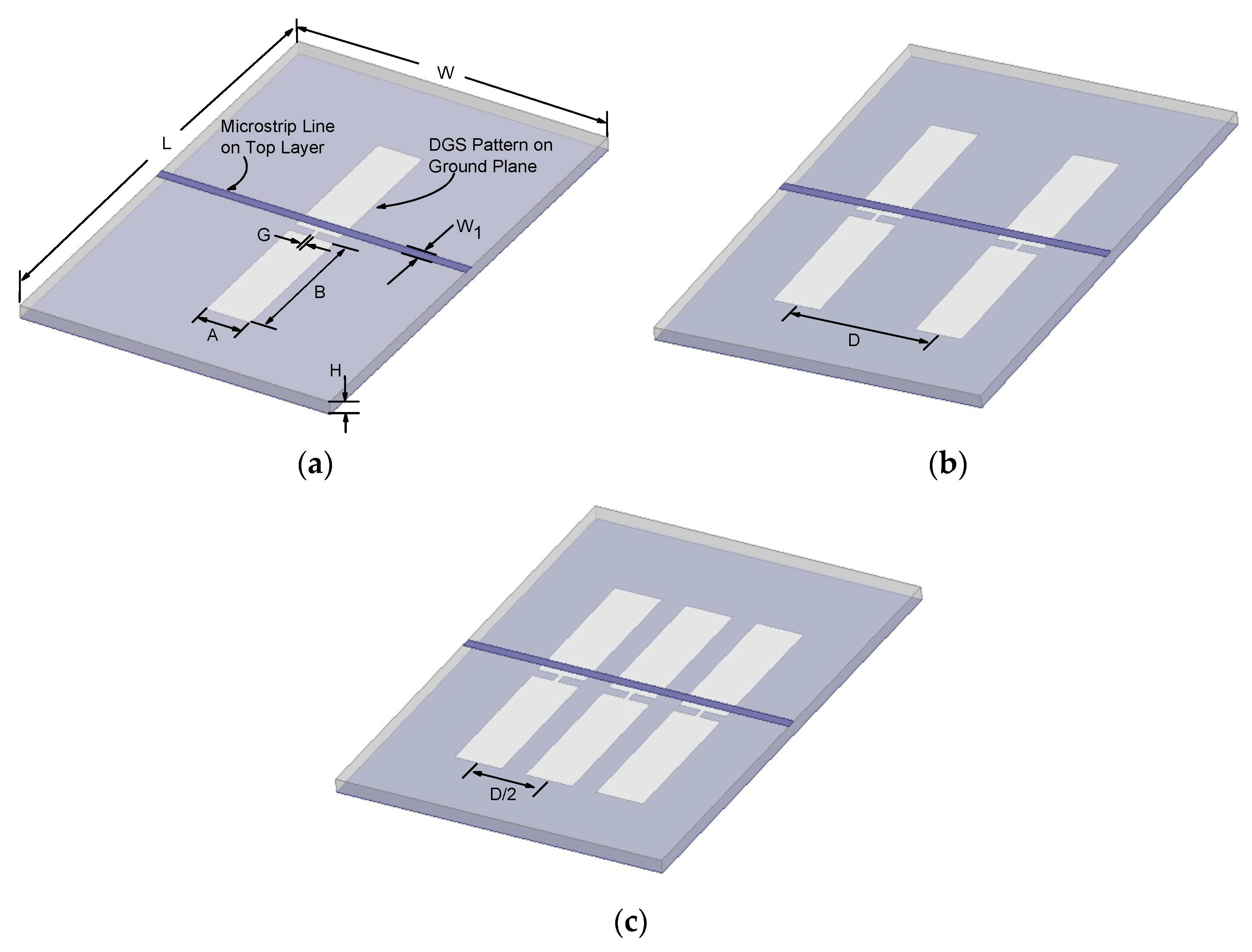
The DGS etched on the grounding metal plate for the microstrip circuit can be square-headed, semi-circular-headed dumbbell-shaped, and snake-shaped patterns. In this paper, the square-headed dumbbell-shaped DGS is applied. The 3-D model of one-, two- and three-DGS structures are shown in
Figure 1a–c.
The model of one-DGS structure in
Figure 1a is simulated in Ansoft HFSS. This model is designed on PTPE composite medium copper-clad foil plate with a relative dielectric constant
= 10.8 and a loss tangent of 0.0035. The distance of the middle slots is represented by
, the linewidth of microstrip line by
for 50-
characteristic impedance, and the width of DGS by
. The size of the whole model is about
. The detailed numerical values of the model are listed in
Table 1.
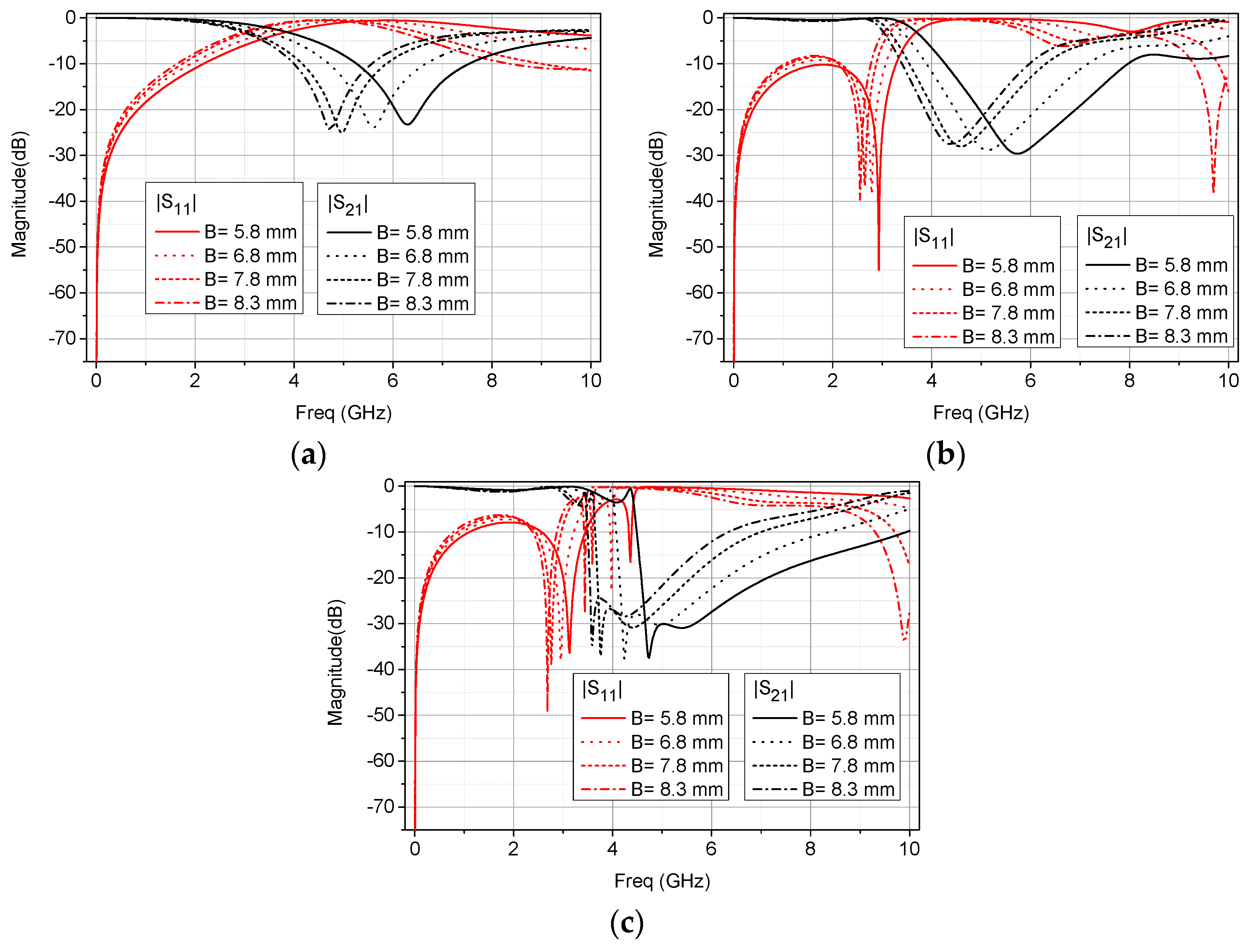
Figure 2a shows the simulated frequency responses of the return loss
and the insertion loss
of one-DGS case when the length
of DGS are 5.8, 6.8, 7.8, and 8.3 mm, respectively.
The transmission zero of the one-DGS structure shifts to the lower frequency band with the increasing length of
as shown in
Figure 2a. The frequencies of the transmission zero are 6.28 GHz, 5.62 GHz, 4.96 GHz, and 4.69 GHz, respectively. Further study shows that the frequencies of transmission zeros decrease with the increasing areas of DGS. Actually, the electrical property of the model of one DGS under the microstrip is equivalent to that of a parallel L-C resonator circuit. The growing area of the DGS corresponds to increasing the equivalent inductance of the parallel resonance circuit; the transmission zero therefore moves to the low frequency with increasing area of the DGS.
Similarly, the simulation frequency response characters of the models consisted of two- and three-DGS units which are presented in
Figure 1b,c and
Figure 2b,c, respectively. The distance between adjacent DGSs for two- and three-DGS models are
/2 = 3 mm. The sizes of the other parts are set up identical to the one-DGS case.
The transmission zeros of two- and three-DGS structures also move to the low frequency band with the increasing length of
as shown in
Figure 2b,c. By comparing the
Figure 2a–c, the frequency positions of transmission zeros decrease with the increasing number of DGS, and the width of the transition band (TB) between PB and SB greatly reduced in the three-DGS case. The interpretation of this phenomenon can be illustrated in
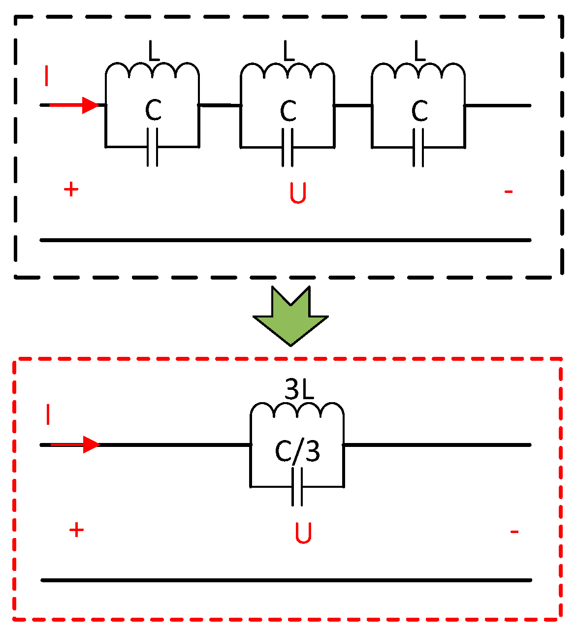
Figure 3.
The equivalent circuit model of the three-DGS model can be modeled by three parallel L-C resonators, as shown in the black dashed box in
Figure 3. The mutual coupling effects between each resonator are ignored because of a greater distance between the adjacent DGSs. The relations of the electric parameters for this circuit can be expressed as
Via simple mathematical transformation, Equation (1) converts into Equation (2)
The single equivalent parallel L-C resonator in the red dotted line in
Figure 3 reflects the relations of the electric parameters in Equation (2). Because the area of the DGS mainly affects the equivalent inductance of the parallel resonator, the three lengthening side lengths of B triple the parallel inductance. From DGS simulation in
Figure 2, it is known that the structure of DGS has the characteristics of low-pass filtering. Its low-pass characteristics can be adjusted by changing the defected area and shape etched on the grounding plate. This characteristic is applied to broaden the SB width of the SIR hairpin LPF in
Section 3.
3. Investigation of Proposed SIR Hairpin LPF
To realize the function of filtering, a filter requires one or more units of resonant structure. The resonant elements of SIR structure for filter designing is an effective way to realize compact filters. Lung-Hwa Hsieh et al. proposed a LPF using a SIR hairpin unit [
2]. On this basis, combined with M. Makimoto’s monograph [
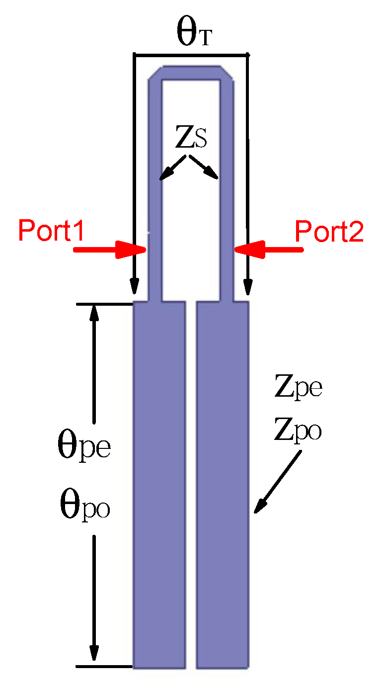
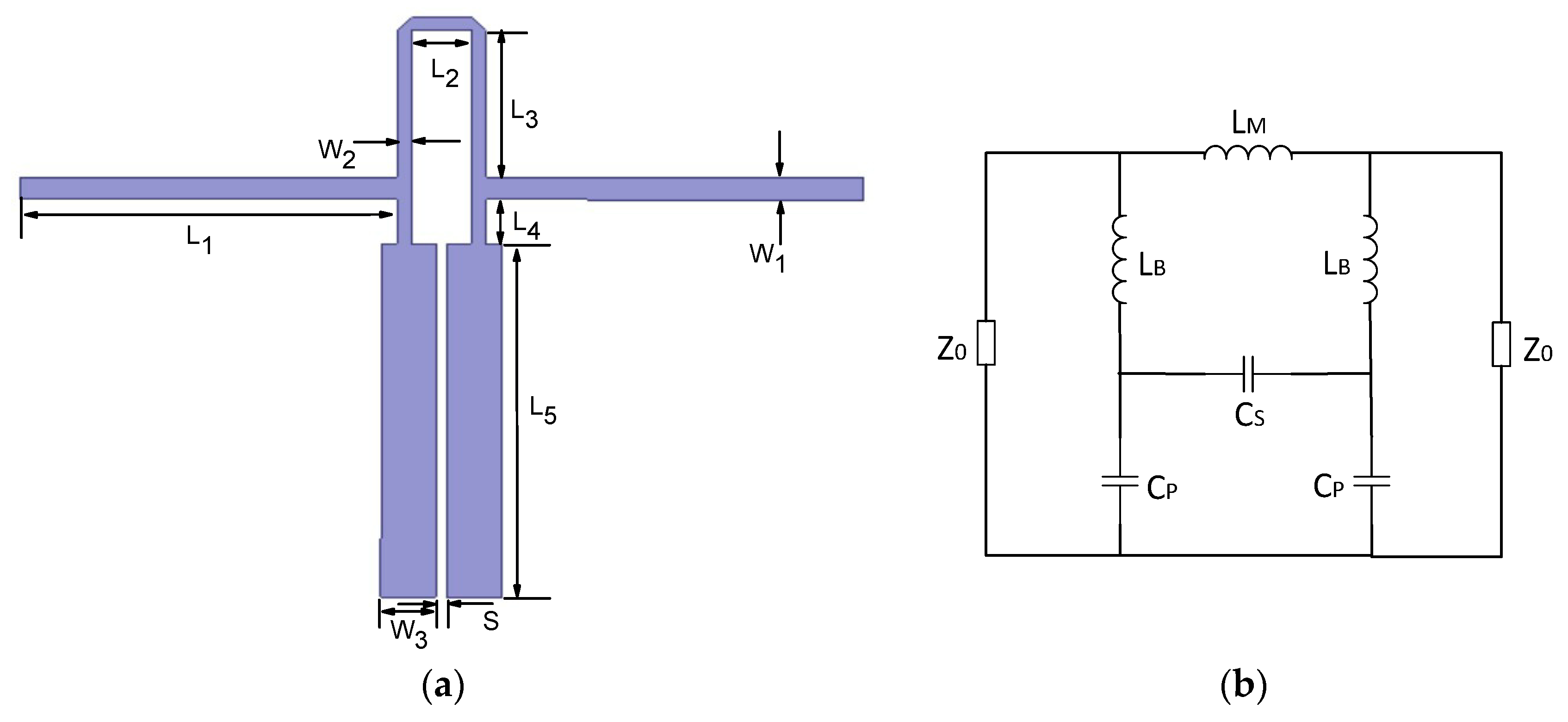
12], the following LPF with high attenuation edges are proposed. The cell structure is shown in
Figure 4.
The equivalent circuit of the resonator shown in
Figure 4 can be regarded as a parallel connection of a single transmission line and two parallel lines with internal coupling. The characteristic impedance and electric length of the single transmission line are
and
, respectively. The characteristic impedance (the electric length) of the even and odd modes of the parallel lines with internal coupling are
,
(
,
), respectively. The
matrix of the single transmission line and the parallel coupling line are expressed as
and
, respectively.
The matrix
is defined as the total
matrix of the above two parallel circuits.
where
where
=
due to
=
and
=
. A load impedance
is connected to the terminal in the circuit. The input admittance
can be calculated based on Equation (5):
The resonance condition is met under
= 0 and
=
, therefore, substituting the calculated value in Equation (5), the resonance condition is obtained as follows:
Based on the resonance condition of Equation (8), the characteristics of the above resonator can be analyzed using the microwave simulator method [
12].
Figure 5 shows the geometry of the resonator connected with two tapped microstrip lines and its equivalent circuit diagram.
The nonideal inductance
in
Figure 5b is the equivalent inductance of
,
,
and two
bends in
Figure 5a.
is the equivalent inductance of
. The non-ideal capacitances
,
are equivalent to the capacitances generated by two open coupling lines, in which
is generated by the coupling effect of two lines;
is generated by the coupling between the terminal microstrip line and the ground plate; and
is the characteristic impedance of two feeding lines. The equivalent circuit in
Figure 5b shows that the proposed structure has the property of an elliptic function-like LPF. The corresponding circuit model in
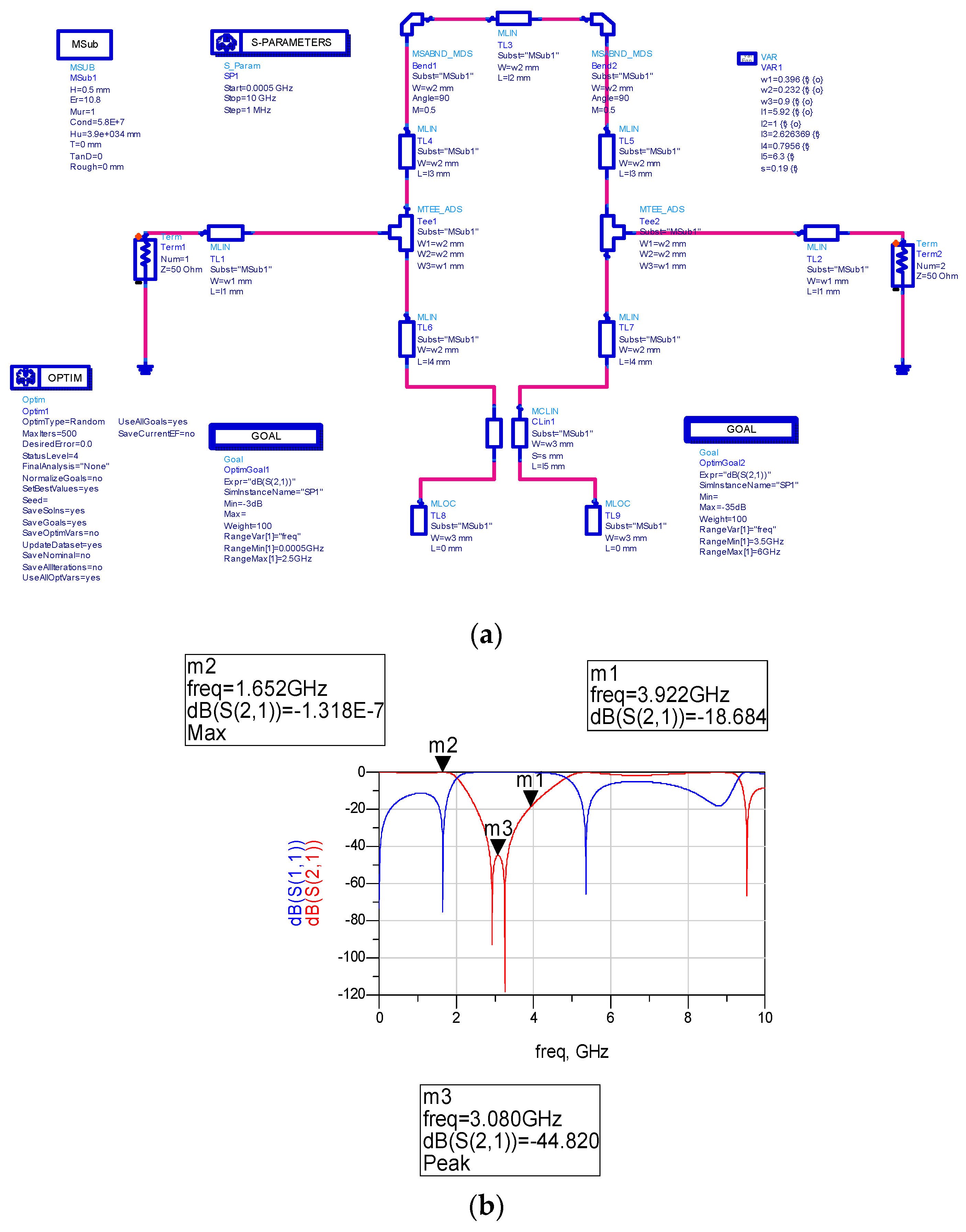
Figure 5a is simulated by ADS software. The simulation is to design a LPF with a cut-off frequency of 2 GHz under the condition that the relative dielectric constant of the microstrip substrate is 10.8 and the thickness of the substrate is 0.5 mm. The simulated schematic in ADS software is shown in
Figure 6a. To improve the frequency selectivity, the structural dimensions of the hairpin in
Figure 5a are obtained through software optimizing measures, which are listed in
Table 1. The transmission characteristics of the filters tuned by software are shown in
Figure 6b.
As shown in
Figure 6b, the proposed single SIR filter possesses the characteristic of high selectivity and produces two attenuation poles within a finite frequency band. This is the transmission characteristic of the three-branch elliptic function LPF. The disadvantage of this filter is that the SB width is narrow. Although the SB width can be properly enlarged by changing the size of each part of the SIR, it sacrifices the original characteristics of high frequency selectivity. Next, the SB width will be extended without changing the above structure sizes. That is to say, without changing the high edge frequency selectivity of the filter, the SB bandwidth is extended. The method is to introduce DGS structure.
4. Model Simulation and Sample Measurement
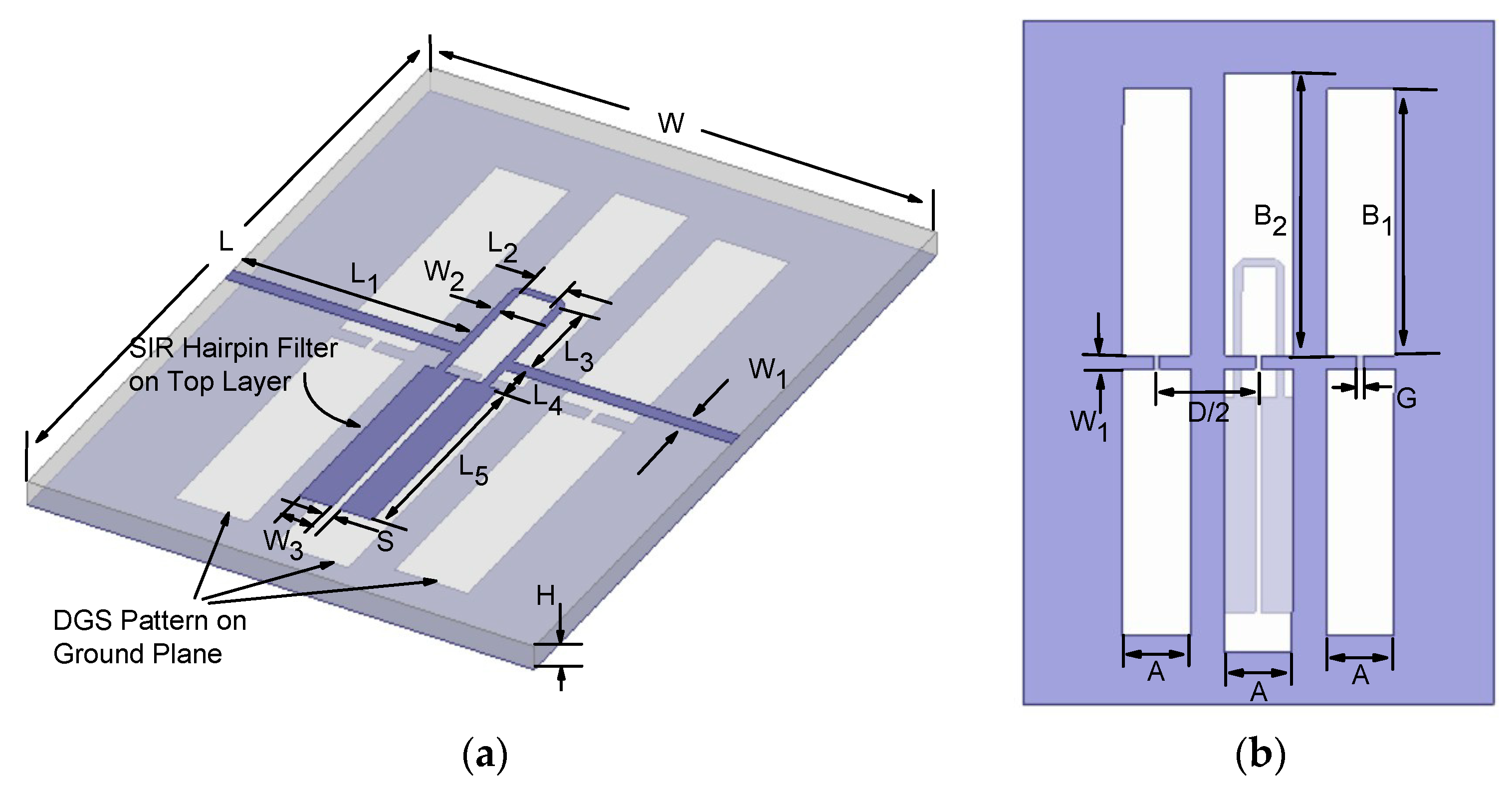
The proposed filter model is shown in
Figure 7 using the design method of combining DGS with an SIR hairpin filter. The optimized dimensions of the SIR hairpin filter on the top layer are identical to those in
Figure 5a. The sizes of the dielectric substrate and the three DGS patterns are the same with those in
Figure 1c except that the length of the middle GDS
is slightly longer than those of the two side GDS
. The optimized lengths of
and
are different in order to widen the valid SB width. The electrical parameters of the dielectric substrate and the size of each part of the filter are listed in
Table 1.
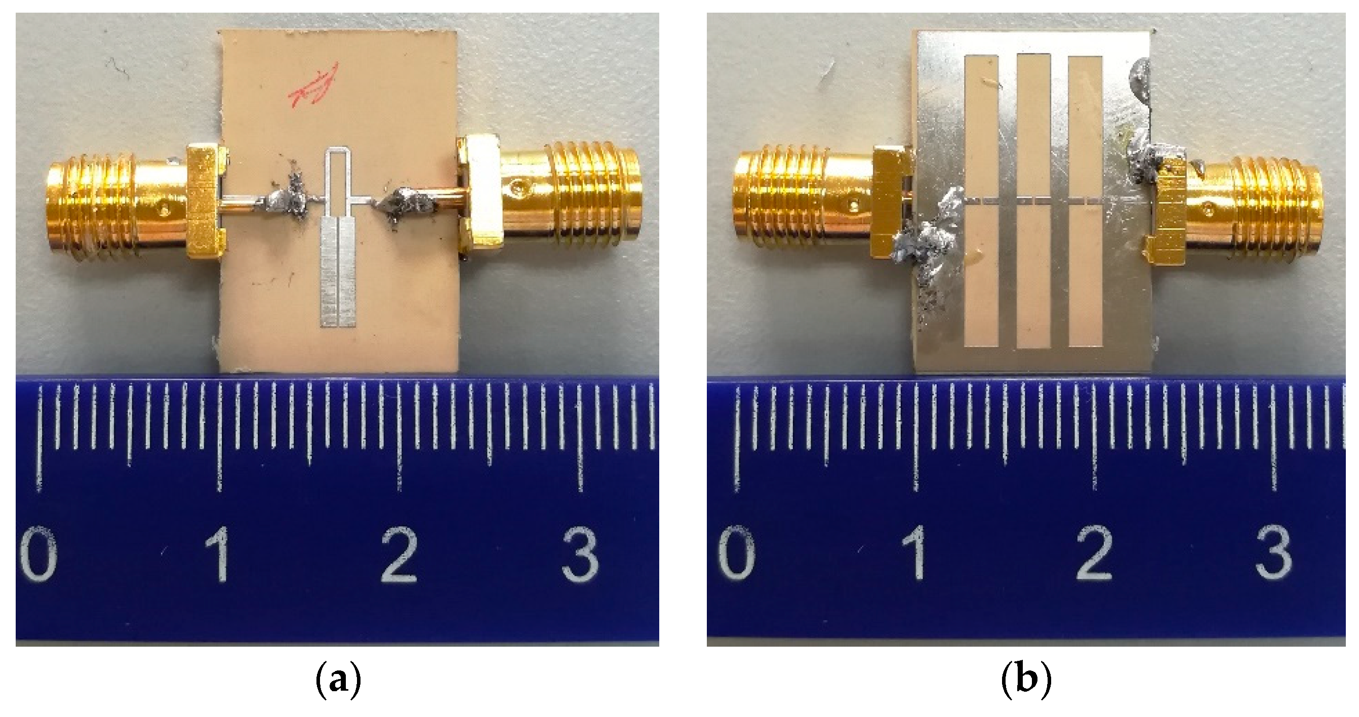
The proposed filter is fabricated and shown in
Figure 8. The Keysight N5224A PNA network analyzer is used to measure the S-parameters of the proposed LPFs.
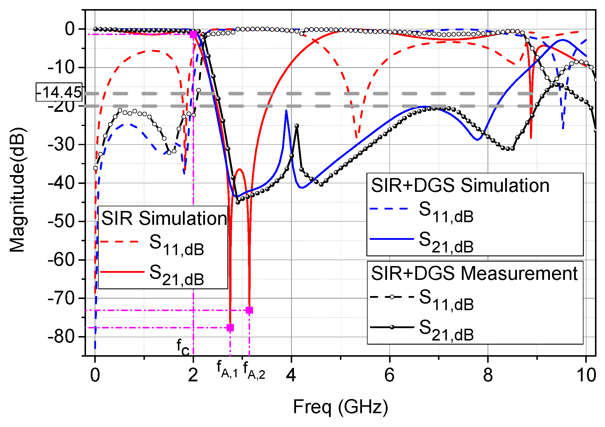
Figure 9 presents the simulated and measured results. The red lines are the S-parameters for a single SIR hairpin filter. These results obtained by full-wave electromagnetic simulation coincide with the results achieved by the circuit simulation using ADS software in
Figure 6.
From the simulation results in
Figure 9, it can be seen that the transmission coefficient of
is less than 0.38 dB from 0 Hz to 2 GHz, and the SB width is from 2.42 GHz to 8.2 GHz (see the blue curve) with a rejection of greater than 20 dB. Fortunately, the testing results show a broader SB width from 2.42 GHz to 9 GHz (see the black curve) with the same frequency selectivity and the attenuation in SB. The upper SB value even exceeds 10 GHz if the maximum attenuation degree is determined as 14.45 dB. The simulation and testing results are in good agreement.
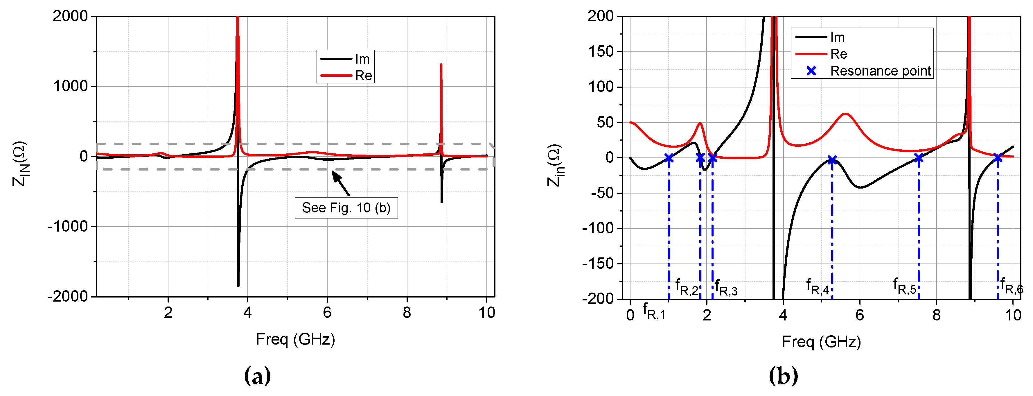
For the hairpin resonant filter, the simulated S-parameters shown in
Figure 9 by the red curves can be used to obtain the input impedance
[
1]:
where
=
/
is the load reflection coefficient, and
and
are the characteristic impedance of the transfer line and the load impedance, respectively. The
and
in our manuscript are also set to 50
. Therefore, the
= 50
/
and its values are shown in
Figure 10. From the
in
Figure 10b, it can be found that the first resonant frequency
= 1 GHz. Therefore, the SIR hairpin filter is a resonant element.
The quality-factor (Q) of a filter is the parameter to present the ratio of reactive power to active power. In the bandpass filter, the higher Q values mean the narrower bandwidth of the filter [
13]. Based on
, the quality-factor (Q) value is given by
=
/
. The Q values reach 1120, 1214 and 0.86 at the two attenuation poles
= 2.75 GHz,
= 3.14 GHz and the cut-off frequency
= 2 GHz, respectively. The Q values theoretically would be 0 at the resonant frequency points. The Q values at resonant frequency points
,
,
are very small values rather than zero, e.g.,
= 0.0078 at
. This is because the very accurate frequency points for resonance failed to take using the discrete digital computing method.
According to the S-parameters calculated in
Figure 9, we present the insertion loss (IL) in decibel form based on the equation of
=
=
[
1,
14,
15]. Therefore, the values of
are twice the values of
over the range of the investigated frequency.
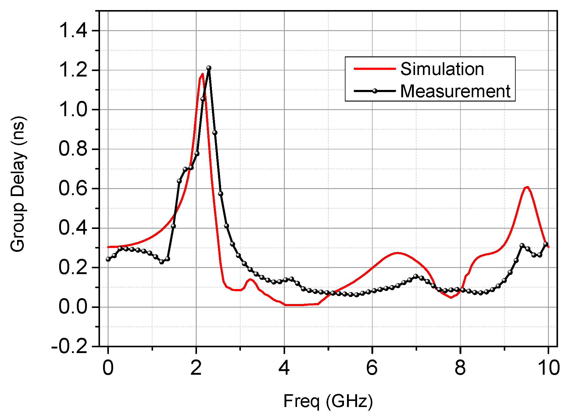
The group delay as the derivative of the phase varies as an important parameter in microwave filter design. The smaller the group delay variation, the better the flat property of the designed filter. The simulation and measured values of group delay are shown in
Figure 11. From this figure, the group delay varies from 0.23 to 0.78 ns in the pass band of 0~2 GHz. That is to say, the maximum variation of group delay is about 0.55 ns, representing a good flat property of the designed filter.
Some LPFs proposed in the references are compared with this paper in
Table 2. The proposed LPF in this paper has smaller pass-band ripple (PBR) by comparing with the LPF in Reference [
10]. The size of our designed LPF is less than those in Reference [
9,
11] with similar SB and TB width. The attenuation in stop-band (ASB) of LPF in Reference [
2] is better than that of our design, however, the size of the designed filter in the reference is larger than our proposed filter in this paper. Therefore, the LPF proposed in this paper possesses the properties of miniaturization, wide SB, high selectivity, and low PBR simultaneously.
5. Conclusions
Firstly, the square-headed dumbbell-shaped DGS is introduced. The transmission characteristics of one-, two- and three-DGS units are analyzed and compared by the 3D numerical simulation software HFSS. The results show that the structure of DGS has the property of low-pass filtering, and the SB attenuation extremum frequency decreases with the increase of the area and number of DGS units.
Secondly, a compact LPF is designed by using SIR hairpin resonator with internal coupling, which is equivalent to three-branch elliptic function LPF. The optimal sizes of the SIR LPF are obtained by the engineering electromagnetic software ADS of Agilent company. From the result of the simulation, this compact hairpin LPF has high frequency selectivity and very low PB attenuation, but the SB width under 20dB is not wide enough.
Finally, to extend the SB rejection width, we combine the DGS with the SIR LPF. By adjusting the area and number of DGS units, a microstrip LPF with small size, high frequency selectivity and wide SB suppression is achieved. Meanwhile, the maximum group delay variation in the passband is within 0.55 ns. The manufactured compact filter keeps good consistency with the simulation results, which proves the validity of the theoretical design. This compact LPF with excellent transmission performance is very suitable for the application of modern wireless communication circuits.
