Article

Analytical Design Solution for Optimal Matching of Hybrid Continuous Mode Power Amplifiers Suitable for a High-Efficiency Envelope Tracking Operation

1
Institute of Electronic Engineering, China Academy of Engineering Physics, Mianyang 621900, China
2
Department of Electronic Engineering, Tsinghua University, Beijing 100084, China
*
Author to whom correspondence should be addressed.
Electronics 2019, 8(6), 621; https://doi.org/10.3390/electronics8060621
Submission received: 27 April 2019 / Revised: 26 May 2019 / Accepted: 29 May 2019 / Published: 1 June 2019
(This article belongs to the Special Issue 5G Front-End Transceivers)

Abstract

:
An analytical method to design a power amplifier (PA) with an optimized power added efficiency (PAE) trajectory for envelope tracking (ET) architecture is proposed. To obtain feasible matching solutions for high-efficiency performance of the PA in the dynamic supply operation, hybrid continuous modes (HCM) architecture is introduced. The design space for load impedances of the HCM PAs with nonlinear capacitance is deduced mathematically using the device’s embedding transfer network, without the necessity of using load-pull. The proposed design strategy is verified with the implementation of a GaN PA operating over the frequency range of 1.9 GHz to 2.2 GHz with PAE between 67.8% and 72.4% in the 6.7 dB back-off power region of the ET mode. The ET experimental system was set up to evaluate the application of the PA circuit. Measurement results show that the ET PA at 2.1 GHz reaches the efficiency of 61%, 54%, 44% and an error vector magnitude (EVM) of 0.32%, 0.60%, 0.67% at an average output power of 34.4 dBm, 34.2 dBm, 34.1 dBm for 6.7 dB peak-to-average power ratios (PAPR) signals with 5 MHz, 10 MHz, and 20 MHz bandwidths, respectively. Additionally, tested by a 20 MHz bandwidth 16 quadrature amplitude modulation (QAM) signal, 41.8% to 49.2% efficiency of ET PA is achieved at an average output power of 33.5 dBm to 35.1 dBm from 1.9 GHz to 2.2 GHz.

1. Introduction

The current wireless communication schemes employ spectrally efficient complex modulation techniques to address the high data throughput demand. The dynamic wideband envelope and high peak-to-average power ratios (PAPRs) of 4G/5G waveforms challenge the RF power amplifier (PA) linearity–efficiency trade-off. Therefore, several architectures to improve the efficiency of RF PA have been investigated, e.g., Doherty, linear amplification with nonlinear components (LINC), envelope elimination and restoration (EER), and envelope tracking (ET) [1,2,3,4]. Unfortunately, architectures such as Doherty and LINC have bandwidth restrictions inherently. As for EER, the linearity of the signal is strongly dependent on the supply modulator and dependent on time-alignment between the RF phase signal and the amplitude envelope signal at the output of the PA [5]. However, these issues can be alleviated in envelope tracking (ET) architecture, which utilizes an envelope amplifier (EA) to instantly adjust the PA power supply voltage in synchronism with the envelope of the RF signal to ensure PA is always working at peak efficiencies for different output power levels. Since the EA is independent of the carrier frequency, the ET architecture has demonstrated considerable flexibility in multimode and multiband (MMMB) application scenarios. Moreover, the amplitude information is contained in the RF input under ET mode, and consequently, the envelope supply waveform can be de-troughed to prevent gain collapse and reduce the bandwidth of the envelope waveform [6], which is an advantage over EER.
The overall efficiency of the ET architecture is given by the product of the PA efficiency and EA efficiency. The state-of-the-art wideband EA circuits in the literature demonstrate average efficiency of 70% to 85%, depending on the signal bandwidth and the load impedance [7,8,9,10,11]. Therefore, to achieve more than 50% overall efficiency by considering the statistical probability distribution function (PDF) of the modulated signal, the power added efficiency (PAE) of the RF PA at the power back-off region should necessarily surpass 70%. This is a challenging task, since the change in drain-to-source capacitance ( C d s ) in the dynamic supply operation would result in a shift of the optimal load impedances to achieve high efficiency mode. Different modes, such as class-AB/B, class-J, and class-F Pas, have been investigated to overcome this limitation, whereas the art of ET’s RF PA design is still immature as the RF PA’s PAE at the power back-off region, i.e., the low drain supply voltage condition (corresponding to the average drain voltage of ET mode), is seldom above 70% at S-band [12,13,14,15].
This paper investigates, for the first time, the feasibility of utilizing hybrid continuous modes (HCM) PAs, which combine all the continuous modes between continuous Class-B/J and continuous Class-F [16], to optimize PAE trajectory for ET architecture. The design space for load impedances of the HCM PAs with nonlinear C d s is deduced mathematically using the embedding transfer network. Using the optimal impedance solutions at the package plane, a GaN high electron mobility transistor (HEMT)-based PA is designed and the simulated fundamental impedances in load–pull are in good conformity with the predicted ones based on the proposed method. The ET experimental system was set up to evaluate the application of the PA circuit. Measurement results show that the proposed ET PA exhibits competitive overall efficiency and linearity.

2. Feasible Design Space for ET Operation

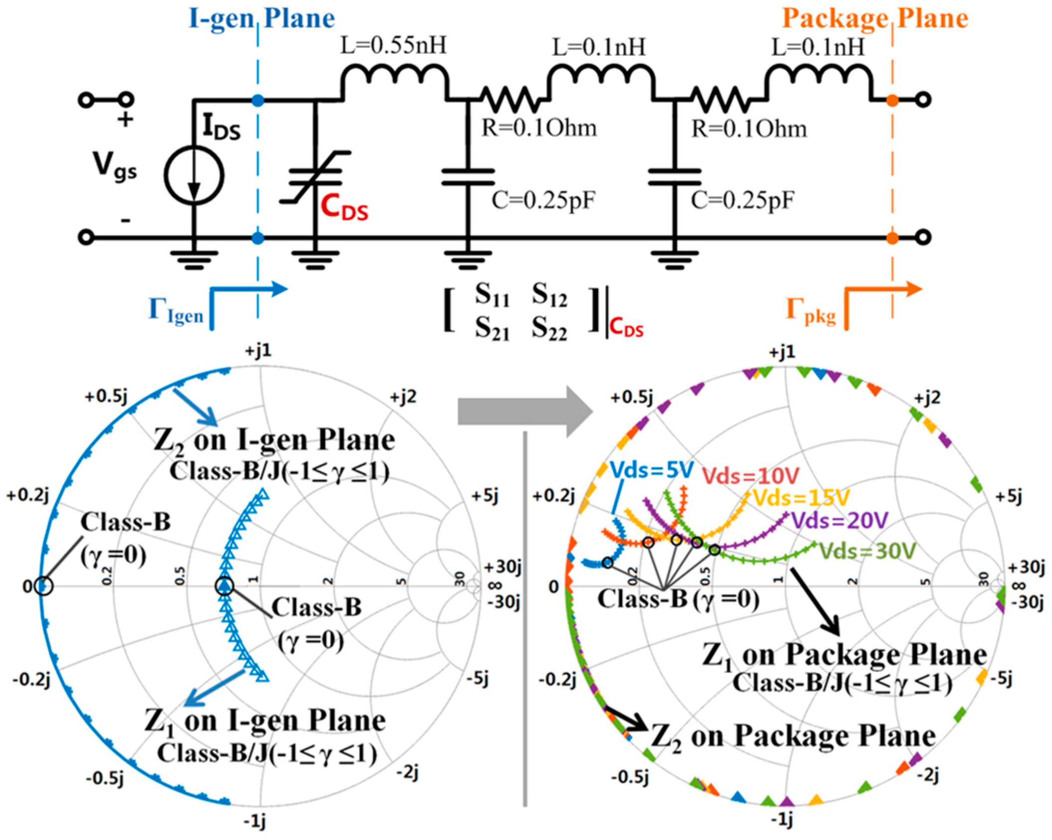
2.1. Nonlinear Capacitance and Parasitic Model

The variation of C d s with the drain voltage ( v d s ) is the main reason why conventional PA cannot be fully optimized over the full range of DC drain supplies (e.g., 3.5–30 V) under ET operation. It is therefore necessary to obtain a nonlinear capacitance model and embedding transfer network. The nonlinear C d s profile given by Equation (1) and the parasitic model extracted in [17] are used in this work, as shown in Figure 1. This network offers an approximated large-signal model for the Cree commercial GaN HEMT device CGH40010F (Cree Inc., Durham, NC, USA).
  C d s ( v ds ) = 0.95 + 1192.4 × [ 1 + tanh ( 0.0594714 × v ds 2.94696 ) ]   [ pF ] .
For simplicity, it is feasible to use average drain voltage V d s to calculate C d s , and then S-parameters ( S ( P ) ) of the embedding transfer network at different supply voltage can be computed conveniently utilizing the ABCD parameter matrix, as shown in Equation (2). Subsequently, the optimal impedances Z I g e n at the current generation plane can transform to Z p k g at the package plane.
S ( P ) = [ S 11 ( P ) S 12 ( P ) S 21 ( P ) S 22 ( P ) ] = [ A + B / Z 0 C Z 0 D A + B / Z 0 + C Z 0 + D 2 ( A D B C ) A + B / Z 0 + C Z 0 + D 2 A + B / Z 0 + C Z 0 + D A + B / Z 0 C Z 0 + D A + B / Z 0 + C Z 0 + D ]
Under different drain supply conditions, the multiple fundamental and harmonic impedance solutions of continuous class-B/J PA at both the current generation plane and package plane are calculated and shown in Figure 1. Evidently, the trajectory of the required impedances varies with drain supply voltage, which means that it would be inappropriate to select a fixed Z I g e n at different supply voltages. Another observation is that there is a possibility of achieving a fixed Z p k g when Z I g e n at different supply voltages are appropriately selected, which is beneficial to design matching circuits for ET’s RF PA.

2.2. Dynamic Envelope Supply Voltage

The PAE of the PA should be optimized at the drain bias corresponding to the maximum PDF of the supply envelope signal to achieve the maximum average efficiency under ET operation. In this work, a set of 16 QAM signals with 6.7 dB PAPRs are used to generate the dynamic envelope supply voltage signals. To avoid gain collapse at low drain voltages for the PA, the envelope signals are de-troughed using an exponential function proposed in [18].
The waveform of the de-troughed envelope signal and correspondent envelope amplitude PDF is illustrated in Figure 2. The de-troughed envelope voltage varies from 3.5 V to 30 V, and there is the highest probability that envelope amplitude voltage is close to 15 V. Considering the value range of nonlinear C d s , it is appropriate that the drain bias of 15 V, 20 V, and 30 V are selected when the optimal impedance of the PA is targeted.

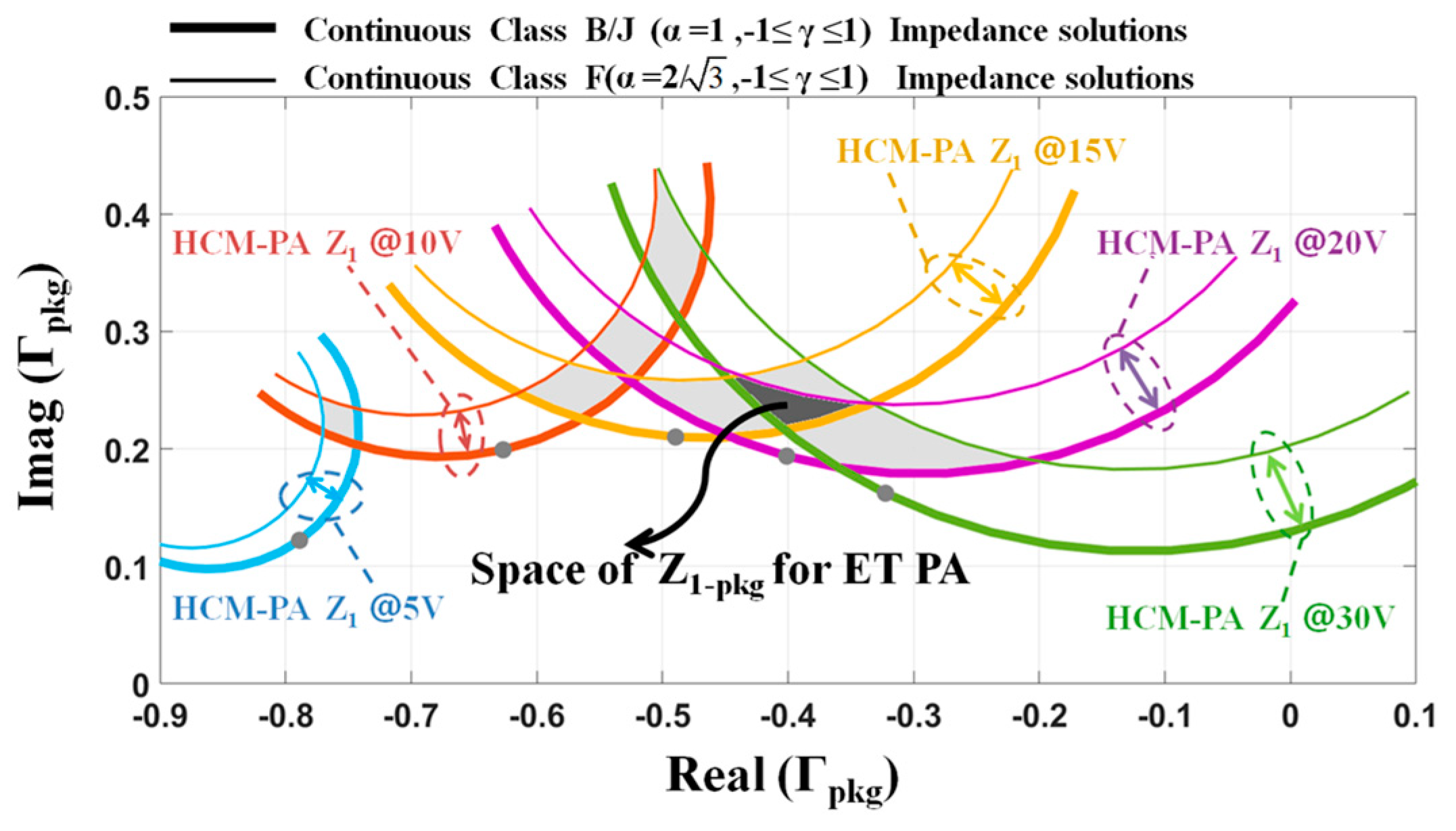
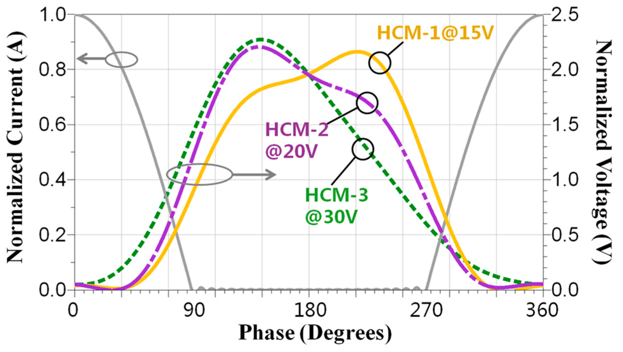
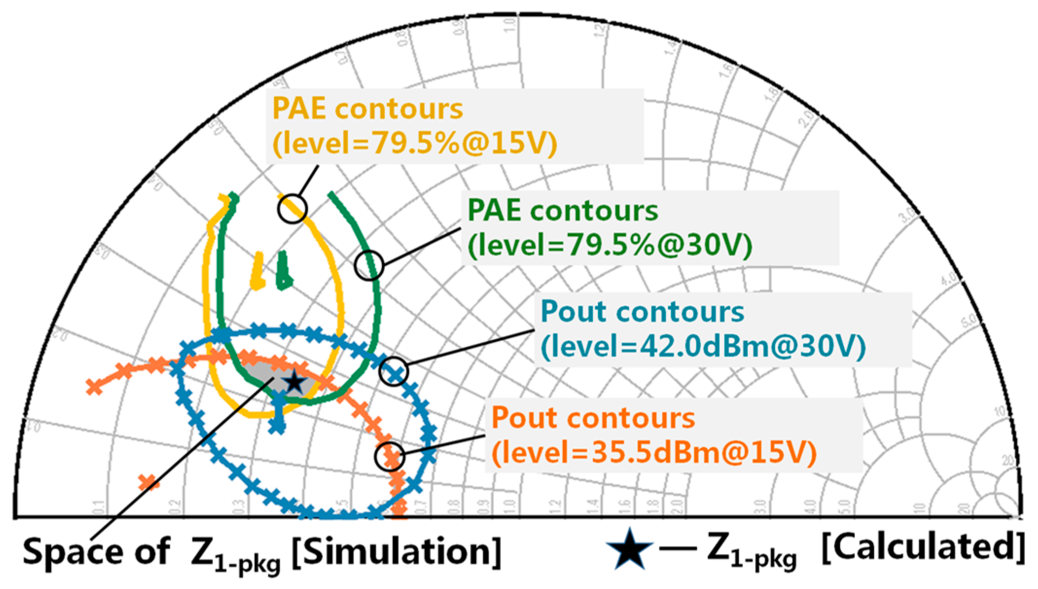
2.3. HCM PAs Design Space for PAE Trajectory Optimization

The HCM PAs illustrated in Equation (3) combine continuous Class-B/J ( α = 1 , β = 0 ) and continuous Class-F ( α = 2 / 3 , β = 1 / 3 3 ), and the different values of α and β correspond to different continuous modes [16].
v d s ( t ) = ( 1 α cos ( ω t ) + β cos ( 3 ω t ) ) × ( 1 γ sin ( ω t ) )               1 γ 1
It is shown in [19] that for obtaining high efficiency in the Class-J and Class-F case, the nonlinear device output capacitance can reduce the sensitivity to the second and third harmonic impedance terminations. So it is reasonable that the design of this work focuses more on the fundamental match.
HCM PAs obviously expand design space for realizing high-efficiency performance and can maintain the output power and efficiency above classical Class-B. Figure 3 shows the multiple fundamental impedance solutions of HCM PAs at the package plane. There exists a common area of impedance solutions when the drain supply voltage is above 15 V, which gives more design freedom for realizing ET PA. To explain the design methodology of this work in detail, a mathematical analysis process is presented as follows.
Drain supply voltages are set to 15 V, 20 V and 30 V, respectively, as mentioned above, then S ( P ) can be extracted from the embedding transfer network and be described as
S ( P i ) = [ S 11 ( P i ) S 12 ( P i ) S 21 ( P i ) S 22 ( P i ) ]               i [ 1 , 2 , 3 ] .
The fundamental impedance at the current generation plane with different supply voltages is represented by
Z 1 _ I g e n ( α i , γ i ) = R o p t ( α i + j γ i )               i [ 1 , 2 , 3 ] ,
where R o p t = 2 ( V D C V K n e e ) / I M a x , and R o p t = 36   Ω is chosen for CGH40010F in this work. Then reflectance at the current generation plane and package plane can be described as
Γ 1 _ I g e n ( α i , γ i ) = Z 1 _ I g e n ( α i , γ i ) Z 0 Z 1 _ I g e n ( α i , γ i ) + Z 0 ,
Γ 1 _ p k g ( P i ) = Γ 1 _ I g e n ( α i , γ i ) S 11 ( P i ) S 21 ( P i ) S 12 ( P i ) S 11 ( P i ) S 22 ( P i ) + S 22 ( P i ) Γ 1 _ I g e n ( α i , γ i ) .
To evaluate the distance between impedance solutions at the package plane under different drain supply conditions, parameter L is defined as
L = | Γ 1 p k g ( P 1 ) Γ 1 p k g ( P 2 ) | + | Γ 1 p k g ( P 1 ) Γ 1 p k g ( P 3 ) | + | Γ 1 _ p k g ( P 2 ) Γ 1 _ p k g ( P 3 ) | .
The minimum of L can be found for different modes of PA. For HCM PAs the problem can be expressed as
m i n L ( α 1 , α 2 , α 3 , γ 1 , γ 2 , γ 3 ) s . t . 1 α 1 2 / 3 1 γ 1 1     i [ 1 , 2 , 3 ]
Table 1 summaries the calculated results of PA design parameters utilizing numeric analysis. Obviously, HCM PAs can provide design space for achieving a fixed Z 1 _ p k g to realize impedance matching optimization at different supply voltages. Theoretically, there is a large number of solutions for Equation (9), and the result in Table 1 is one suitable for practical realization. The normalized drain voltage and current waveforms of HCM PAs presented in Table 1 have little overlap, as shown in Figure 4, which indicates that the proposed solution has very low power dissipation over a wide range of drain supply.

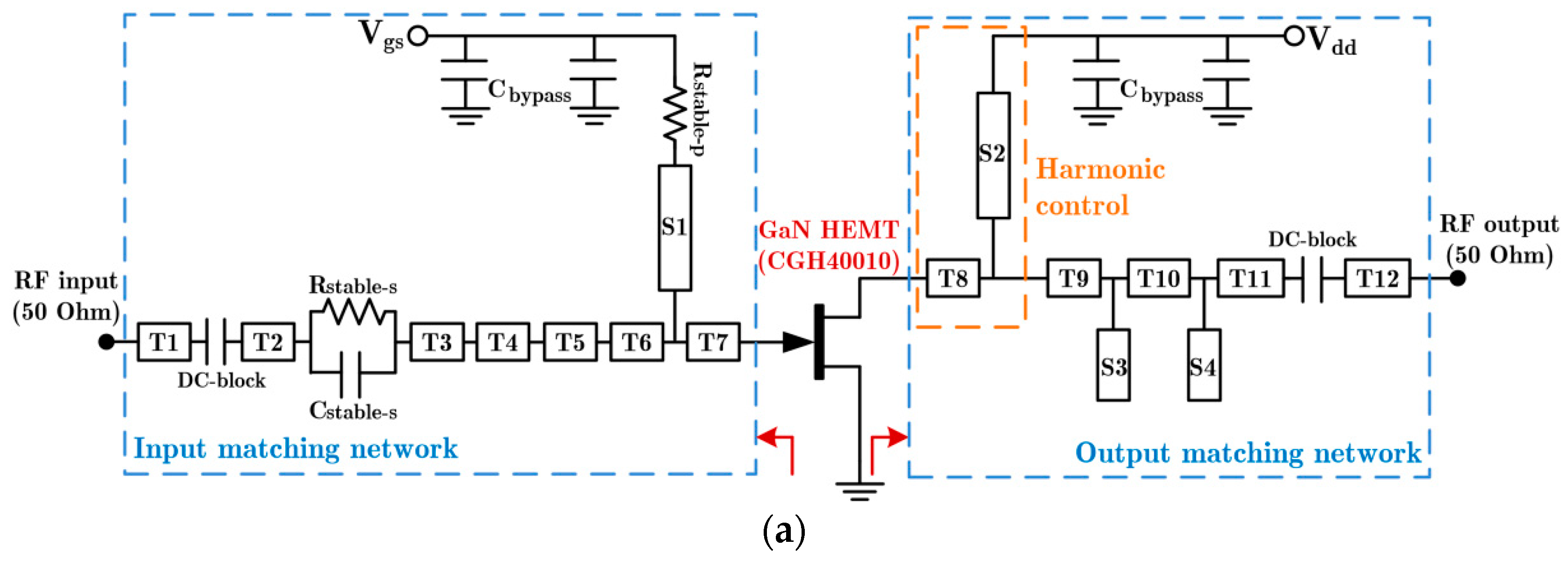
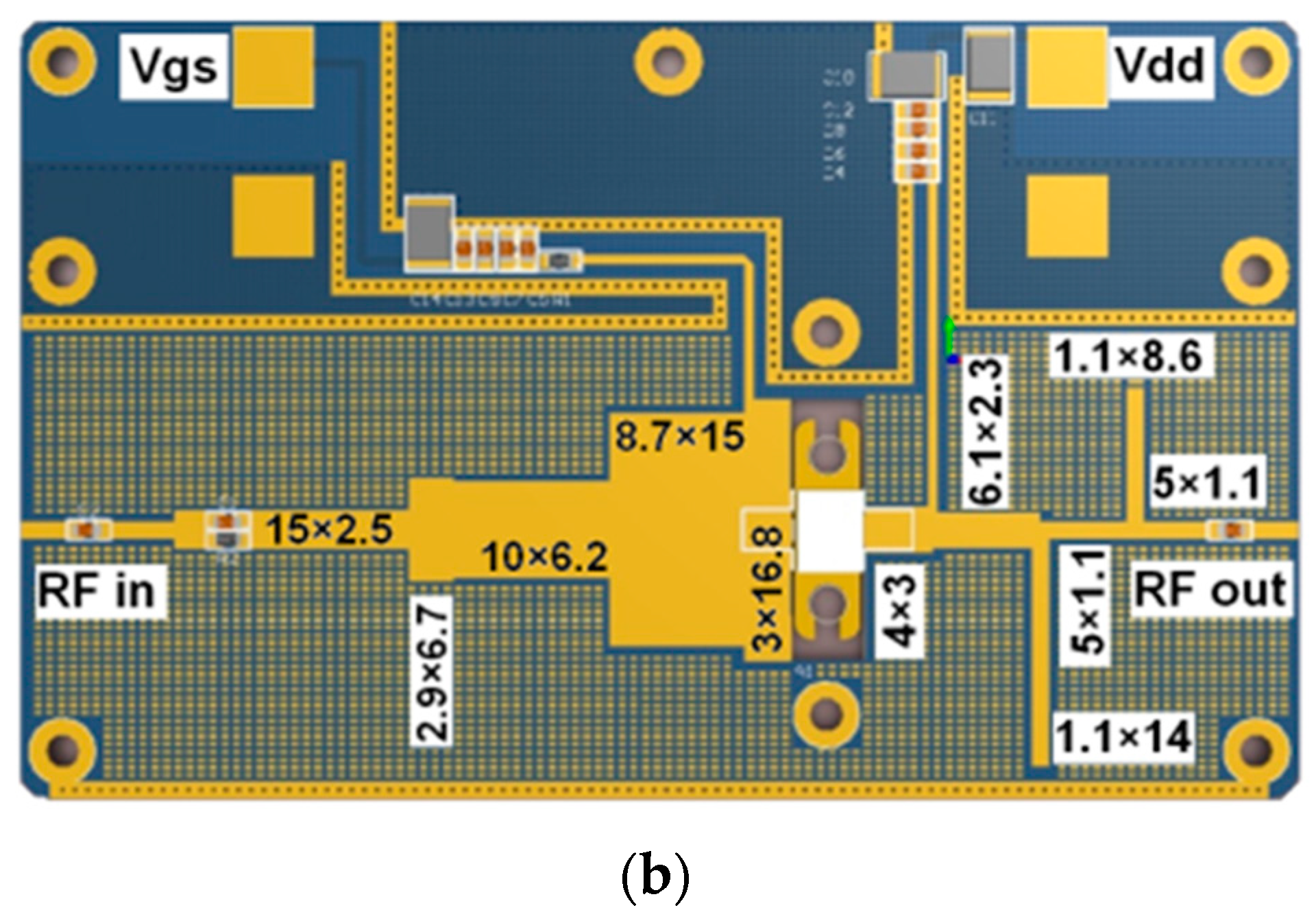
2.4. PA Implementation and Test

To verify optimum fundamental load impedance proposed above, the load–pull simulation was carried out, and the PA circuit was fabricated. In the simulation, the optimum fundamental load impedance is determined by analyzing output power and PAE contours at different drain supply. Figure 5 shows that there is a feasible solution space to provide high PAE (79.5%) and proper output power at both 15 V and 30 V drain bias, which is of benefit to ET operation.
The calculated Z 1 _ p k g in Section 2.3 is also presented in Figure 5, as a comparison with the simulated results, which proves the validity of the proposed design strategy in this work. Additionally, the harmonic load impedance in this work is chosen to the edge of the Smith chart with the constraints of high efficiency and high power regions, and optimum fundamental source impedance is picked out with resorting to source pull simulation.
The input and output matching network schematic of the proposed PA circuit is shown in Figure 6a. The input fundamental matching network, considering the stability by adding a serial resistor-capacitor and parallel resistor, is matched to optimum fundamental source impedance. For the purpose of designing a broadband matching network conveniently, conventional multiple sections of transmission line topology are used in the input matching circuit. In addition, the optimum load impedance Z 1 _ p k g at fundamental frequency can be matched by using the output matching network. To optimize efficiency and output power of the proposed PA, the second harmonic control circuit, which is constituted of the quarter wave transmission line S2 and matching transmission line T8, is adopted to restrict the second harmonic impedance roll-off to the edge of the Smith chart. The matching networks are implemented on substrate RO4350B from Rogers Inc. (Chandler, AZ, USA), with a dielectric constant of 3.66 and thickness of 0.508 mm. The matching network layout of the proposed PA circuit is illustrated in Figure 6b.
The measured gain and PAE at various supply voltages as a function of output power together with the statistical PDF of the modulated signal are shown in Figure 7. The blue dots on the gain and PAE curves represent the gain trajectory and PAE trajectory of the ET operation. The maximum drain supply is set to 27.5 V, and the corresponding output power is about 42 dBm. The minimum drain supply is set to 5 V, and the corresponding peak output power is about 24 dBm. Note that the peak PAE exceeds 70% when drain supply is set from 12.5 V to 27.5 V. That means the proposed PA provides high PAE over a wide range of output powers. This behavior ensures high overall efficiency for the ET architecture. The performances of the demonstrated PA are listed in Table 2, in comparison with the state-of-the-art ET PAs in the literature.

3. Envelope Tracking Transmitter Experimental System

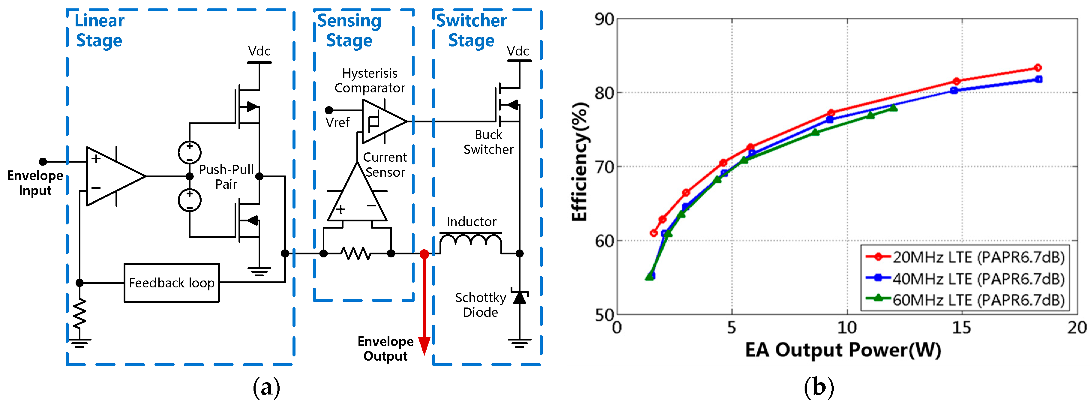
3.1. High Efficiency and Wideband Hybrid Envelope Amplifier

To evaluate the application of the PA circuit, the overall ET transmitter experimental system was set up for testing. Since the overall efficiency of the ET system is roughly the product of efficiencies of the EA circuit and the RF PA circuit, a high efficiency and wideband EA circuit is another key part of the ET transmitter. The designed EA circuit in this work has a hybrid structure, which is composed of a linear stage, a sensing stage, and a buck switcher stage [20,21], as shown in Figure 8a. The reason for using the hybrid architecture relies on the characteristics of the input envelope signal [22].
The designed EA is tested with a 7.5 Ω resistive load for efficiency and accuracy verification. A group of 6.7 dB PAPR 16 QAM signals with 20 MHz, 40 MHz, and 60 MHz modulation bandwidths are employed to generate the envelope signals. The efficiency of the EA modulator is measured and shown in Figure 8b. Using 40 MHz 6.7 dB PAPR signal, it achieves an efficiency of 82% at the average output power of 18.3 W and over 70% efficiency when the output power is larger than 5 W. In addition, the small signal 3 dB bandwidth of the EA circuit is 209 MHz, which implies that it can support wide bandwidth envelope inputs.

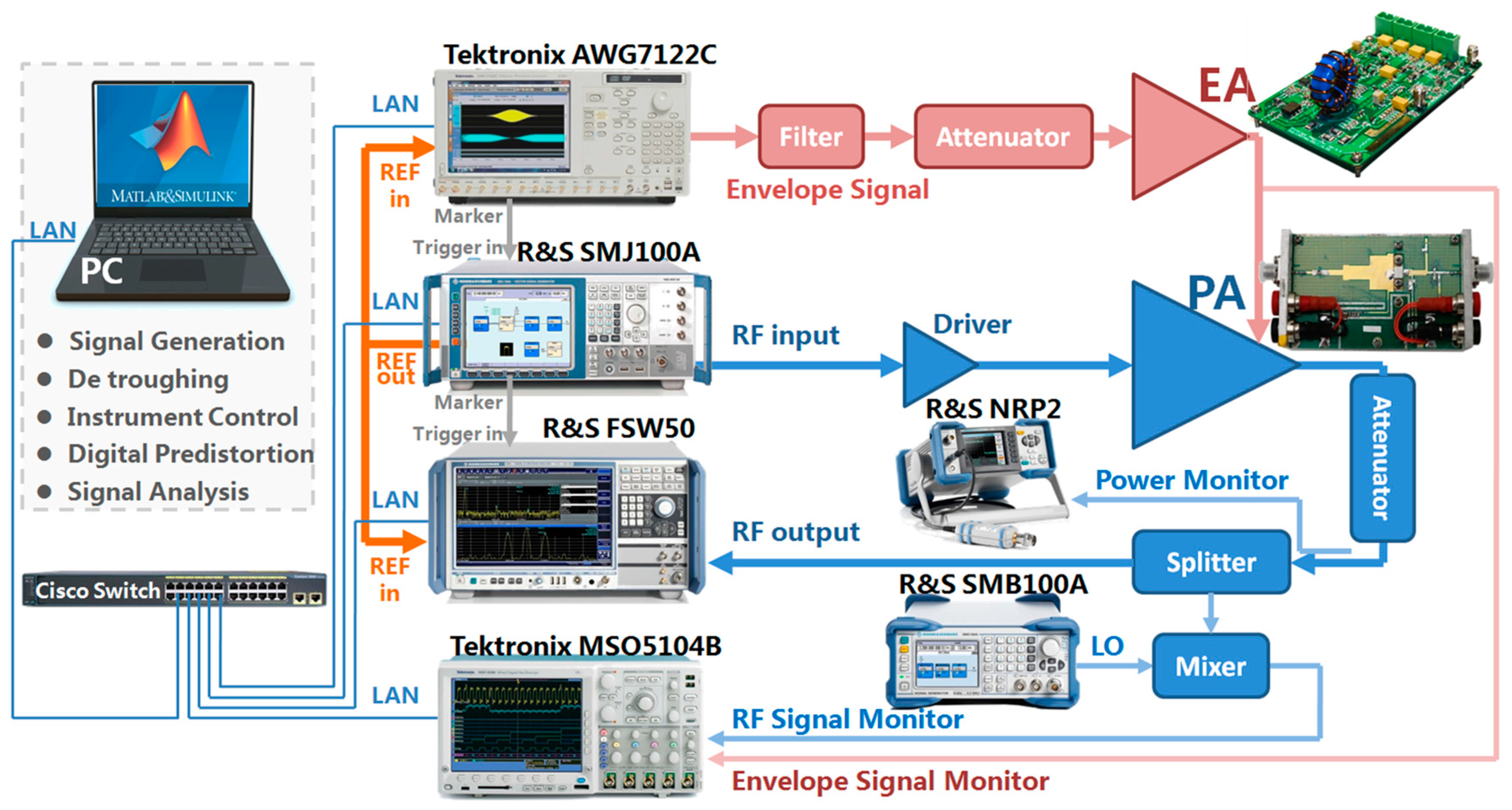
3.2. Measurement Setup

Figure 9 presents the ET experimental system diagram. The testing signals are 5 MHz, 10 MHz, and 20 MHz bandwidths 16 QAM long term evolution (LTE) signals with 6.7 dB PAPR at 2.1 GHz. The baseband modulated signals and envelope signals were generated and pre-processed in MATLAB in PC, and they were streamed to the R&S SMJ100A (R&S Inc., Munich, Bayern, Germany) and Tektronix AWG7122C (Tektronix Inc., Beaverton, OR, USA), respectively.
The ET system includes an RF signal path and an envelope path. In the RF path, the up-converted RF signals from VSG are amplified by the driver, and then the output of the driver is provided to the input of the PA. The PA output comes into the spectrum analyzer R&S FSW50 (R&S Inc., Munich, Bayern, Germany), which can capture and record the baseband data of the transmitter system. In the envelope path, the wideband and high-efficiency EA amplifies the generated envelop signals from the AWG, and modulates the drain supply of the PA. To minimize the distortion caused by the time misalignment between the envelope path and the RF path, synchronization needs to be performed. The EA output envelope and the down-converted RF signal are monitored by a high speed oscilloscope Tektronix MSO5104B (Tektronix Inc., Beaverton, OR, USA). In the digital signal processing, an envelope-enhanced memory polynomial DPD model [7] is extracted by using the time-aligned input and output data of the ET system. Finally, the pre-distorted input is downloaded again to rectify the nonlinearity of the ET transmitter.

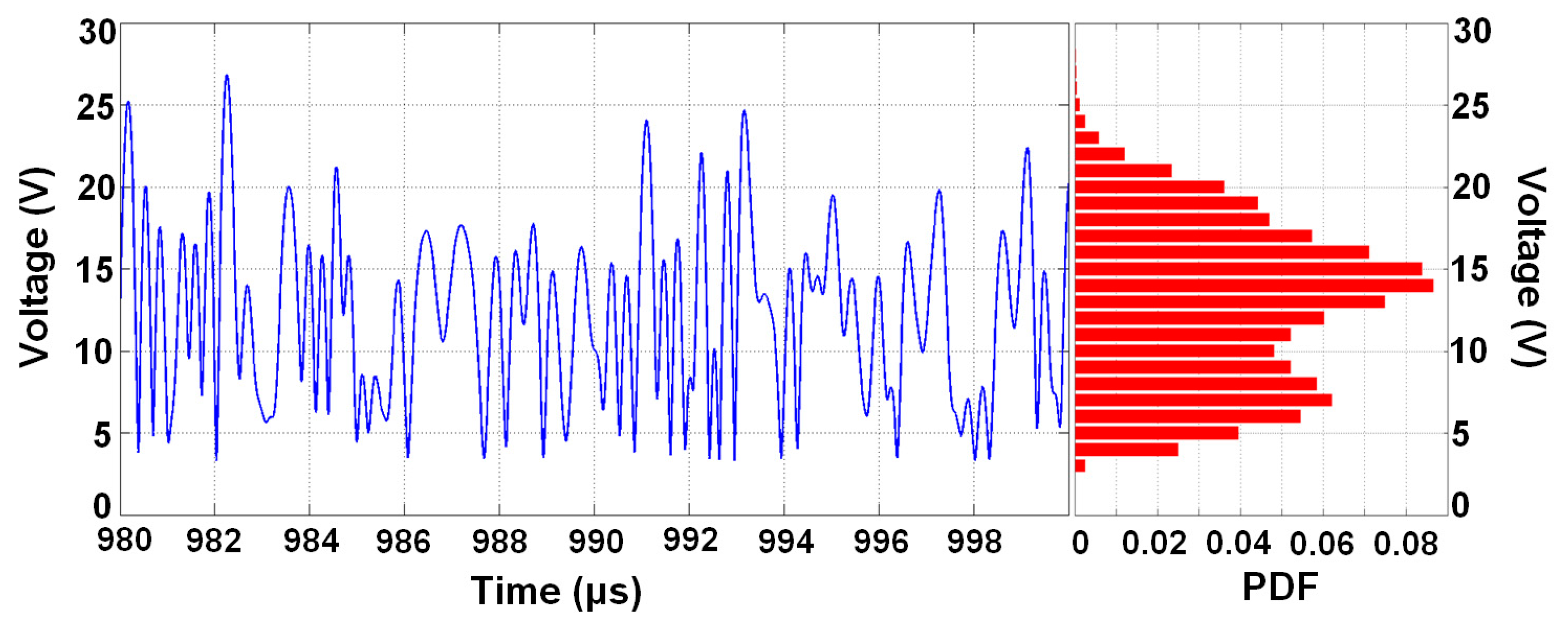
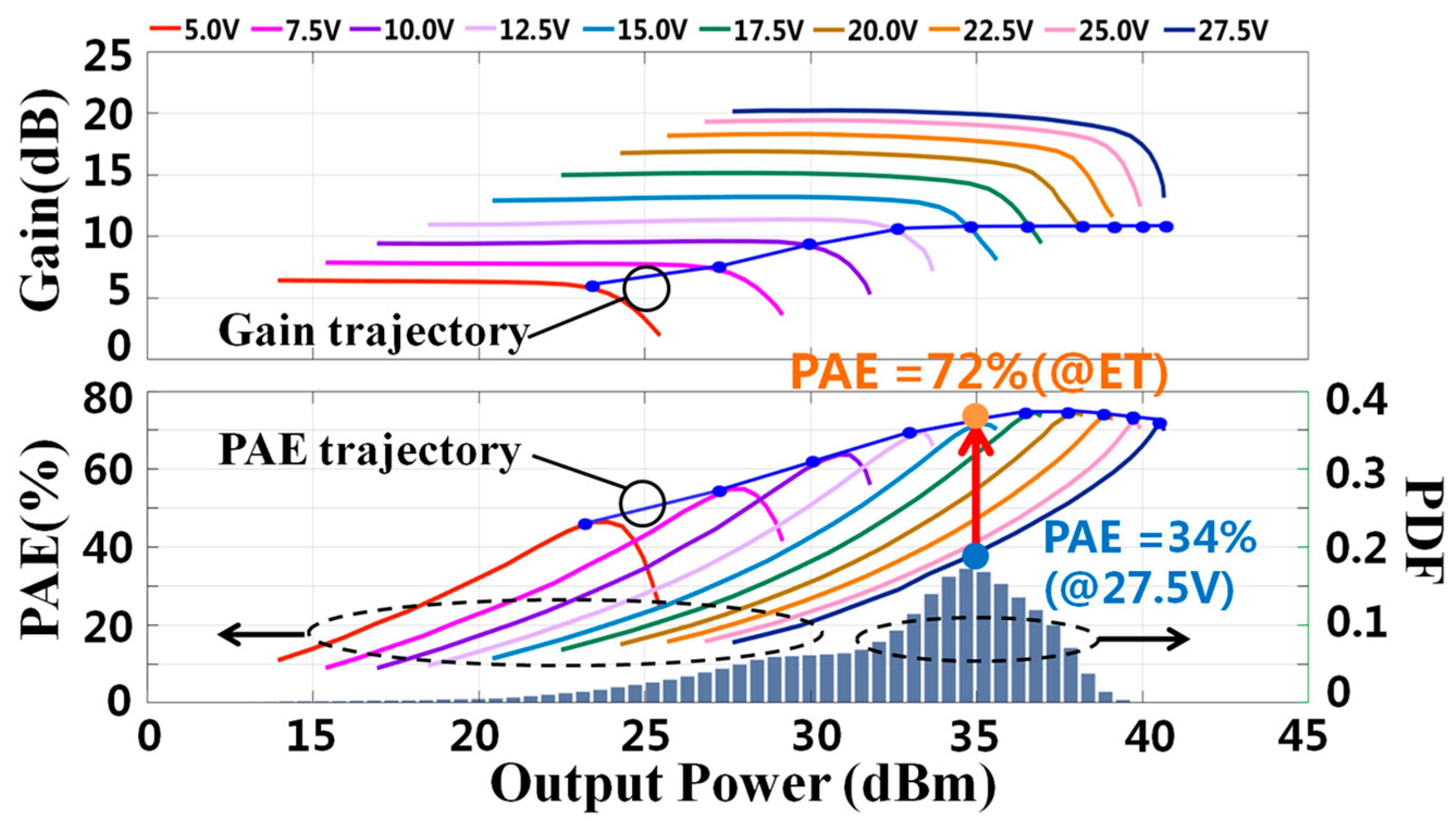
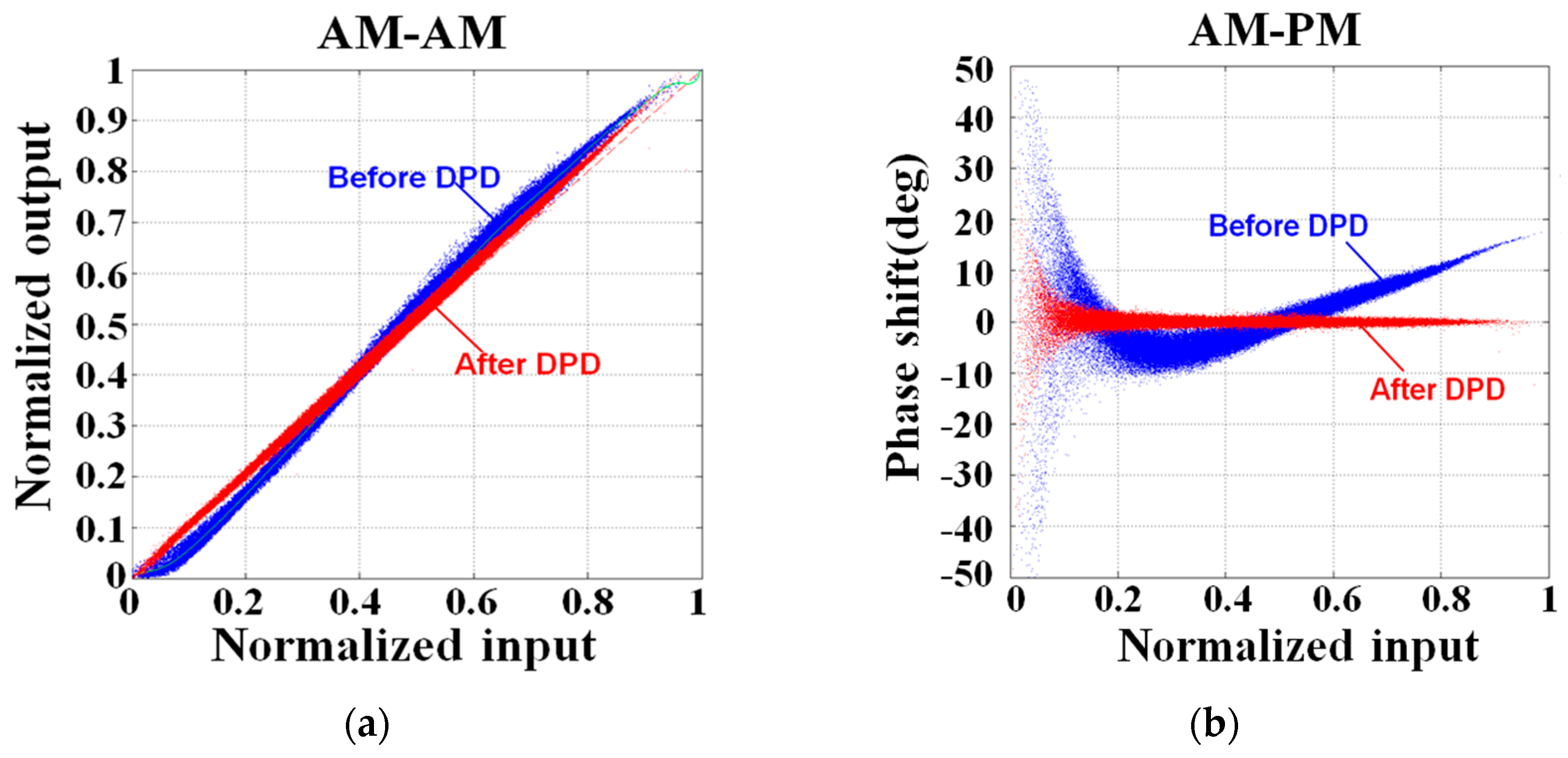
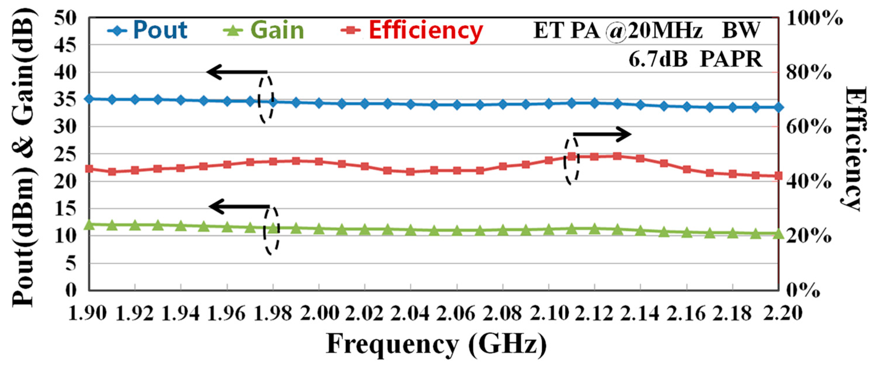
4. Measurement Results

Table 3 summaries the measurement results which demonstrate the ET system performance. The ET transmitter obtains the measured efficiency of 60.8%, 53.7%, 44.1% and error vector magnitude (EVM) of 0.32%, 0.60%, 0.67% at an average output power of 34.4 dBm, 34.2 dBm, 34.1 dBm for 6.7 dB PAPR 16 QAM LTE signals with 5 MHz, 10 MHz, and 20 MHz bandwidths, respectively. Figure 10 shows the representative measured waveforms (20 MHz bandwidth (BW) LTE at 2.1 GHz) for RF output, drain voltage, and switching state in the ET experimental system. The drain supply voltage closely tracks the RF PA output envelope, which indicates that the proposed PA is working at high-efficiency ET mode.
The digital pre-distortion (DPD) technique can compensate the nonlinear distortion well enough to ensure high signal quality of the transmitter. Measured ET transmitter output spectra (20 MHz BW LTE at 2.1 GHz) before and after DPD are presented in Figure 11. It is apparent that the output spectrum shows less spectral re-growth and a 20 dB reduction in adjacent channel power ratio (ACPR) can be achieved after using the DPD technique.
In addition, without DPD, ET PA shows significant AM-AM and AM-PM distortion with memory effects. Figure 12 shows the detailed AM-AM and AM-PM characteristics of the ET PA, before and after DPD. Obviously, the linearity of the ET PA in this work can be improved with the DPD technique.
ET PA can support multi-band operation since the EA circuit is independent of the carrier frequency. To show the broadband performances of ET PA, experiments were also performed at different frequencies. Tested by 20 MHz BW, 6.7 dB PAPR 16 QAM signal, 41.8% to 49.2% overall efficiency of ET PA is achieved at an average output power of 33.5 dBm to 35.1 dBm from 1.9 GHz to 2.2 GHz, as shown in Figure 13. Evidently, the proposed PA is quite suitable for a high-efficiency ET mode, and it has great potential for upgrading the broadband characteristics in a dynamic supply operation.

5. Conclusions

The feasibility of utilizing HCM PAs to optimize PAE trajectory for ET architecture is investigated for the first time. The design space for load impedances of the HCM PAs with nonlinear capacitance is deduced mathematically using the device’s embedding transfer network. The proposed design methodology has been verified by extensive experiments. Measurement results show that ET architecture with the proposed PA circuit exhibits competitive overall efficiency and linearity for high PAPR modulation signals in a wide RF frequency range.

Author Contributions

T.C. conceived the methodology, performed the experiments, and wrote the initial draft. Y.L. and W.C. provided significant comments and technical feedback throughout the research. C.Y. reviewed and revised the final draft. J.Z. financially supported this work.

Funding

This research was funded by the National Natural Science Foundation of China, grant number 61601425, and the Presidential Foundation of China Academy of Engineering Physics, grant number YZJJLX2017006.

Acknowledgments

The authors would like to thank the Keylink Microwave Technology Company Limited of China for providing technical support in circuits fabrication.

Conflicts of Interest

The authors declare no conflict of interest.

References

  1. McKnight, K.; Darwish, A.; Zaghloul, M. A Compact Output Power Combiner for Broadband Doherty Power Amplifiers. Electronics 2019, 8, 275. [Google Scholar] [CrossRef]
  2. Ramella, C.; Piacibello, A.; Quaglia, R.; Camarchia, V.; Pirola, M. High Efficiency Power Amplifiers for Modern Mobile Communications: The Load-Modulation Approach. Electronics 2017, 6, 96. [Google Scholar] [CrossRef]
  3. Tena-Ramos, D.; Patino-Gomez, M.; Ortega-Gonzalez, F.J. Hybrid Envelope Elimination and Restoration Technique for Enhancing the Linearity of Switchmode Envelope Amplifiers. IEEE Microw. Wirel. Components Lett. 2017, 27, 186–188. [Google Scholar] [CrossRef]
  4. Asbeck, P.; Popovic, Z. ET Comes of Age: Envelope Tracking for Higher-Efficiency Power Amplifiers. IEEE Microw. Mag. 2016, 17, 16–25. [Google Scholar] [CrossRef]
  5. Jeong, J.; Chaudhary, G.; Jeong, Y. Time Mismatch Effect in Linearity of Hybrid Envelope Tracking Power Amplifier. IEEE Microw. Wirel. Components Lett. 2015, 25, 1. [Google Scholar] [CrossRef]
  6. Kimball, D.F.; Nakatani, T.; Yan, J.; Mukai, K. Analog & Digital Envelope Tracking Power Amplifier Reduced Bandwidth Techniques for 5G NR. In Proceedings of the Asia-Pacific Microwave Conference (APMC), Kyoto, Japan, 6–9 November 2018; pp. 55–57. [Google Scholar]
  7. Liu, Y.J.; Yoo, C.S.; Fairbanks, J.; Yan, J.; Kimball, D.; Asbeck, P. A 53% PAE Envelope Tracking GaN Power Amplifier for 20MHz Bandwidth LTE Signals at 880MHz. In Proceedings of the IEEE Topical Conference on Power Amplifiers for Wireless and Radio Applications (PAWR), Austin, TX, USA, 24–27 January 2016; pp. 30–32. [Google Scholar]
  8. Wang, Y.; Jin, Q.; Ruan, X. Optimized Design of the Multilevel Converter in Series-Form Switch-Linear Hybrid Envelope-Tracking Power Supply. IEEE Trans. Ind. Electron. 2016, 63, 5451–5460. [Google Scholar] [CrossRef]
  9. Jin, Q.; Ruan, X.; Ren, X.; Wang, Y.; Leng, Y. Step-Wave Switched Capacitor Converter for Compact Design of Envelope Tracking Power Supply. IEEE Trans. Ind. Electron. 2017, 64, 9587–9591. [Google Scholar] [CrossRef]
  10. Jing, Y.; Bakkaloglu, B. A High Slew-Rate Adaptive Biasing Hybrid Envelope Tracking Supply Modulator for LTE Applications. IEEE Trans. Microwave Theory Tech. 2017, 65, 1–12. [Google Scholar] [CrossRef]
  11. Xi, H.; Cao, J.; Liu, N.; Ruan, X.B.; Fang, Z.; Ji, B.J. High Bandwidth Envelope Tracking Power Supply with Pulse Edge Independent Distribution Method. IEEE Trans. Ind. Electron. 2019, 66, 5907–5917. [Google Scholar] [CrossRef]
  12. Huang, F.; Chen, W.; Zhang, Q.; Li, J.; Lv, G.; Feng, Z. A design methodology of envelope tracking power amplifier based on harmonic impedance tuning. Microw. Opt. Technol. Lett. 2018, 60, 639–642. [Google Scholar] [CrossRef]
  13. Moon, J.; Kim, J.; Kim, B. Investigation of A Class-J Power Amplifier with A Nonlinear Cout for Optimized Operation. IEEE Trans. Microwave Theory Tech. 2010, 58, 2800–2811. [Google Scholar] [CrossRef]
  14. Komatsuzaki, Y.; Lanfranco, S.; Kolmonen, T.; Piirainen, O.; Tanskanen, J.K.; Sakata, S.; Ma, R.; Shinjo, R.; Yamanaka, K.; Asbeck, P. A High Efficiency 3.6-4.0 GHz Envelope-Tracking Power Amplifier Using GaN Soft-Switching Buck-Converter. In Proceedings of the IEEE/MTT-S International Microwave Symposium (IMS), Philadelphia, PA, USA, 10–15 June 2018; pp. 465–468. [Google Scholar]
  15. Carrubba, V.; Ture, E.; Quay, R.; Raay, F.; Musser, M.; Ambacher, O. Analysis and Performance of Drain Bias “In-dependent” Class-J Power Amplifier. In Proceedings of the Asia-Pacific Microwave Conference (APMC), Sendai, Japan, 4–7 November 2014; pp. 998–1000. [Google Scholar]
  16. Chen, J.; He, S.; You, F.; Tong, R.; Peng, R. Design of Broadband High-Efficiency Power Amplifiers Based on a Series of Continuous Modes. IEEE Microw. Wirel. Components Lett. 2014, 24, 631–633. [Google Scholar] [CrossRef]
  17. Tasker, P.; Benedikt, J. Waveform Inspired Models and the Harmonic Balance Emulator. IEEE Microw. Mag. 2011, 12, 38–54. [Google Scholar] [CrossRef]
  18. Jeong, J.; Kimball, D.; Kwak, M.; Hsia, C.; Draxler, P.; Asbeck, P. Modeling and Design of RF Amplifiers for Envelope Tracking WCDMA Base-Station Applications. IEEE Trans. Microwave Theory Tech. 2009, 57, 2148–2159. [Google Scholar] [CrossRef]
  19. Tuffy, N.; Guan, L.; Zhu, A.; Brazil, T.J. A Simplified Broadband Design Methodology for Linearized High-Efficiency Continuous Class-F Power Amplifiers. IEEE Trans. Microwave Theory Tech. 2012, 60, 1952–1963. [Google Scholar] [CrossRef]
  20. Kimball, D.; Jeong, J.; Hsia, C.; Draxler, P.; Lanfranco, S.; Nagy, W.; Linthicum, K.; Larson, L.; Asbeck, P. High-Efficiency Envelope-Tracking W-CDMA Base-Station Amplifier Using GaN HFETs. IEEE Trans. Microwave Theory Tech. 2006, 54, 3848–3856. [Google Scholar] [CrossRef] [Green Version]
  21. Cao, T.; Huang, F.; Zhang, Q.; Liu, Y.J. High Efficiency and Wideband Hybrid Envelope Amplifier for Envelope Tracking Operation of Wireless Transmitter. In Proceedings of the IEEE/MTT-S International Wireless Symposium (IWS), Chengdu, China, 6–10 May 2018; pp. 1–4. [Google Scholar]
  22. Kim, D.; Kang, D.; Choi, J.; Kim, J.; Cho, Y.; Kim, B. Optimization for Envelope Shaped Operation of Envelope Tracking Power Amplifier. IEEE Trans. Microwave Theory Tech. 2011, 59, 1787–1795. [Google Scholar] [CrossRef]
Figure 1. Nonlinear embedding model and continuous class-B/J power amplifier (PA) loads.
Electronics 08 00621 g001
Figure 2. The waveform of the de-troughed envelope signal and correspondent envelope amplitude probability distribution function (PDF).
Electronics 08 00621 g002
Figure 3. Fundamental impedance solutions of hybrid continuous modes power amplifiers (hybrid continuous modes (HCM) PAs) at the package plane.
Electronics 08 00621 g003
Figure 4. Normalized drain voltage and current waveforms of HCM PAs.
Electronics 08 00621 g004
Figure 5. Simulated fundamental load–pull contours of the output power and power added efficiency (PAE) under different drain biases.
Electronics 08 00621 g005
Figure 6. (a) Input and output matching network schematic of the proposed PA circuit; (b) Matching network layout of the proposed PA circuit.
Electronics 08 00621 g006aElectronics 08 00621 g006b
Figure 7. Measured results of the fabricated PA at various drain biases (from 5 V to 27.5 V with 2.5 V step).
Electronics 08 00621 g007
Figure 8. (a) Simplified hybrid envelope amplifier (EA) block diagram; (b) EA efficiency versus output power of the envelope signals.
Electronics 08 00621 g008
Figure 9. Measurement setup of the envelope tracking (ET) experimental system diagram.
Electronics 08 00621 g009
Figure 10. Representative waveforms of the ET experimental system.
Electronics 08 00621 g010
Figure 11. Measured ET PA output spectra before and after digital pre-distortion (DPD).
Electronics 08 00621 g011
Figure 12. (a) AM-AM characteristics of ET PA before and after DPD; (b) AM-PM characteristics of ET PA before and after DPD.
Electronics 08 00621 g012
Figure 13. Measured output power, gain, and efficiency of ET PA from 1.9 GHz to 2.2 GHz with 20 MHz BW, 6.7 dB peak-to-average power ratios (PAPR) signals.
Electronics 08 00621 g013
Table 1. Calculated results of power amplifier (PA) design parameters.
PA ModeDesign Parameter
V d s Z 1 _ I g e n Z 1 _ p k g Ideal   η L m i n
Class-B15 V3615.8 + 9.3j78.5%0.35
Class-B20 V3620.0 + 9.7j78.5%0.35
Class-B30 V3624.5 + 9.1j78.5%0.35
Class-B/J15 V36 − 8.2j19.7 + 10.7j78.5%0.04
Class-B/J20 V36 + 0.7j19.6 + 9.7j78.5%0.04
Class-B/J30 V36 + 8.3j19.7 + 10.7j78.5%0.04
Hybrid continuous modes (HCM)15 V41.6 − 4.9j16.9 + 12.3j89.9%0
HCM20 V41.2 + 6.5j16.9 + 12.3j89.5%0
HCM30 V36.6 + 14.4j16.9 + 12.3j79.7%0
Table 2. Summary and comparison of the RF PA performances (under low supply voltage condition) used in envelope tracking (ET) architecture.
Ref.Freq. (GHz)Back Off (dB)Pout (dBm)
@ Low Supply
Power Added Efficiency (PAE) (%)
@ Low Supply
Gain (dB)
@ Low Supply
[12]2.687.034.550.110.2
[13]1.857.522.546.09.5
[14]3.66.532.568.512.3
[15]1.8–2.78.035.0–36.359.0–65.08.0–11.0
This work1.9–2.26.735.1–36.067.8–72.410.5–12.1
Table 3. Summary of measurement results of the ET system performance.
Bandwidth (BW) (MHz)Digital Pre-Distortion (DPD)Pout (dBm)Gain (dB)Eff. (%)ACLR1 (dBc)Error Vector Magnitude (EVM) (%)
5W/O34.411.061.3−26.77.50
5With34.411.060.8−49.70.32
10W/O34.611.156.7−26.88.10
10With34.210.753.7−46.30.60
20W/O34.311.346.4−26.48.90
20With34.111.144.1−46.00.67

