Design and Investigation of the Junction-Less TFET with Ge/Si0.3Ge0.7/Si Heterojunction and Heterogeneous Gate Dielectric

 ,
,  ,
,  , and
, and 
Abstract
:1. Introduction
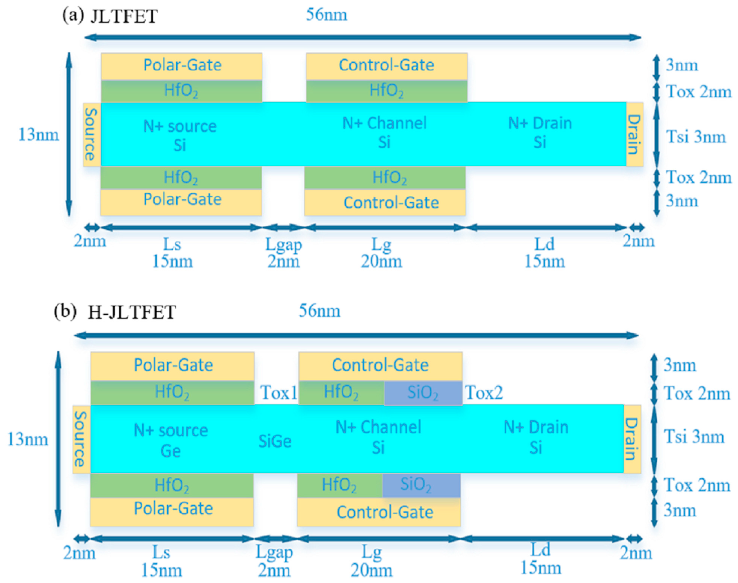
2. Methods
3. Results and Discussion
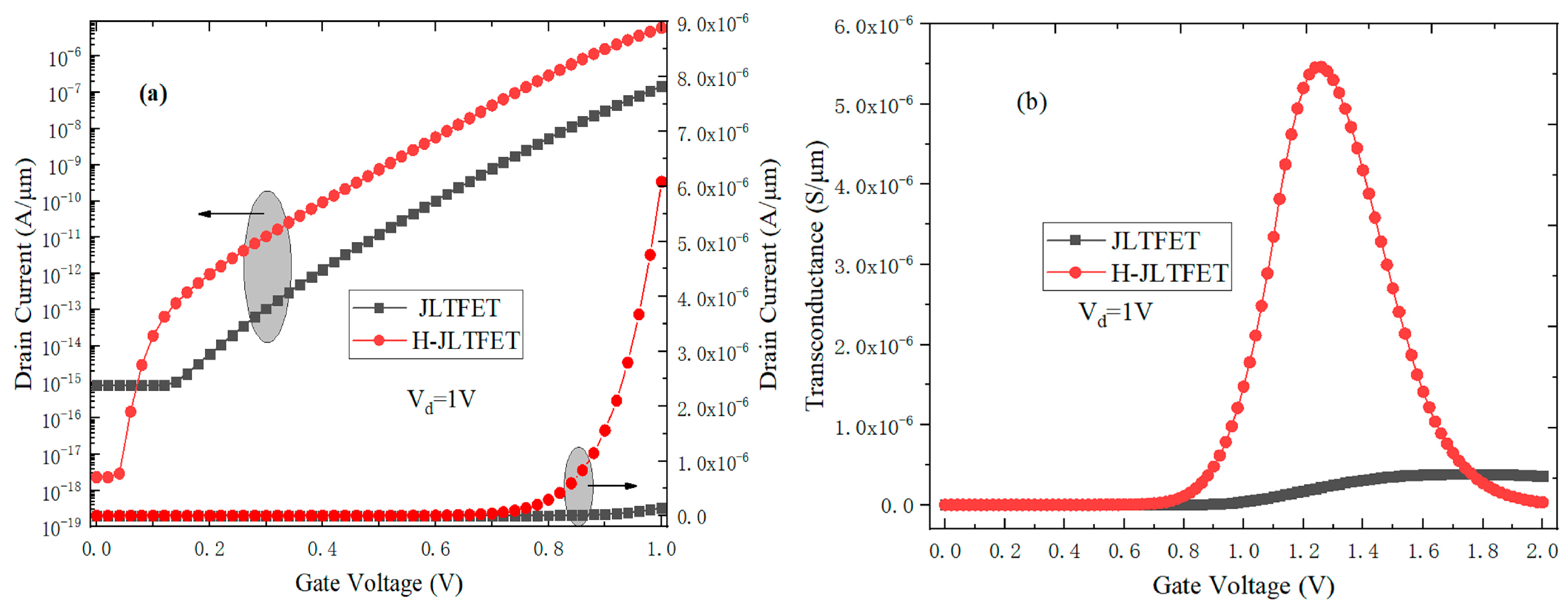
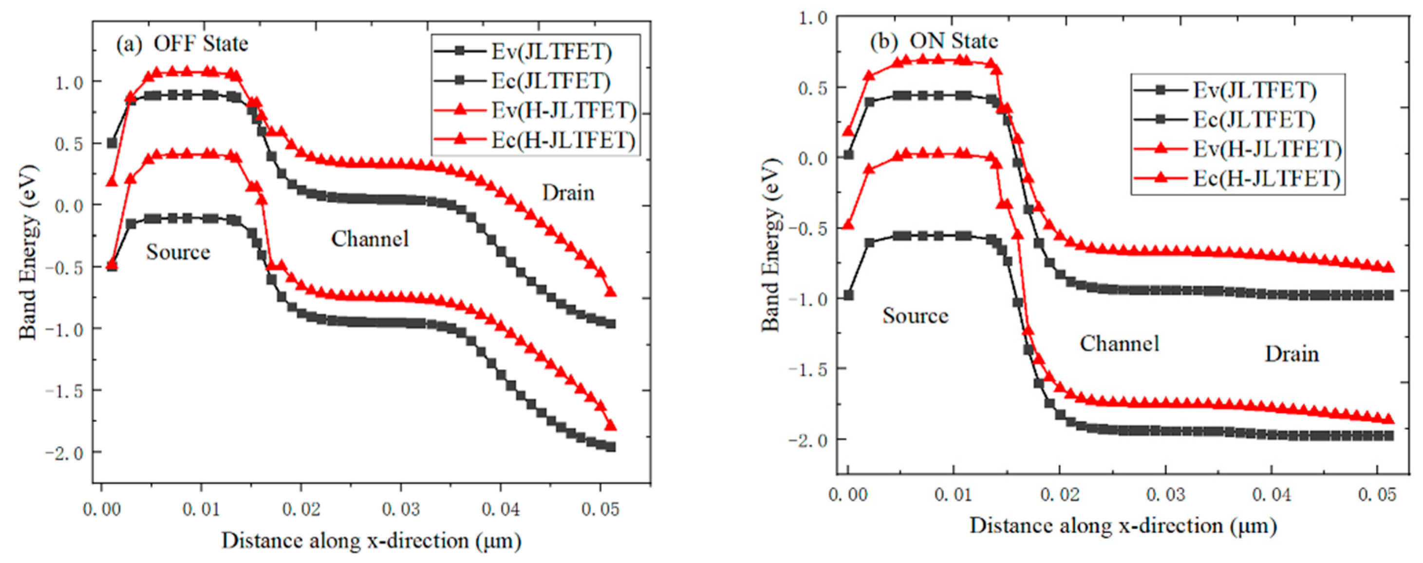
3.1. The Input Characteristics
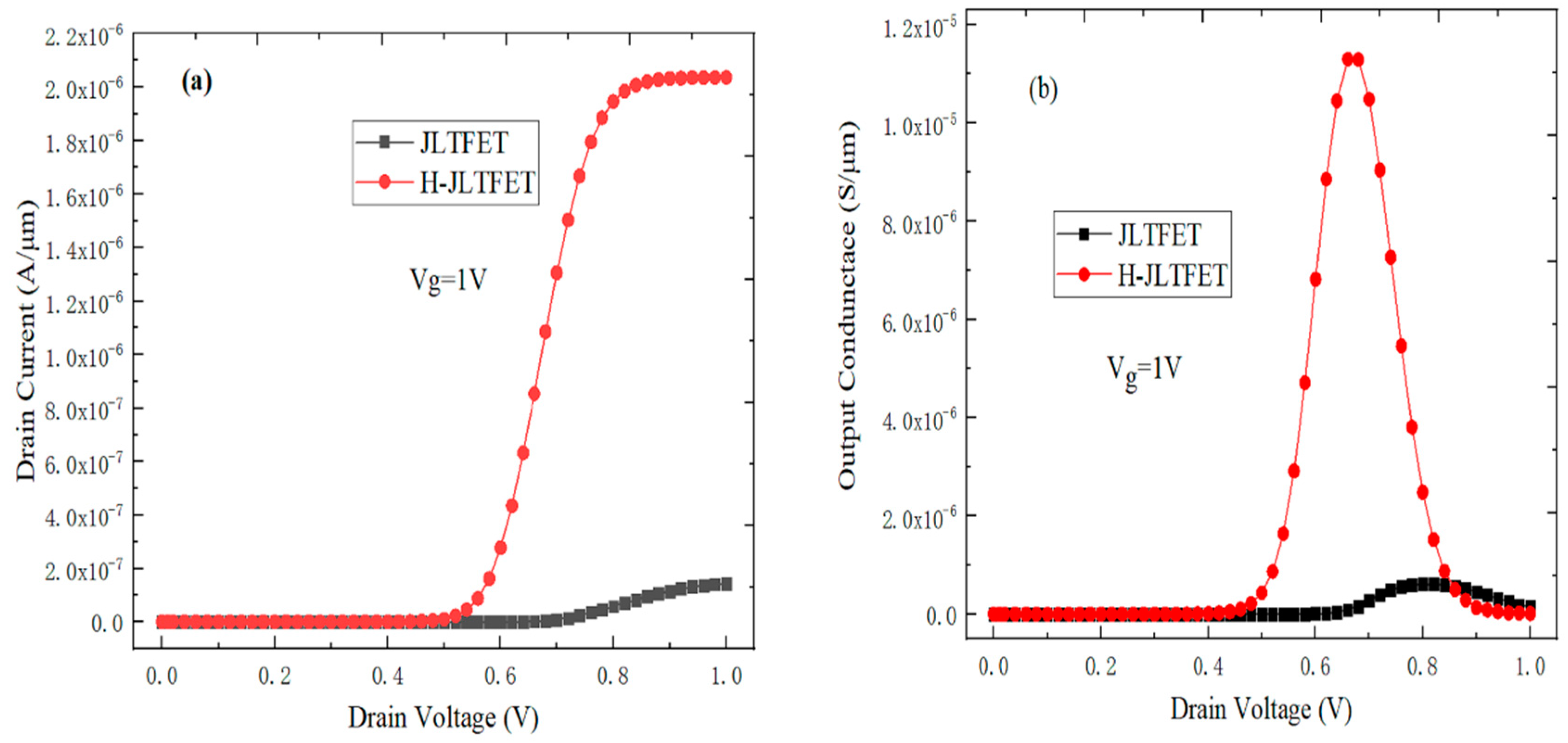
3.2. The Output Characteristics
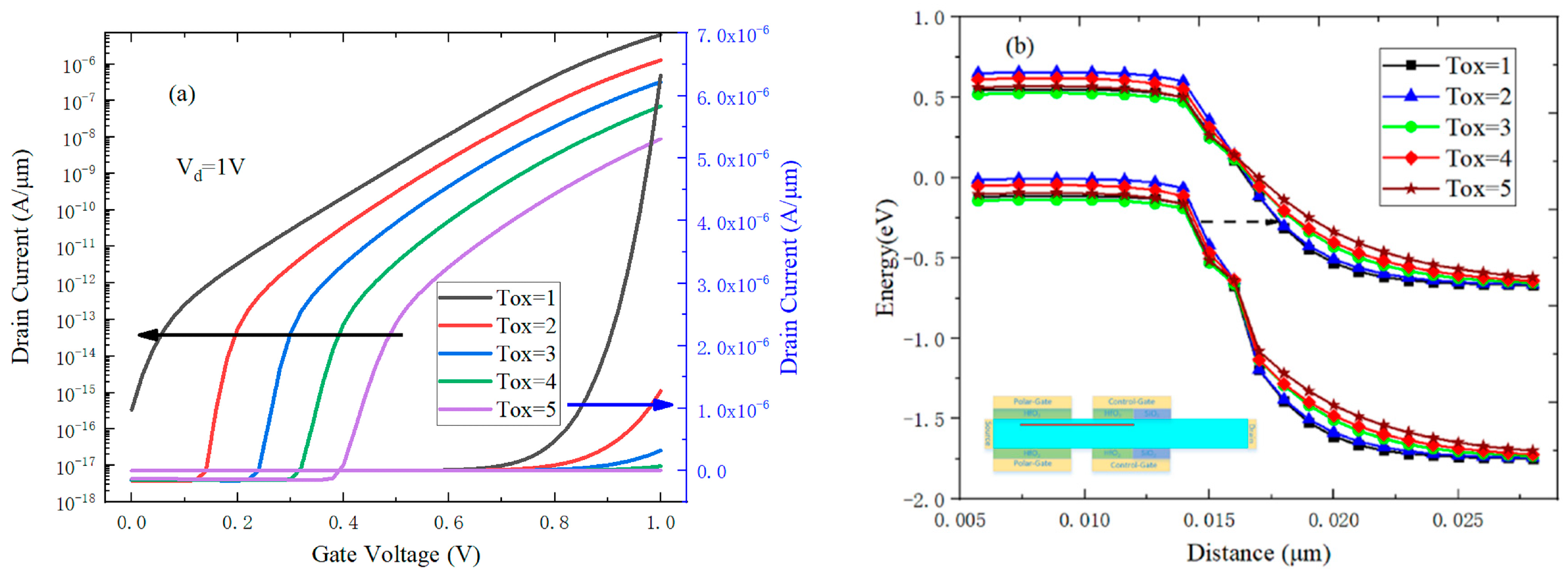
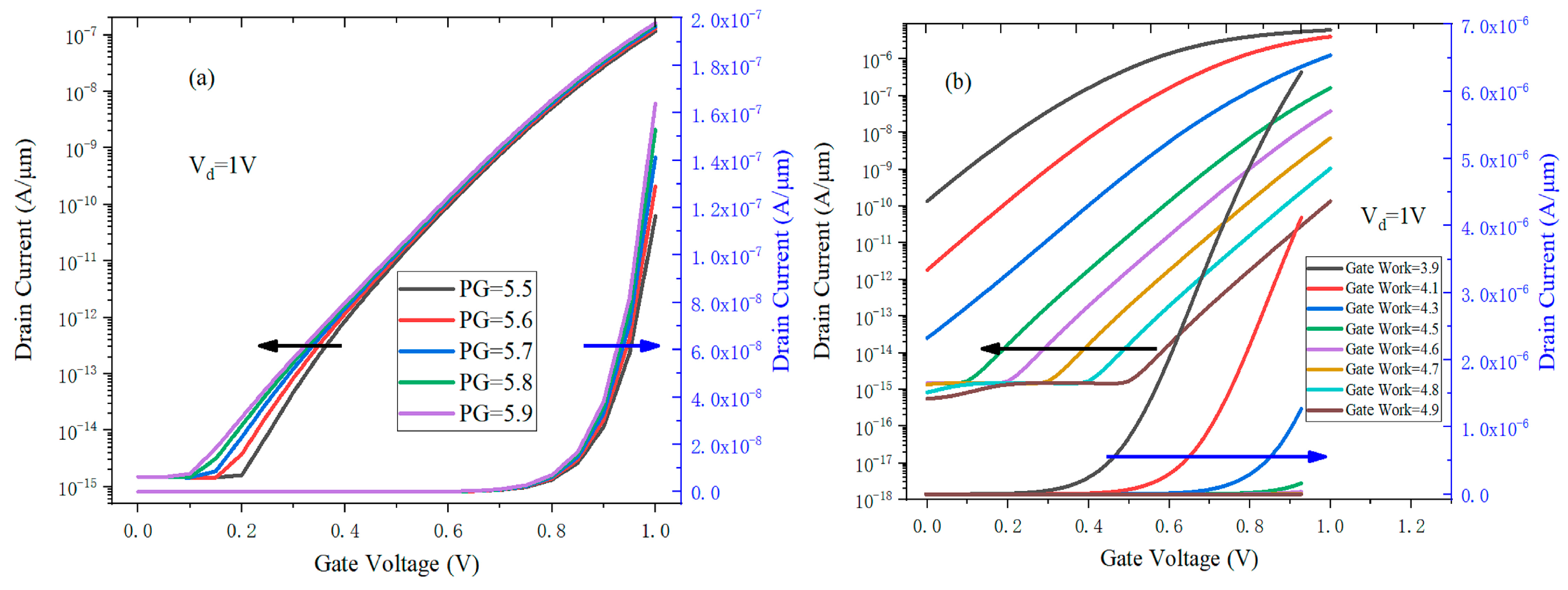
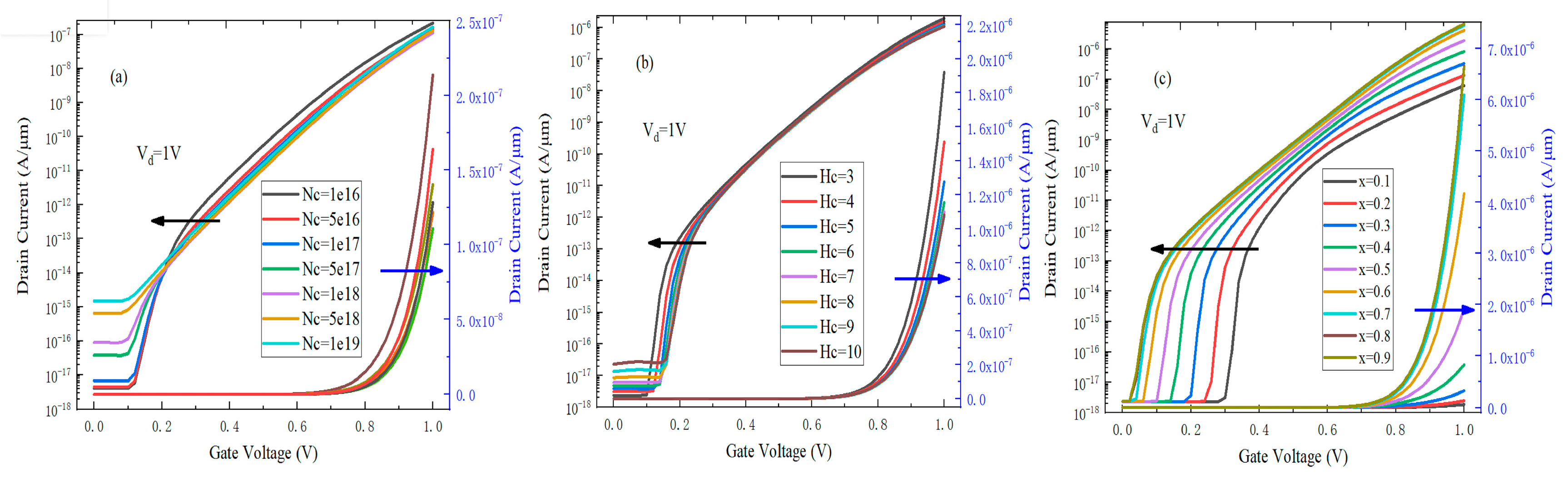
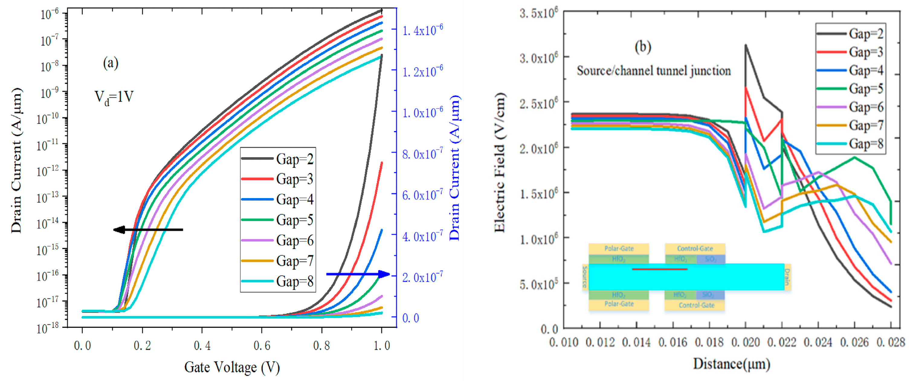
3.3. Effect of Device Sizes on the Transfer Characteristics
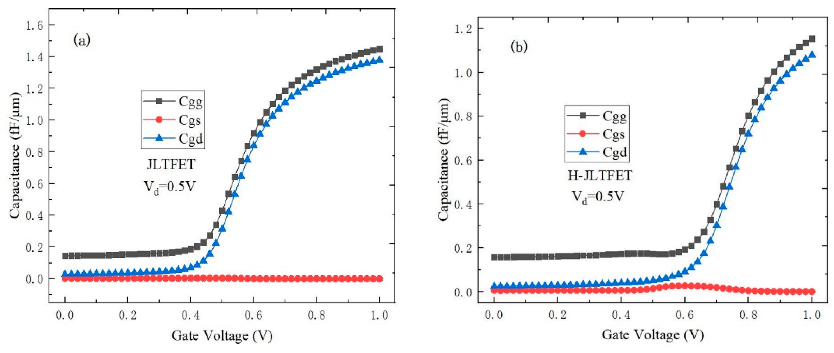
3.4. Capacitance Characteristics
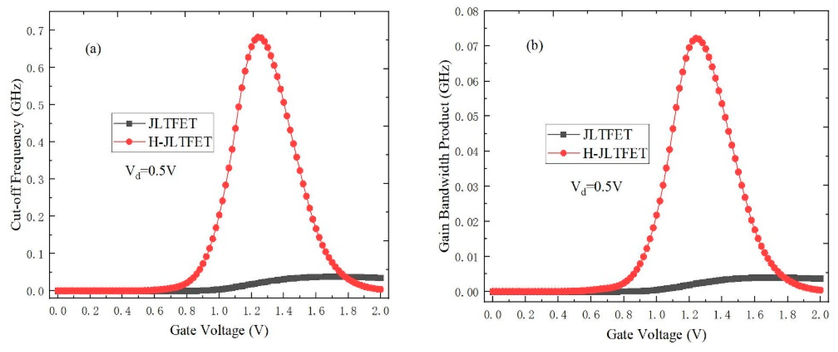
3.5. Frequency Characteristic
4. Conclusions
Author Contributions
Funding
Conflicts of Interest
References
- Basak, S.; Asthana, P.K.; Goswami, Y. Leakage current reduction in junctionless tunnel FET using a lightly doped source. Appl. Phys. A 2015, 118, 1527–1533. [Google Scholar] [CrossRef]
- Singh, D.; Pandey, S.; Nigam, K. A charge-plasma-based dielectric-modulated junctionless TFET for biosensor label-free detection. IEEE Trans. Electron Devices. 2017, 64, 271–278. [Google Scholar] [CrossRef]
- Bal, P.; Akram, M.W.; Mondal, P. Performance estimation of sub-30 nm junctionless tunnel FET (JLTFET). J. Comput. Electron. 2013, 12, 782–789. [Google Scholar] [CrossRef]
- Ghosh, B.; Akram, M.W. Junctionless tunnel field effect transistor. IEEE Electron Device Lett. 2013, 34, 584–586. [Google Scholar] [CrossRef]
- Kao, K.H.; Verhulst, A.S.; Vandenberghe, W.G.; Sorée, B.; Magnus, W.; Leonelli, D. Optimization of gate-on-source-only tunnel fets with counter-doped pockets. IEEE Trans Electron Devices. 2012, 69, 2070–2077. [Google Scholar] [CrossRef]
- Asthana, P.K.; Goswami, Y.; Basak, S.; Rahi, S.B.; Ghosh, B. Improved performance of a junctionless tunnel field effect transistor with a Si and SiGe heterostructure for ultra low power applications. RSC Adv. 2015, 5, 48779–48785. [Google Scholar] [CrossRef]
- Kim, S.W.; Kim, J.H.; Liu, T.J.K.; Choi, W.Y.; Park, B.G. Demonstration of L-shaped tunnel field-effect transistors. IEEE Trans Electron Devices 2016, 63, 1774–1778. [Google Scholar] [CrossRef]
- Rahi, S.B.; Asthana, P.; Gupta, S. Heterogate junctionless tunnel field-effect transistor: Future of low-power devices. J. Comput. Electron. 2017, 16, 30–38. [Google Scholar] [CrossRef]
- Li, W.; Liu, H.; Wang, S.; Chen, S. Reduced Miller capacitance in U-shaped channel tunneling FET by introducing heterogeneous gate dielectric. IEEE Electron Device Lett. 2017, 38, 403–406. [Google Scholar] [CrossRef]
- Raushan, M.A.; Alam, N.; Akram, M.W.; Siddiqui, M.J. Impact of asymmetric dual-k spacers on tunnel field effect transistors. J. Comput. Electron. 2018, 17, 756–765. [Google Scholar] [CrossRef]
- Tirkey, S.; Nigam, K.; Pandey, S.; Sharma, D.; Kondekar, P. Investigation of gate material engineering in junctionless TFET to overcome the trade-off between ambipolarity and RF/linearity metrics. Superlattices Microstruct. 2017, 109, 307–315. [Google Scholar]
- Aghandeh, H.; Ziabari, S.A.S. Gate engineered heterostructure junctionless TFET with Gaussian doping profile for ambipolar suppression and electrical performance improvement. Superlattices Microstruct. 2017, 111, 103–114. [Google Scholar] [CrossRef]
- Raushan, M.A.; Alam, N.; Siddiqui, M.J. Performance Enhancement of Junctionless Tunnel Field Effect Transistor Using Dual-k Spacers. J. Nanoelectron. Optoelectron. 2018, 13, 912–920. [Google Scholar] [CrossRef]
- Wadhwa, G.; Raj, B. Label Free Detection of Biomolecules Using Charge-Plasma-Based Gate Underlap Dielectric Modulated Junctionless TFET. J. Electron. Mater. 2018, 47, 4683–4693. [Google Scholar] [CrossRef]
- Rahi, S.B.; Ghosh, B.; Bishnoi, B. Temperature effect on hetero structure junctionless tunnel FET. J. Semicond. 2015, 36, 034002. [Google Scholar] [CrossRef]
- Singh, G.; Amin, S.I.; Anand, S.; Sarin, R.K. Design of Si0.5Ge0.5 based tunnel field effect transistor and its performance evaluation. Superlattices Microstruct. 2016, 92, 143–156. [Google Scholar] [CrossRef]
- Mallik, A.; Chattopadhyay, A.; Guin, S.; Karmakar, A. Impact of a spacer drain overlap on the characteristics of a silicon tunnel field-effect transistor based on vertical tunneling. IEEE Trans. Electron Devices 2013, 60, 935–943. [Google Scholar] [CrossRef]
- Kim, H.W.; Kim, J.H.; Kim, S.W.; Sun, M.C.; Park, E.; Park, B.G. Tunneling fieldeffect transistor with Si/SiGe material for high current drivability. J. Appl. Phys. 2014, 53, 06JE12. [Google Scholar] [CrossRef]
- Vandooren, A.; Leonelli, D.; Rooyackers, R.; Hikavyy, A.; Devriendt, K.; Demand, M.; Loo, R.; Groeseneken, G.; Huyghebaert, C. Analysis of trap-assisted tunneling in vertical Si homo-junction and SiGe hetero-junction tunnel-FETs. Solid State Electron. 2013, 83, 50–55. [Google Scholar] [CrossRef]
- Choi, W.Y.; Lee, H.K. Demonstration of hetero-gate-dielectric tunneling field-effect transistors (HG TFETs). Nano Convergence 2016, 3, 1–15. [Google Scholar] [CrossRef]
- ATHENA/ATLAS User’s Manual; SILVACO International: Santa Clara, CA, USA, 2012.
- Ionescu, M.; Riel, H. Tunnel field-effect transistors as energy-efficient electronic switches. Nature 2011, 479, 329–337. [Google Scholar] [CrossRef]
- Chen, S.; Wang, S.; Liu, H.; Li, W.; Wang, Q.; Wang, X. Symmetric U-shaped gate tunnel field-effect transistor. IEEE Trans. Electron Devices 2017, 64, 1343–1349. [Google Scholar] [CrossRef]
- Avci, U.E.; Young, I.A. Heterojunction TFET scaling and resonant-TFET for steep subthreshold slope at sub-9nm gate-length. In Proceedings of the 2013 IEEE International Electron Devices Meeting, Washington, DC, USA, 9–11 December 2013. [Google Scholar]
- Wang, Q.; Wang, S.; Liu, H.; Li, W.; Chen, S. Analog/RF performance of L-and U-shaped channel tunneling field-effect transistors and their application as digital inverters. Jpn. J. Appl. Phys. 2017, 56, 064102. [Google Scholar] [CrossRef]
- Cao, W.; Yao, C.J.; Jiao, G.F.; Huang, D.; Yu, H.Y.; Li, M.F. Improvement in reliability of tunneling field-effect transistor with pnin structure. IEEE Trans. Electron Devices 2011, 58, 2122–2126. [Google Scholar] [CrossRef]
- Wang, W.; Wang, P.F.; Zhang, C.M.; Lin, X.; Liu, X.Y.; Sun, Q.Q.; Zhou, P.; Zhang, D.W. Design of U-shape channel tunnel FETs with SiGe source regions. IEEE Trans. Electron Devices 2014, 61, 193–197. [Google Scholar] [CrossRef]


© 2019 by the authors. Licensee MDPI, Basel, Switzerland. This article is an open access article distributed under the terms and conditions of the Creative Commons Attribution (CC BY) license (http://creativecommons.org/licenses/by/4.0/).
Share and Cite
Han, T.; Liu, H.; Wang, S.; Chen, S.; Li, W.; Yang, X.; Cai, M.; Yang, K. Design and Investigation of the Junction-Less TFET with Ge/Si0.3Ge0.7/Si Heterojunction and Heterogeneous Gate Dielectric. Electronics 2019, 8, 476. https://doi.org/10.3390/electronics8050476
Han T, Liu H, Wang S, Chen S, Li W, Yang X, Cai M, Yang K. Design and Investigation of the Junction-Less TFET with Ge/Si0.3Ge0.7/Si Heterojunction and Heterogeneous Gate Dielectric. Electronics. 2019; 8(5):476. https://doi.org/10.3390/electronics8050476
Chicago/Turabian StyleHan, Tao, Hongxia Liu, Shulong Wang, Shupeng Chen, Wei Li, Xiaoli Yang, Ming Cai, and Kun Yang. 2019. "Design and Investigation of the Junction-Less TFET with Ge/Si0.3Ge0.7/Si Heterojunction and Heterogeneous Gate Dielectric" Electronics 8, no. 5: 476. https://doi.org/10.3390/electronics8050476
APA StyleHan, T., Liu, H., Wang, S., Chen, S., Li, W., Yang, X., Cai, M., & Yang, K. (2019). Design and Investigation of the Junction-Less TFET with Ge/Si0.3Ge0.7/Si Heterojunction and Heterogeneous Gate Dielectric. Electronics, 8(5), 476. https://doi.org/10.3390/electronics8050476