Article

Analysis of Memory Matrices with HfO2 Memristors in a PSpice Environment

Department Theoretical Electrical Engineering, Technical University of Sofia, 1000 Sofia, Bulgaria
Electronics 2019, 8(4), 383; https://doi.org/10.3390/electronics8040383
Submission received: 1 March 2019 / Revised: 15 March 2019 / Accepted: 27 March 2019 / Published: 29 March 2019
(This article belongs to the Section Circuit and Signal Processing)

Abstract

:
The investigation of new memory circuits is very important for the development of future generations’ non-volatile and Random Access Memories (RAM) memories and modern schemes for in-memory calculations. The purpose of the present research is to propose a detailed analysis of passive and hybrid memristor-based memory crossbars with separating metal oxide semiconductor (MOS) transistors. The considered memristors are based on HfO2. The transistors are applied to eliminate the parasitic paths in the schemes. For simulations, a previously proposed strongly nonlinear modified window function by the author together with a physical nonlinear memristor model is used. The considered model is adjusted according to the experimental i–v relationship of HfO2 memristors. The i–v relationship obtained by the simulation is successfully fitted to the respective relationship derived by physical measurements. A good coincidence between these characteristics is established. Several basic window functions are also applied for comparison to the corresponding results. The proposed model is analyzed in Personal Simulation Program with Integrated Circuit Emphasis (PSpice) and it is also used for simulation of a 5 × 5 fragment of a memristor memory crossbar with isolating transistors and for the analysis of a 6 × 6 passive memory matrix. The investigated matrices are simulated for writing, reading, and erasing information. It is established that the model proposed could be used for simulations of complex memristor circuits.

1. Introduction

The resistance-switching effect, observed in many amorphous oxides (TiO2, HfO2 and others), has been analyzed since 1970 [1,2]. It has been established that such oxides have the capability to alter their resistance in accordance to the applied voltage and to retain their state for a long time period [1,2]. Analogous behavior was forecast for the memristor by Chua in 1971 [3]. The memristor is an important two-terminal element together with the resistor, inductor, and capacitor [1,2,3]. The memristor is a strongly nonlinear component [3,4]. It relates the charge q and the flux linkage Ψ [3,4]. The memristor, in accordance to symmetry considerations and the relationships between the essential electric quantities (current, voltage, charge and flux linkage), was predicted by Chua in 1971 [3,4]. The memristor has the capability to remember the electric charge passed through it, when the sources are switched off [3,4,5]. Its current-voltage relationship is a pinched-hysteresis loop, whose shape and range depend on both the amplitude and the frequency of the used signal [3,4]. Since the memristor can retain its resistance after turning the sources off, it can be applied as a non-volatile memory component [4,5,6]. Its physical realization by HfO2, TiO2 or other modern amorphous metal-oxide materials [5,6,7,8] has geometrical sizes in the nano-range and its power consumption is many times lower than traditional flash memory elements and conventional random access memory (RAM) devices [5,6,7]. These indications are good fundamentals for future applications of memristor crossbars in high-density memories [9,10,11,12].
In-memory computing with memristors is a very important and valuable technique for future generation’s memories and computational circuits [13,14,15]. This paper and a previous one written by the author [16] are associated with in-memory calculation circuits and memory devices based on memristors. The previous paper [16] considers an analysis of the crossbar with four transistors and four resistance-switching memory elements 4T4R matrix with TiO2 memristors in MATrix Laboratory (MATLAB). The present research is an attempt to analyze memristor crossbars (10T25R) with different types of memristors—HfO2-based memory elements, which are modern and important for new engineering applications. This investigation is realized in the PSpice environment by applying different memristor models. An additional comparison between the applied parameters is made. The first physical memristor was created in the Hewlett Packard (HP) research laboratories by Williams’s scientific team in 2008 [4]. A number of papers related to memristors and memristive devices have been published and many models have been proposed [5,6,7,9]. The linear dopant drift model [4] is applied for low-level signals. The nonlinear models proposed by Biolek [6] and Joglekar [5] are able to illustrate nonlinear memristor performance for high-level signals and low frequencies according to the state variable [9]. The Pickett model [17] is based on physical measurements, and on the mechanism of the current flow through a tunnel barrier. It has maximal correctness and at times it is used as a standard reference model [9,17]. Unfortunately, it is very complex and it is not appropriate for computer simulations due to convergence problems [10,18]. The boundary condition memristor (BCM) model [9] is combined with a linear ionic dopant drift and a switch-based algorithm to describe several boundary effects. Regrettably, several basic linear memristor models, such as Joglekar [5], Biolek [6] and BCM [9], are appropriate for circuit analysis when the memristor voltage is lower than 1 V and the practically observed switching effects for voltages higher than 1.5 V cannot be correctly described. For these models [5,6,9], nonlinearity is associated only to the memristor state variable. The interest in the present investigation is related to modern and not very well analyzed types of memristors, based on transition-metal oxide materials, such as HfO2 [7,8,19]. Several basic models of HfO2 memristors exist in the technical literature [7,8]. Some of them, such as the model proposed by Lupo et al. [7], are either complex or not very accurate, such as the memristor model proposed by Amer et al. [8]. Others, such as Biolek [6] and Joglekar [5], are not capable of precisely expressing the respective i–v relationships, due to the low nonlinearity of the describing mathematical i–v relationship. The Lehtonen-Laiho memristor model [20,21] is based on physical experiments, and on the mechanism of the current flow through semiconducting amorphous transition-metal oxides [20]. It has good precision and a tunable mathematical expression [20,21]. This model is applied in the present research after adjustment according to the experimental i–v characteristic of HfO2 memristors [8]. The memristor memory technology and the associated in-memory computing are promising ones, which could potentially replace conventional memory and computational circuits [22,23,24,25]. Memristors are used in memories as a storing element [24,26,27]. Metal oxide semiconductor (MOS) transistors are applied in hybrid resistance-switching circuits to eliminate existing sneak paths [24]. To the best of the author’s knowledge, there is a certain absence of detailed results acquired by memristor memory physical measurements and simulations with the fundamental models. The motivation for the present research is to partially fill this absence and to propose additional and detailed research of fragments of a hybrid memory, containing the fundamental electric elements for the basic writing and reading procedures: Word lines, bit lines, write enable, and read enable lines; 25 memristors; 10 separating transistors; and of a passive memristor circuit. For these analyses, a highly nonlinear model [20,21] together with several basic window functions and a modified by the author window function [25] will be applied. A comparison to experimental data [8] and between the results from different models will also be made. The ability of the model [20,21], together with the modified window function [25], for realistic representation of the performance of complex memristor devices will be established.
The paper is organized as follows. A short description of several mathematical memristor models applied for the analysis of memory fragments and their adjustment according to experimental the HfO2-memristor i–v relationship are presented in Section 2. The corresponding PSpice memristor models based on the described mathematical models are shown in Section 3. The investigation of a hybrid matrix based on the used models is realized in PSpice and is described in Section 4. An analysis of a passive memristor crossbar is presented on Section 5. The concluding remarks are included in Section 6.

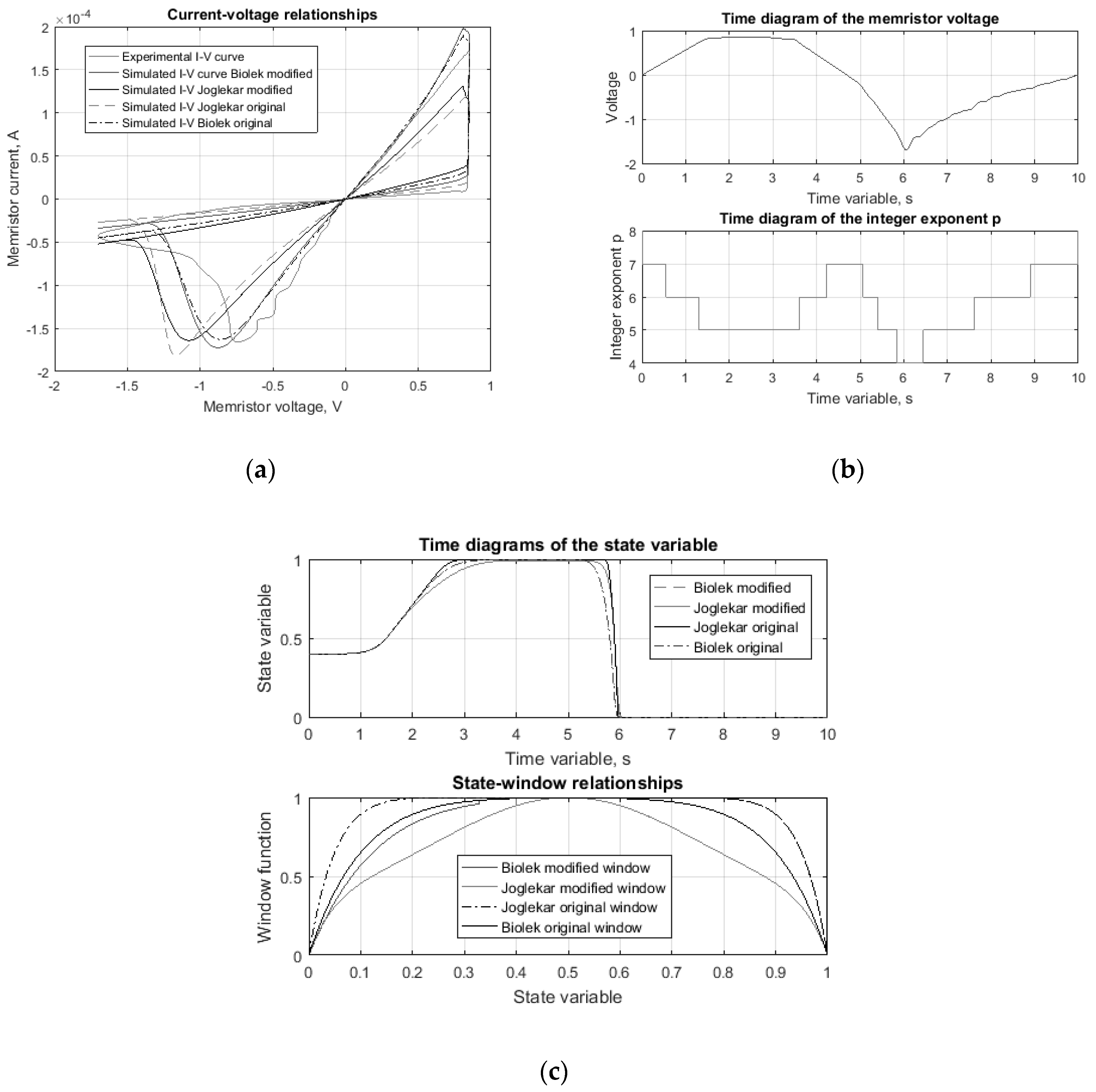
2. A Brief Overview of the Applied Memristor Mathematical Models

In this section, four mathematical memristor models based on the Lehtonen-Laiho model will be described. Two of them use the standard Joglekar [5] and Biolek [6] window functions, respectively. The other two models use modified Joglekar and Biolek window functions [25].
In [20,21], a physics-based model for transition-metal oxide memristors was presented. It is based on experimental data [20,21]. The approximated relationship between the memristor current, i and the voltage, v [16,17], is expressed by Equation (1):
i = x n β sinh ( α v ) + χ [ exp ( γ v ) 1 ]
where the variables, n, β, α, χ and γ, are fitting parameters [20,21], and i and v are the memristor current and voltage, respectively. In this model [20,21], the state variable, x, is a normalized factor in the interval [0,1]. This model represents an asymmetric behavior. When the memristor is in the closed ON state, the state variable is near to unity and the current is mainly dominated by the first term in Equation (1), which illustrates a tunneling effect [20,21]. When the memristor element is in the open OFF state, the state variable is near zero and the current is mainly expressed by the second term in Equation (1), which represents a rectifying diode equation [20,21]. The applied memristor model [20,21] uses a nonlinear dependence on voltage in the state differential equation [20,21]—Equation (2):
d x d t = a × f ( x ) × v s
where a is a constant, s is an odd integer exponent, and f(x) is a window function used for approximate representation of the nonlinear ionic dopant drift and the limitation boundary effects [20,21]. The window function introduces nonlinearity according to the state variable of the memristor [18]. Equations (1) and (2) determine the respective physical memristor model [18,20]. The electric charge transport in the memristor is related to the ionic drift in the considered oxide medium [1,2,18]. The ions move between two adjacent positions via a migration barrier [18,20]. This potential barrier could be lowered by the applied electric field [1,2,20]. The charged particles can obtain more thermal energy by Joule heating in a set of definite oxide materials and can hence easily overcome the tunnel barrier [1,2,18]. The nonlinearity of the dopant motion starts from local heating in a group of specific material media, or from high electric fields [1,2,18,20]. In the present investigation, several different window functions are used [5,6,25]. They are briefly discussed below. A frequently used window function proposed by Biolek in [6] is:
f B ( x , i ) = 1 [ x s t p ( i ) ] 2 p
where p is a positive integer exponent and the relay function, stp, is expressed as follows:
s t p ( i ) = { 1 , i f   i 0 ( v 0 ) 0 , i f   i < 0 ( v < 0 )
The Biolek window function could also be expressed as follows [6]:
f B ( x , v ) = 1 ( x 1 ) 2 p , v 0 f B ( x , v ) = 1 x 2 p , v > 0
The Lehtonen-Laiho model [20,21], in combination with the original Biolek window function [6], could be presented by the following system of equations:
i = x n β sinh ( α v ) + χ [ exp ( γ v ) 1 ] d x d t = a × { 1 [ x s t p ( i ) ] 2 p } × v s
Another commonly used window function is the so called Joglekar window, fJ [5]:
f J ( x ) = 1 [ 2 x 1 ] 2 p
The Lehtonen-Laiho nonlinear memristor model [20,21], in combination with the Joglekar window [5], is:
i = x n β sinh ( α v ) + χ [ exp ( γ v ) 1 ] d x d t = a × [ 1 ( 2 x 1 ) 2 p ] × v s
In [25], the original Biolek window function is modified and the positive integer exponent, p, is a function of the applied voltage:
p = r o u n d ( b | v | + c )
where b and c are fitting parameters and the function, ‘round’, is used to derive an integer result [28]. The window function modified by the author, fBM [25], is:
f B M ( x , v ) = 1 ( x 1 ) 2   r o u n d ( b | v | + c ) , v 0 f B M ( x , v ) = 1 x 2   r o u n d ( b | v | + c ) , v > 0
The considered highly-nonlinear memristor model [20,21] together with the previous strongly nonlinear modified window function proposed by the author (10) [25] is:
| i = x n β sinh ( α v ) + χ [ exp ( γ v ) 1 ] d x d t = a · [ 1 ( x 1 ) 2   r o u n d ( b | v | + c ) ] · v s , v v t h r d x d t = a · [ 1 x 2   r o u n d ( b | v | + c ) ] · v s , v > v t h r d x d t = 0 , v t h r < v v t h r
where vthr is an activation threshold. Another highly nonlinear window function, proposed here by the author, is:
f M O D ( x ) = d × f J ( x ) + g × sin 2 ( π x ) d + g
where fJ is expressed with (7). This window function has increased nonlinearity with respect to the corresponding original Joglekar window function [5] and its usage leads to an increase of the nonlinearity of the ionic dopant representation. The respective Lehtonen-Laiho model [20,21] in combination with the proposed highly-nonlinear window function expressed with (12) is:
i = x n β sinh ( α v ) + χ [ exp ( γ v ) 1 ] d x d t = a × [ d × f J ( x ) + g × sin 2 ( π x ) d + g ] × v s
where d = 4.5 and g = 5.5 are fitting parameters. The Lehtonen-Laiho memristor model [20,21] is adjusted according to the experimental current-voltage characteristic of the HfO2 memristor [8]. Figure 1a, containing the experimental i–v relationship and the respective simulated characteristics of the hafnium dioxide memristor, is presented for comparison with the results derived in MATLAB (MathWorks, Natick, MA, USA) [28].
The simulated current-voltage curves are derived by the use of the Lehtonen-Laiho model [20,21] together with the window functions described above—Equations (6), (8), (11) and (13). The modified Joglekar and Biolek window functions together with the used model ensure best proximity between the simulated and the experimental i–v relationship of the memristor. The proximity between the derived characteristics depends mainly on the current-voltage relation in the Lehtonen-Laiho model [20,21]. The influence of the used window functions is associated only to the respective state variable and it is not strongly expressed during the simulations. The time diagram of the corresponding voltage signal used for deriving the current-voltage characteristics is presented in Figure 1b for illustration of its magnitude and shape. The corresponding change of the positive integer exponent in Equation (11) in the time domain is also shown Figure 1b for confirmation of the ability of the applied modified Biolek window function to change the exponent in accordance to the memristor voltage and the following change of state variable. The corresponding change of the memristor state variable, x, in the time domain is presented in Figure 1c to illustrate the change of the memristor state in accordance to the applied voltage. It is visible that these curves almost match each other, and one could conclude that the used window function does not strongly affect the respective memristor state variable. The respective window functions of the applied models are presented in Figure 1c for illustration of their different nonlinearity with respect to the memristor state variable. The modified Biolek and Joglekar window functions have different nonlinearity according to the applied memristor voltage. It is obvious that the proposed Joglekar modified window function has the highest nonlinearity. The values of the fitting coefficients used in the Lehtonen-Laiho model are presented in Table 1 for application in the next PSpice memristor models. These values are approximately expressed, and they depend on the simulation conditions—signal amplitude, frequency, and the electric mode.

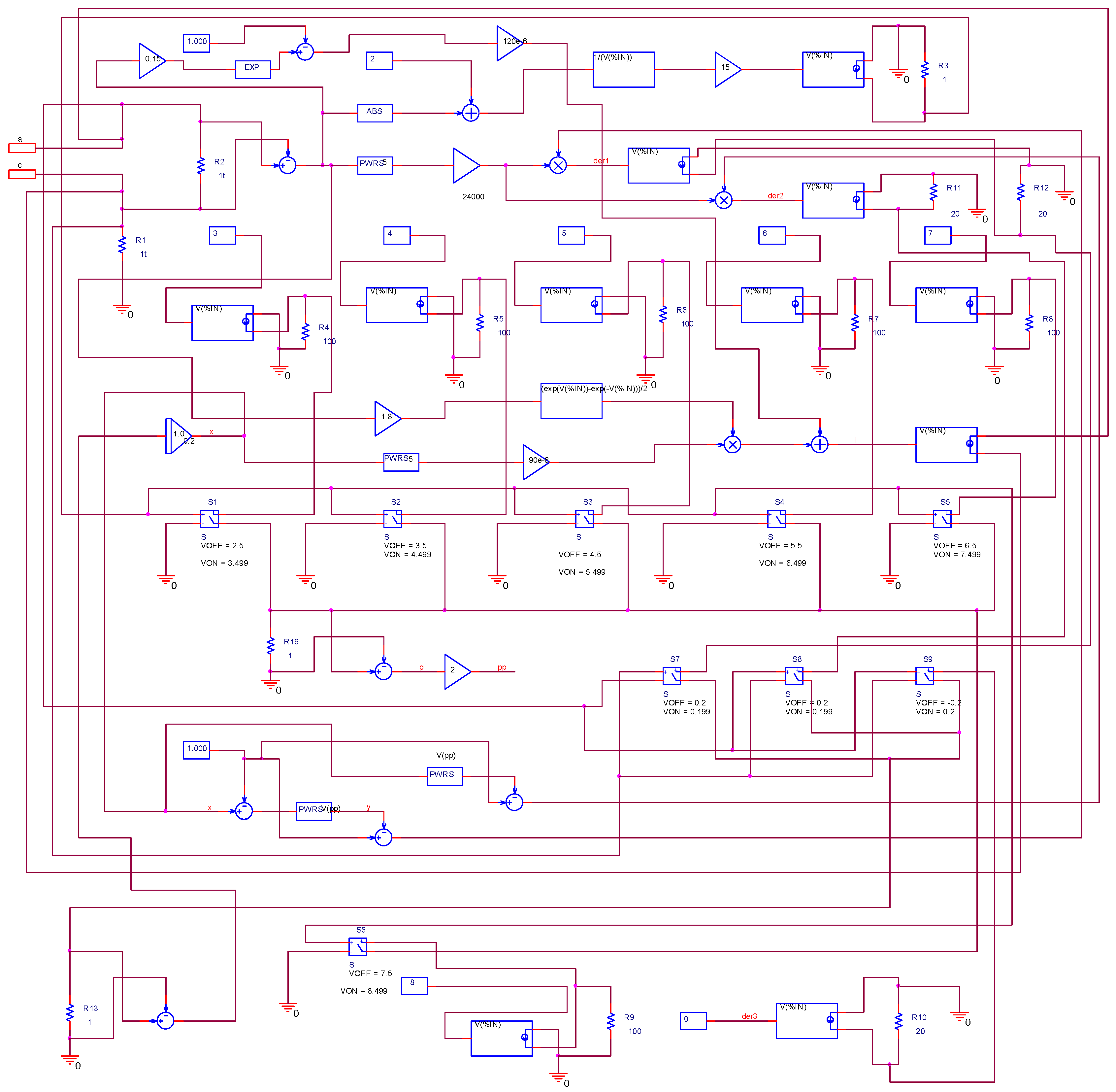
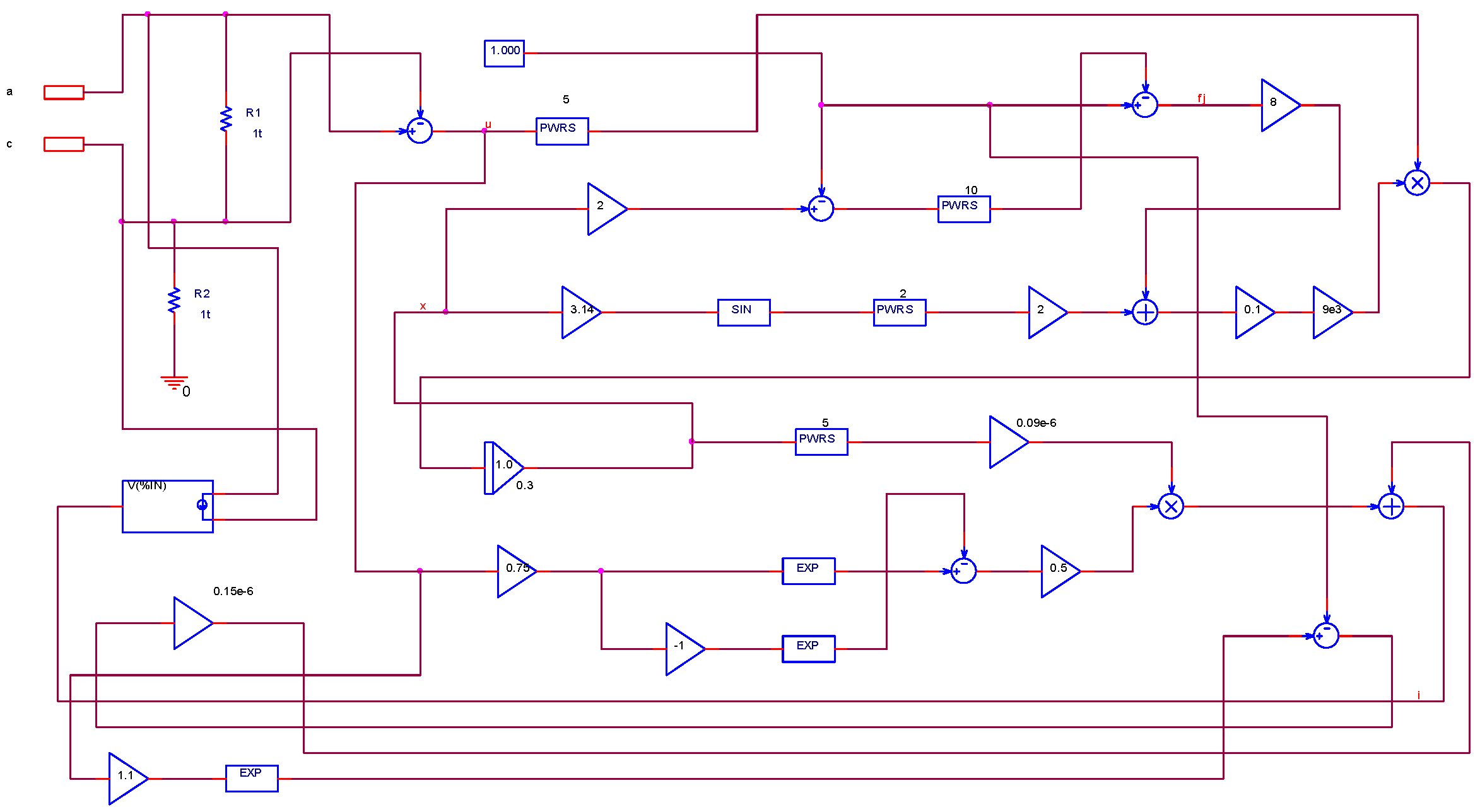
3. PSpice Memristor Models

Using the mathematical memristor models described in the previous section and presented by Equations (6), (8), (11) and (13), respective PSpice memristor models were derived and saved in external PSpice libraries. The creation of the respective PSpice memristor schematic starts from the state variable, x, existing in the corresponding window function. After expressing the mathematical operations according to the respective equation, the obtained signal for the time derivative of the state variable is integrated and then it is substituted in the first equation of the Lehtonen-Laiho memristor model [20,21]. The corresponding schematic of the PSpice memristor model according to Equation (11) is presented in Figure 2 for visualization of its structure and further derivation of the PSpice output file. The electrodes of the equivalent memristor are denoted by the anode (a) and cathode (c).
The respective PSpice [29] model of the schematic presented in Figure 2 [25] is given in Appendix A for the application in the external PSpice library memristor element. The schematic of the model, expressed by Equation (13), is presented in Figure 3 for illustration of the basics of the proposed memristor model in the PSpice [25] environment. Its creation is similar to the model discussed above [21]. The memristor terminals are denoted as the anode (a) and cathode (c).
The corresponding PSpice [25] model according to Equation (13), presented for application in a PSpice library element, is given in Appendix B.

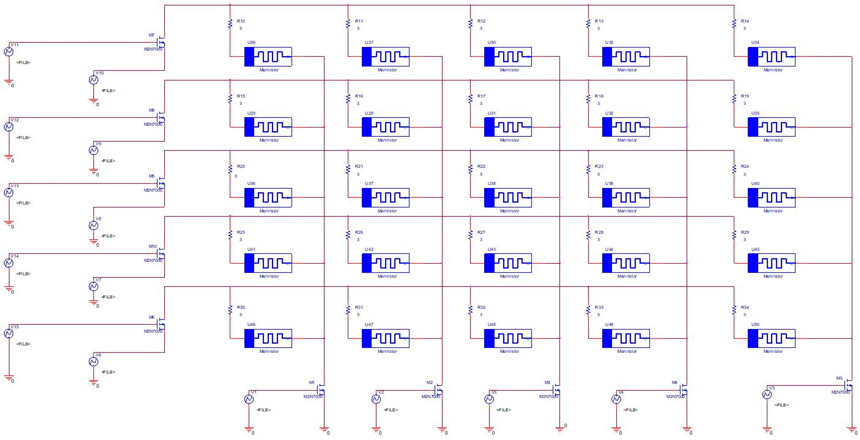
4. PSpice Analysis of a Hybrid Memristor Memory Crossbar

A resistance-switching memory scheme with 25 memristors and 10 separating MOS transistors according to [24] is presented in PSpice in Figure 4 to illustrate the following description of the applied signals for writing and reading processes. The applied basic simulation parameters are: tmax = 12 µs, time step size: 0.18 ns, and default nominal temperature: 27 °C. Writing a logical unity in a memristor cell is realized by applying a voltage pulse with a positive polarity, duration of 1 µs, and a level of 2 V. In the end of the applied impulse, the state and the respective resistance of the memristor are changed to values corresponding to its ON state. Writing a logical zero is made by a negative voltage pulse with the same duration and at the end of this operation the memristor is operating in a mode near to its OFF state. Selecting the corresponding memory cell enables storing a bit of information, i.e., logical unity or logical zero in the memristor element [11,22,24]. Reading the information stored in the respective memristor is realized by applying a voltage pulse with a duration of 1 µs and a level of 0.1 V. Due to the low level of the signal, the memristor state is not changed and its stored information is unaffected. An additional resistor connected in series to the respective memristor and sense amplifier is used for reading information. The signal proportional to the logical unity is about 0.3 V and for logical zero, it is around 0.01 V. MOS transistors are applied for interruption of the parasitic sneak paths between the bit lines and the corresponding word lines [24]. The “write enable” and “read enable” signals are additional ones and they are be applied to the gate electrodes of the corresponding MOS transistors. Then, the desired memory element can be selected [22,24]. If the respective MOS transistor operates in a cut-off mode, it stops the respective parasitic current and the related sneak path. The potentials of the source electrodes of the MOS transistors, M1 and M6, needed for writing and reading logical information, are pulses with different levels. In the first 1 µs, a logical unity is stored in the memristor cell, M11, and its resistance is decreased to the minimal value—2kΩ. In the next 1 µs, a logical zero is stored in the memory cell, M11, and the memristance is increased to the maximal value—500kΩ. In the following 1 µs, a reading voltage impulse with a low level (0.1 V) is applied to the corresponding memristor. The write-enable and read-enable signals applied to the gate electrodes of the MOS transistors, M1 and M6, are also impulses with different levels. To select the memristor element, M11, positive potentials with a value of 2 V must be applied to the gates of both transistors, M1 and M6, with respect to their sources. The time diagrams of the memristor voltage and the corresponding state variable and memristance of M11 acquired during the memory circuit investigation is shown in Figure 5 for illustration of the change of the memristor’s resistance and its OFF to ON and ON to OFF switching for the applied memristor models. The respective diagrams are derived for different voltages and frequencies with respect to those presented in Figure 1 and they are similar to one another. The corresponding current-voltage characteristics of the memristors derived during the operation of the memory scheme are presented in Figure 6 for illustration of the ability of the applied memristor models and the respective window functions [5,6,20,21,25] to operate in memory circuits. The little difference between these characteristics could be explained by the dissimilarity in the initial values of the corresponding memristor state variables. These i–v relations are very close to each other. According to the model with the modified Biolek window function, the current changes in a larger range, which leads to a broad change of the memristance and better recognition of the logical levels. The resistance of the memristor element alters in a broad range. After comparison of the i–v relationships of the memristor element derived by the use of the applied modified models [21] with the experimental current-voltage characteristics [8] derived for similar conditions, a good similarity between them is established. The broad interval of changing the memristance is a useful phenomenon for the precise differentiation the logical levels. It could be concluded that the used nonlinear memristor models with modified window functions could be applied to investigate a large number of complex memristor circuits and devices. An advantage of the memristor model [20,21] with the modified window functions [25] used here, compared to several existing linear models—e.g., BCM [9], Biolek [6] and Joglekar [5] models—is the realistic representation of the high nonlinearity of the exponential ionic dopant drift for high-level voltage signals [20,21] and the observed switching phenomenon. The resistances of the word lines and bit lines have a value of 3 Ω and are represented by respective resistors connected with the memristors in series connection. After analysis of the results (time diagrams of the memristor state variable and resistance change), it was established that due to the very low resistance of the word lines and the bit lines with respect to the memristance in its whole range, the considered additional resistance does not affect the normal operation of the circuit.

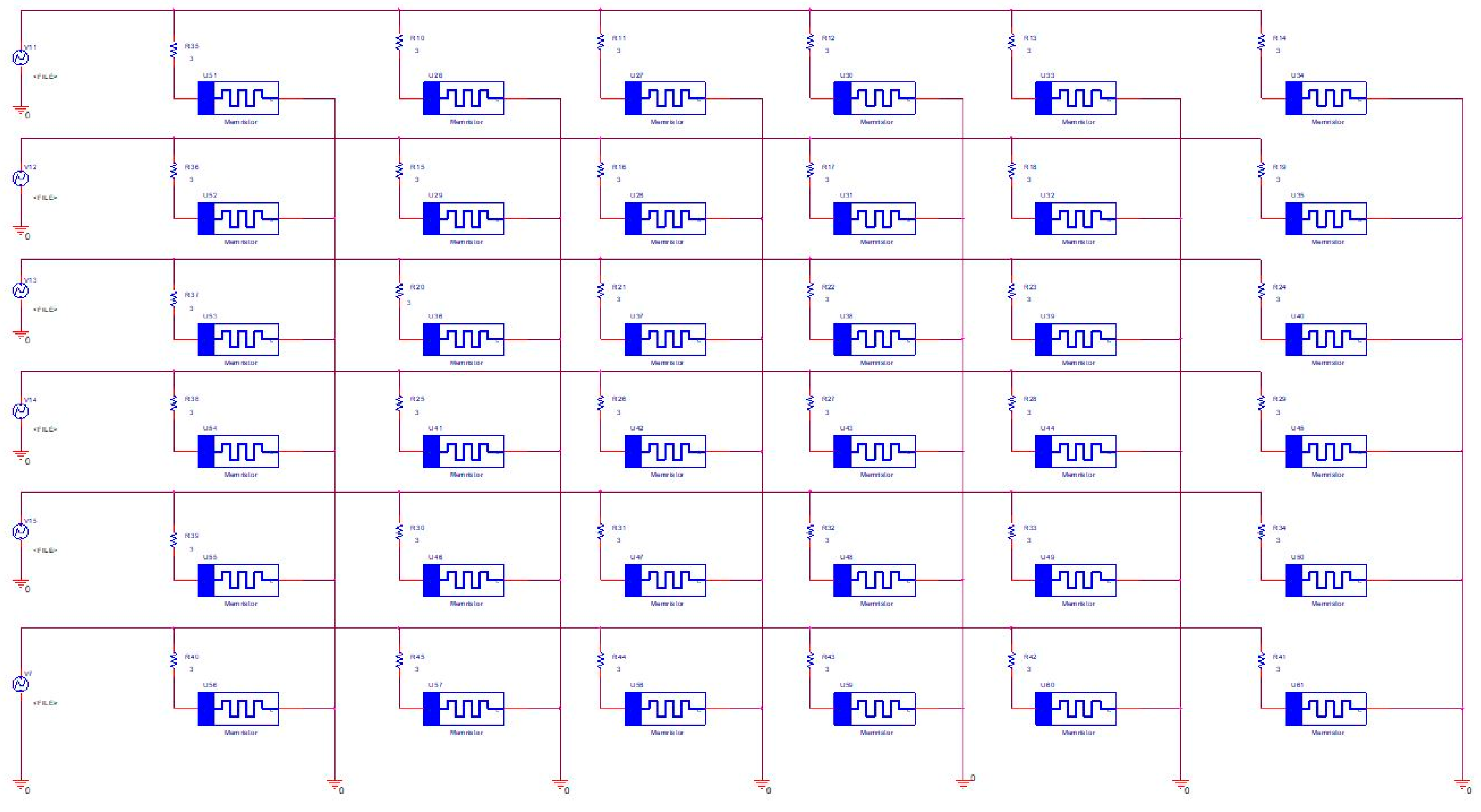
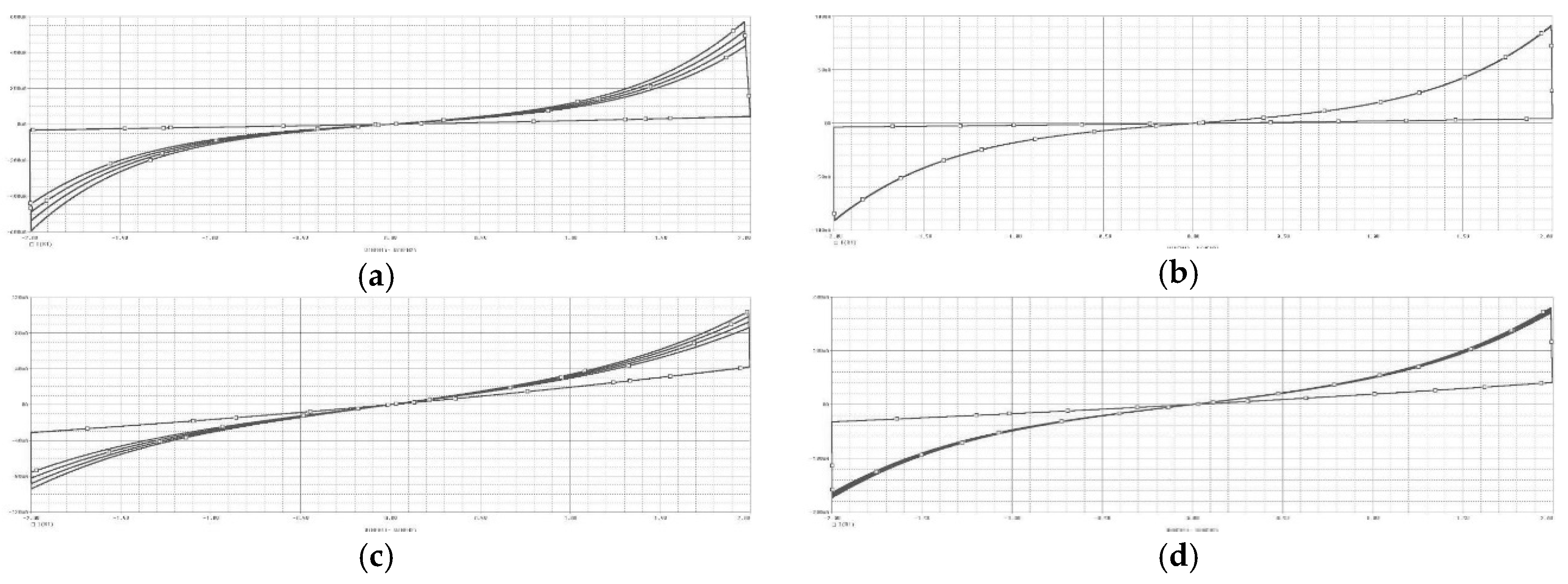
5. PSpice Analysis of a Passive Memristor Memory Matrix

A schematic of a passive memristor memory crossbar is presented in Figure 7 for illustration of its structure and explanation of its operation. Its work procedures are very similar to those described for the hybrid memory matrix presented above.
The corresponding time diagrams of the memristance, state variable, and voltage and the respective i–v relationship of the memristors are presented in Figure 8 for comparison of the results with those derived for the hybrid memory matrix. It can be concluded that in the present case, the sneak parasitic paths do not strongly affect the correct operation of the memory device. A comparison between a single memristor memory element, a 1T1R cell, and a 10T25R memory scheme is made according to several basic parameters and characteristics. The derived results are presented in Table 2 for illustration of the main properties of these memory devices. The single memristor cell has the highest memory window. For a memory crossbar with many memristors, produced in a manufacturing chemical and physical processes, the stability of the parameters and the respective reliability are expected to be higher than these of single memristor prototypes. For a selected memristor cell in the crossbar, the static power is 2.1 µW and the respective dynamic power is 43 µW. The respective power of the MOS transistors connected to the selected memristor is 47 µW. For unselected memristors, the power is 1.2 µW and it is several times lower that the consumed power from the selected memristor element. The corresponding power of the connected MOS transistors is 8.1 µW. Voltage pulses with a level higher than 2 V must be avoided in order to retain the stability and the respective performance of the memory crossbar and to avoid break-through processes and additional Joule heating.
The basic parameters used for the comparison of the applied models (relative root mean square deviation between the i–v relationships ei) [30] are presented in Table 3 for illustration of the advantages of the used memristor models. The analyses are made with a computer system with Intel Processor Core i5, 2.5 GHz, 8 GB RAM. The corresponding simulation times for the applied model with Joglekar, Biolek, modified Joglekar, and modified Biolek windows are, respectively: tJ = 0.8935 s, tB = 0.9127 s, tMJ = 1.0564 s and tMB = 0.9959 s. The models with modified window functions have a little longer simulation times according to the models with the original Joglekar and Biolek windows, due to the increased amount of mathematical operations. Considering the present development of the computer systems and their very high computational power and operating memory, this increased simulation time does not affect the memristor circuits analysis. An advantage of the applied modified Biolek and Joglekar models is the decreased relative root mean squared error with respect to the models with the original Biolek and Joglekar window functions.

6. Conclusions

After analysis of the results derived by the simulations of the applied HfO2 memristor models together with the used modified and original window functions, it can be concluded that the respective current-voltage characteristics have similar behavior during memory operation processes, i.e., writing and reading information. The procedures of writing and reading in a hybrid memory scheme and in a passive memristor matrix were successfully investigated with the used memristor models and the applied modified window functions. A good similarity was found between the simulated and experimental results. It can be concluded that the memristor models used here together with the modified window functions have the capability to represent the behavior of a hafnium-dioxide memristor in memory schemes for general impulse mode and comparatively high-level voltage signals. Unlike several standard linear models, such as Joglekar and Biolek, the applied strongly nonlinear model and window functions successfully modelled the exponential ionic dopant drift for high-level signals and the corresponding switching phenomenon. An advantage of the used model together with the modified Joglekar and Biolek window functions is the established highest proximity between the experimental and the simulated i–v relationships of the memristor. An advantage of the applied models together with the used modified window functions, compared to the Pickett model, is the observed better convergence ability. Another advantage of the applied memristor models is the use of additional highly nonlinear window functions, which enables realistic representation of the nonlinear dopant drift and switching processes according to the memristor state variable.

Author Contributions

Conceptualization, V.M.; methodology, V.M..; software, V.M.; validation, V.M.; formal analysis, V.M.; investigation, V.M.; resources, V.M.; data curation, V.M.; writing—original draft preparation, V.M.; visualization, V.M.

Funding

This research received no external funding.

Conflicts of Interest

The author declares no conflict of interest.

Appendix A

A netlist for PSpice modeling of the modified Biolek model
*Biolek modified model
.subcktmembiolbod a c
R_R4     N04716 0  100
E_DIFF5     N45834 0 VALUE {V(N44965,N45777)}
E_GAIN2     N01744 0 VALUE {15 * V(N01661)}
G_ABMII2     0 N04716 VALUE { V(N02970)        }
R_R10     0 N48430  20
X_S5  N02199 0 N04382 N13325 SCHEMATIC1_S5
E_GAIN6     N53344 0 VALUE {0.15 * V(N00526)}
R_R5     N04607 0  100
G_ABMII3     0 N04607 VALUE { V(N03007)        }
V_CONST2     N02970 0 DC 3
E_MULT1     DER1 0 VALUE {V(N45572)*V(N00907)}
E_GAIN4     N52859 0 VALUE {80e-6 * V(N52754)}
V_CONST3     N03007 0 DC 4
R_R11     0 N48501 20
R_R6     N04530 0 100
E_GAIN7     N53591 0 VALUE {120e-6 * V(N53529)}
G_ABMII4     0 N04530 VALUE { V(N03044)        }
R_R13     N48891 0 1
V_CONST4     N03044 0 DC 5
E_ABM2     N53114 0 VALUE { (exp(V(N53064))-exp(-V(N53064)))/2        }
E_GAIN3     PP 0 VALUE {2 * V(P)}
X_S6   N02199 0 N04305 N13325 SCHEMATIC1_S6
R_R12     0 N48558  20
V_CONST5     N03081 0 DC 6
G_ABMII5     0 N04456 VALUE { V(N03081)        }
E_ABS1     N01545 0 VALUE {ABS(V(N00526))}
R_R7     N04456 0 100
V_CONST6     N03118 0 DC 7
V_CONST10     DER3 0 DC 0
V_CONST7     N03155 0 DC 8
G_ABMII6     0 N04382 VALUE { V(N03118)        }
R_R8     N04382 0 100
G_ABMII8     0 N48430 VALUE { V(DER3)        }
X_S1   N02199 0 N04716 N13325 SCHEMATIC1_S1
E_MULT2     DER2 0 VALUE {V(N45834)*V(N00907)}
E_DIFF6     N50517 0 VALUE {V(N48891,0)}
G_ABMII7     0 N04305 VALUE { V(N03155)        }
E_DIFF3     N44983 0 VALUE {V(X,N44965)}
R_R9     N04305 0 100
G_ABMII9     0 N48501 VALUE { V(DER2)        }
E_SUM1     N01611 0 VALUE {V(N01593)+V(N01545)}
V_CONST8     N44965 0 DC 1.000
V_CONST1     N01593 0 DC 2
X_S2   N02199 0 N04607 N13325 SCHEMATIC1_S2
G_ABMII1     0 N02199 VALUE { V(N01744)        }
G_ABMII10     0 N48558 VALUE { V(DER1)        }
E_PWRS1     N00561 0 VALUE {PWRS(V(N00526),5)}
E_EXP1     N53457 0 VALUE {EXP(V(N53344))}
X_S7   C A N48558 N48891 SCHEMATIC1_S7
E_MULT3     N53213 0 VALUE {V(N53114)*V(N52859)}
R_R1     C 0 1t
E_DIFF2     P 0 VALUE {V(N13325,0)}
E_GAIN1     N00907 0 VALUE {34.5 * V(N00561)}
E_GAIN5     N53064 0 VALUE {1.8 * V(N00526)}
E_PWRS4     N52754 0 VALUE {PWRS(V(X),5)}
X_INTEG1   N50517 X SCHEMATIC1_INTEG1
E_DIFF7     N53529 0 VALUE {V(N53457,N53507)}
E_PWRS3     N45777 0 VALUE {PWRS(V(X),V(pp))}
E_PWRS2     Y 0 VALUE {PWRS(V(N44983),V(pp))}
R_R3     0 N02199 1
R_R2     A C 1t
X_S3   N02199 0 N04530 N13325 SCHEMATIC1_S3
E_ABM1     N01661 0 VALUE { 1/(V(N01611))        }
G_ABMII11     C A VALUE { V(N53666)        }
X_S8   A C N48501 N48891 SCHEMATIC1_S8
E_SUM2     N53666 0 VALUE {V(N53591)+V(N53213)}
R_R16     N13325 0 1
E_DIFF4     N45572 0 VALUE {V(N44965,Y)}
X_S4   N02199 0 N04456 N13325 SCHEMATIC1_S4
E_DIFF1     N00526 0 VALUE {V(A,C)}
X_S9   A C N48430 N48891 SCHEMATIC1_S9
V_CONST9     N53507 0 DC 1.000
.endsmembiolbod

Appendix B

A netlist for PSpice modeling of the modified Joglekar model
*Joglekar modified model
.subcktmemjoglmod a c
*V_V1     A C
*+SIN 0 2.4 1meg 0 0 -5
V_CONST1     N00745 0 DC 1.000
E_DIFF1     U 0 VALUE {V(A,C)}
E_SIN1     N00556 0 VALUE {SIN(V(N00482))}
E_GAIN10     N01741 0 VALUE {0.5 * V(N01671)}
E_GAIN6     N01018 0 VALUE {30e3 * V(N00981)}
E_PWRS1     N00579 0 VALUE {PWRS(V(N00556),2)}
E_EXP1     N01563 0 VALUE {EXP(V(N01470))}
E_DIFF5     N02275 0 VALUE {V(N02194,N00745)}
E_PWRS2     N00820 0 VALUE {PWRS(V(N00763),10)}
E_GAIN9     N01600 0 VALUE {-1 * V(N01470)}
E_MULT2     N01796 0 VALUE {V(N01394)*V(N01741)}
E_PWRS3     N01093 0 VALUE {PWRS(V(U),5)}
E_PWRS4     N01353 0 VALUE {PWRS(V(X),5)}
R_R1     A C  1t
E_EXP2     N01619 0 VALUE {EXP(V(N01600))}
E_GAIN11     N02110 0 VALUE {0.13 * V(U)}
E_DIFF3     FJ 0 VALUE {V(N00745,N00820)}
E_GAIN2     N00620 0 VALUE {2 * V(N00579)}
E_GAIN12     N02334 0 VALUE {15e-6 * V(N02275)}
E_MULT1     N01148 0 VALUE {V(N01093)*V(N01018)}
R_R2     C 0  1t
E_SUM1     N00646 0 VALUE {V(N00926)+V(N00620)}
E_GAIN7     N01394 0 VALUE {9e-6 * V(N01353)}
E_SUM2     I 0 VALUE {V(N02334)+V(N01796)}
E_GAIN3     N00707 0 VALUE {2 * V(X)}
E_GAIN4     N00926 0 VALUE {8 * V(FJ)}
E_DIFF4     N01671 0 VALUE {V(N01563,N01619)}
G_ABMII1     A C VALUE { V(I)        }
X_INTEG1   N01148 X SCHEMATIC1_INTEG1
E_GAIN8     N01470 0 VALUE {1.7 * V(U)}
E_GAIN1     N00482 0 VALUE {3.14 * V(X)}
E_EXP3     N02194 0 VALUE {EXP(V(N02110))}
E_GAIN5     N00981 0 VALUE {0.1 * V(N00646)}
E_DIFF2     N00763 0 VALUE {V(N00707,N00745)}
.endsmemjoglmod

References

  1. Dearnaley, G.; Stoneham, A.; Morgan, D. Electrical phenomena in amorphous oxide films. Rep. Prog. Phys. 1970, 33, 1129–1191. [Google Scholar] [CrossRef]
  2. Oxley, D. Electroforming, Switching and Memory Effects in Oxide Thin Films. Electrocomponent Sci. Technol. 1976, 4, 217–224. [Google Scholar] [CrossRef]
  3. Chua, L. Memristor—The Missing Circuit Element. IEEE Trans. Circuit Theory 1971, 18, 507–519. [Google Scholar] [CrossRef]
  4. Strukov, D.B.; Snider, G.S.; Stewart, D.R.; Williams, R.S. The Missing Memristor Found. Nature 2008, 453, 80–83. [Google Scholar] [CrossRef] [PubMed]
  5. Joglekar, Y.; Wolf, S. The Elusive Memristor: Properties of Basic Electrical Circuits. Eur. J. Phys. 2009, 30, 661–675. [Google Scholar] [CrossRef]
  6. Biolek, D.; Biolkova, V. SPICE Model of Memristor with Nonlinear Dopant Drift. Radioengineering 2009, 18, 210–214. [Google Scholar]
  7. Lupo, N.; Bonizzoni, E.; Pérez, E.; Wenger, C.; Maloberti, F. A Voltage-Time Model for Memristive Devices. IEEE Trans. Very Large Scale Integr. VLSI Syst. 2018, 26, 1452–1460. [Google Scholar] [CrossRef]
  8. Amer, C.; Sayyaparaju, S.; Rose, G.; Beckmann, K.; Cady, N. A practical hafnium-oxide memristor model suitable for circuit design and simulation. In Proceedings of the 2017 IEEE International Symposium on Circuits and Systems (ISCAS), Baltimore, MD, USA, 28–31 May 2017. [Google Scholar]
  9. Corinto, F.; Ascoli, A. A Boundary Condition-Based Approach to the Modeling of Memristor Nanostructures. IEEE Trans. Circuits Syst. Regul. Pap. 2012, 59, 2713–2726. [Google Scholar] [CrossRef]
  10. Ascoli, A.; Tetzlaff, R.; Biolek, Z.; Kolka, Z.; Biolkovà, V.; Biolek, D. The Art of Finding Accurate Memristor Model Solutions. IEEE J. Emerging Sel. Top. Circuits Syst. 2015, 5, 133–142. [Google Scholar] [CrossRef]
  11. Dozortsev, A.; Goldshtein, I.; Kvatinsky, S. Analysis of the row grounding technique in a memristor-based crossbar array. Int. J. Circ. Theor. Appl. 2017, 1–16. [Google Scholar] [CrossRef]
  12. Yang, J.; Zhang, M.; Pickett, M.; Miao, F.; Strachan, J.; Li, W.; Yi, W.; Ohlberg, D.; Choi, B.; Wu, W.; et al. Engineering nonlinearity into memristors for passive crossbar applications. Appl. Phys. Lett. 2012, 100, 1–5. [Google Scholar]
  13. Hamdioui, S.; Xie, L.; Nguyen, H.A.D.; Taouil, M.; Bertels, K.; Corporaal, H.; Jiao, H.; Catthoor, F.; Wouters, D.; Eike, L.; et al. Memristor Based Computation-in-Memory Architecture for Data-Intensive Applications. In Proceedings of the 2015 Design, Automation & Test in Europe Conference & Exhibition (DATE), Grenoble, France, 9–13 March 2015. [Google Scholar]
  14. Raj, S.; Chakraborty, D.; Jha, S.K. In-memory flow-based stochastic computing on memristor crossbars using bit-vector stochastic streams. In Proceedings of the 2017 IEEE 17th International Conference on Nanotechnology (IEEE-NANO), Pittsburgh, PA, USA, 25–28 July 2017. [Google Scholar]
  15. Hamdioui, S.; Taouil, M.; Nguyen, H.A.D.; Haron, A.; Xie, L.; Bertels, K. Memristor: The Enabler of Computation-in-Memory Architecture for Big-Data. In Proceedings of the 2015 International Conference on Memristive Systems (MEMRISYS), Paphos, Cyprus, 8–10 November 2015. [Google Scholar]
  16. Mladenov, V. Analysis and Simulations of Hybrid Memory Scheme Based on Memristors. Electronics 2018, 7, 289. [Google Scholar] [CrossRef]
  17. Abdalla, H.; Pickett, M. SPICE modelling of memristors. In Proceedings of the 2011 IEEE International Symposium of Circuits and Systems (ISCAS), Rio de Janeiro, Brazil, 15–18 May 2011. [Google Scholar]
  18. Linn, E.; Siemon, A.; Waser, R.; Menzel, S. Applicability of Well-Established Memristive Models for Simulations of Resistive Switching Devices. IEEE Trans. Circuits Syst. I Regul. Pap. 2014, 61, 2402–2410. [Google Scholar] [CrossRef]
  19. Kumar, S.; Wang, Z.; Huang, X.; Kumari, N.; Davila, N.; Strachan, J.; Vine, D.; Kilcoyne, A.; Nishi, Y.; Williams, R. Oxygen migration during resistance switching and failure of hafnium oxide memristors. Appl. Phys. Lett. 2017, 110, 103503. [Google Scholar] [CrossRef]
  20. Yang, J.J.; Pickett, M.D.; Li, X.; Ohlberg, D.A.A.; Stewart, D.R.; Williams, R.S. Memristive switching mechanism for metal/oxide/metal nanodevices. Nat. Nanotechnol. 2008, 3, 429–433. [Google Scholar] [CrossRef] [PubMed]
  21. Lehtonen, E.; Laiho, M. CNN using memristors for neighborhood connections. In Proceedings of the 2010 12th InternationalWorkshop on Cellular Nanoscale Networks and their Applications (CNNA 2010), Berkeley, CA, USA, 3–5 February 2010. [Google Scholar]
  22. Ho, Y.; Huang, G.M.; Li, P. Dynamical Properties and Design Analysis for Nonvolatile Memristor Memories. IEEE Trans. Circuits Syst. I Regul. Pap. 2011, 58, 724–736. [Google Scholar] [CrossRef]
  23. Serb, A.; Redman-White, W.; Papavassiliou, C.; Prodromakis, T. Practical determination of individual element resistive states in selectorless RRAM arrays. IEEE Trans. Circuits Syst. I Regul. Pap. 2016, 63, 827–835. [Google Scholar] [CrossRef]
  24. Haron, N.; Hamdioui, S. On Defect Oriented Testing for Hybrid CMOS/Memristor Memory. In Proceedings of the IEEE Asian Test Symposium, New Delhi, India, 20–23 November 2011. [Google Scholar]
  25. Mladenov, V.; Kirilov, S. Advanced Memristor Model with a Modified Biolek Window and a Voltage-Dependent Variable Exponent. IAPGOS 2018, 8, 15–20. [Google Scholar] [CrossRef]
  26. Fleck, K.; la Torre, C.; Aslam, N.; Hoffmann-Eifert, S.; Böttger, V.; Menzel, S. Uniting Gradual and Abrupt SET Processes in Resistive Switching Oxides. Phys. Rev. Appl. 2016, 6, 064015. [Google Scholar] [CrossRef]
  27. Jiang, Z.; Wu, Y.; Yu, S.; Yang, L.; Song, K.; Karim, Z.; Wong, H.-P. A Compact Model for Metal-Oxide Resistive Random Access Memory with Experiment Verification. IEEE Trans. Electron Devices 2016, 63, 1884–1892. [Google Scholar] [CrossRef]
  28. Palm, W. Introduction to MATLAB for Engineers; McGraw-Hill: New York, NY, USA, 2011; ISBN 978-1-259-01205-1. [Google Scholar]
  29. Rashid, M. Introduction to PSpice Using OrCAD for Circuits and Electronics, 3rd ed.; Prentice Hall: Upper Saddle River, NJ, USA, 2004; ISBN 0-13-101988-0. [Google Scholar]
  30. Ascoli, A.; Corinto, F.; Senger, V.; Tetzlaff, R. Memristor model comparison. IEEE Circuits Syst. Mag. 2013, 13, 89–105. [Google Scholar] [CrossRef]
Figure 1. (a) Experimental and simulated current-voltage characteristics of the HfO2 memristor; (b) Time diagrams of the applied voltage and the integer exponent; (c) Window function-state relationships of the used HfO2 memristor models.
Electronics 08 00383 g001
Figure 2. A PSpice schematic of Lehtonen-Laiho model with a modified Biolek window function [25].
Electronics 08 00383 g002
Figure 3. A PSpice schematic of the memristor model (13) with the Joglekar modified window function.
Electronics 08 00383 g003
Figure 4. A fragment of the memristor-based hybrid memory matrix.
Electronics 08 00383 g004
Figure 5. Time diagrams of the memristor voltage, state variable, and memristance for: (a) Biolek modified window function; (b) Joglekar modified window function; (c) Biolek original window function; (d) Joglekar original window function.
Electronics 08 00383 g005
Figure 6. Current-voltage relationships of memristors in the hybrid memory crossbar for: (a) Biolek modified window function; (b) Joglekar modified window function; (c) Biolek original window function; (d) Joglekar original window function.
Electronics 08 00383 g006
Figure 7. A passive 6 × 6 memristor memory crossbar.
Electronics 08 00383 g007
Figure 8. (a) Time diagrams of the memristor voltage, state variable, and memristance, according to the memristor model with a modified Biolek window function; (b) current-voltage relationship of memristors for the passive matrix during the processes of writing and reading information.
Electronics 08 00383 g008
Table 1. Basic parameters and quantities of the applied memristor model.
SymbolElectrical QuantityValue, System International
αV−11.8
βµA90
γV−10.15
χµA150
aVm1
s-5
x0-0.4
bV15
cV2
n-5
p-5
Table 2. Parameters and characteristics of a single memristor memory element, 1T1R and 10T25R.
SymbolParameterValue, SISingle Cell1T1R10T25R
TswSwitching timeµs0.340.360.38
ROFF/RONOFF to ON ratio-258255250
VONON voltageV1.211.251.27
VOFFOFF voltageV0.910.930.95
Pstatic selectedStatic power consumptionµW0.350.452.1
Pstatic un-selectedStatic power consumptionµW0.10.20.4
Pdynamic selectedDynamic consumptionµW111443
Pdynamic un-selectedDynamic powerµW0.70.81.2
Table 3. Parameters for comparison the applied memristor models.
ParameterUnitJoglekar WindowBiolek WindowJoglekar ModifiedBiolek Modified
ei%4.65.44.45.1

