1. Introduction
In high-speed printed circuit boards (PCBs) for digital communication systems, such as USB, HDMI, and PCI-Express technologies, electromagnetic interference during data transmission is a serious problem because the data rate of digital interfaces and the switching speed of processors continuously increase, but the voltage level continuously decreases. In recent high-speed PCB designs, simultaneous switching output noise in power delivery networks and near-field coupling noise in high-speed transmission lines notably undermine digital data transmission. To mitigate the electromagnetic interference effects, differential signaling is usually adopted. Given its balanced transmission, differential signaling is tolerant to both simultaneous switching output noise and near-field coupling noise. Hence, differential signaling is being increasingly adopted in high-speed PCBs by implementing a scheme using three conductor systems, namely positive signal line, negative signal line, and ground plane. Maintaining symmetry of those signal lines over the ground plane in high-speed PCBs is critical, because the noise robustness of differential signaling depends on the balanced scheme. However, it is difficult to prevent asymmetries in practical PCB designs. For instance, the unbalanced structures of meander delay lines, ball–grid–array escape routing, and asymmetric ground via configurations frequently occur during the practical design of high-speed PCBs. Moreover, current-strength mismatch of output driver circuits and trace-length mismatch in cables lead to unbalance in the differential scheme even if the PCB is symmetrical. Consequently, imbalance in differential signaling is inevitable in practical PCBs.
Unbalanced differential lines result in severe common-mode (CM) noise generation in high-speed PCBs [
1,
2,
3,
4]. Specifically, skewed signals in unbalanced differential lines generate wideband CM noise with high-order harmonics in the range of gigahertz and related electromagnetic interference problems. For intra-system electromagnetic interference, CM noise coupled to power delivery networks degrades the noise margin and timing budget of circuits mounted on the same board. Additionally, serious radio-frequency interference is produced when the CM noise flows into cables attached to PCBs. A practical example of radio-frequency interference induced by CM noise is presented in Reference [
5], where experimental results show severe interference between a USB device and a 2.4-GHz wireless LAN device. Hence, CM noise caused by unbalanced differential structures should be mitigated in high-speed PCBs.
To suppress wideband and high-frequency CM noise in high-speed PCBs, metamaterial (MTM)-based techniques were proposed [
6,
7,
8,
9,
10,
11]. In Reference [
6], differential transmission lines (DTLs), using a mushroom-type electromagnetic bandgap (EBG) structure with LTCC process technology, are presented. This type of EBG structure provides a wide stopband for even-mode propagation to suppress CM noise flowing along the differential lines, and the passband characteristics of odd-mode propagation ensure good differential-signal integrity during transmission. Then, CM noise suppression is predicted using dispersion analysis based on a lumped circuit model assuming a periodic structure, but prediction for differential signal transmission is not provided. In Reference [
7], a complementary split ring resonator (CSRR) is employed to suppress CM noise of differential lines in high-speed PCBs. The CSRR etched in a ground plane forms an LC resonator to prevent even-mode propagation and behaves as an LC ladder network for odd-mode propagation. To predict selective CM noise suppression, a dispersion relationship is established from a lumped circuit model. However, the differential transmission characteristics are not estimated before performing full-wave simulations and measurements. As reported in References [
8,
9,
10,
11], a stepped impedance resonator is favorable for MTM-DTLs. In Reference [
8], a stepped impedance resonator is implemented using various sizes for planar patches. A large patch and a narrow branch correspond to low and high characteristic impedances, respectively. CM noise suppression and differential signal quality are examined through full-wave simulations and experiments. In Reference [
9], dual-type transmission lines are proposed to realize an MTM-DTLs. Impedance variations are implemented by alternating microstrip and strip lines, and a dispersion equation based on a periodic condition is derived, but it only predicts CM noise suppression. In References [
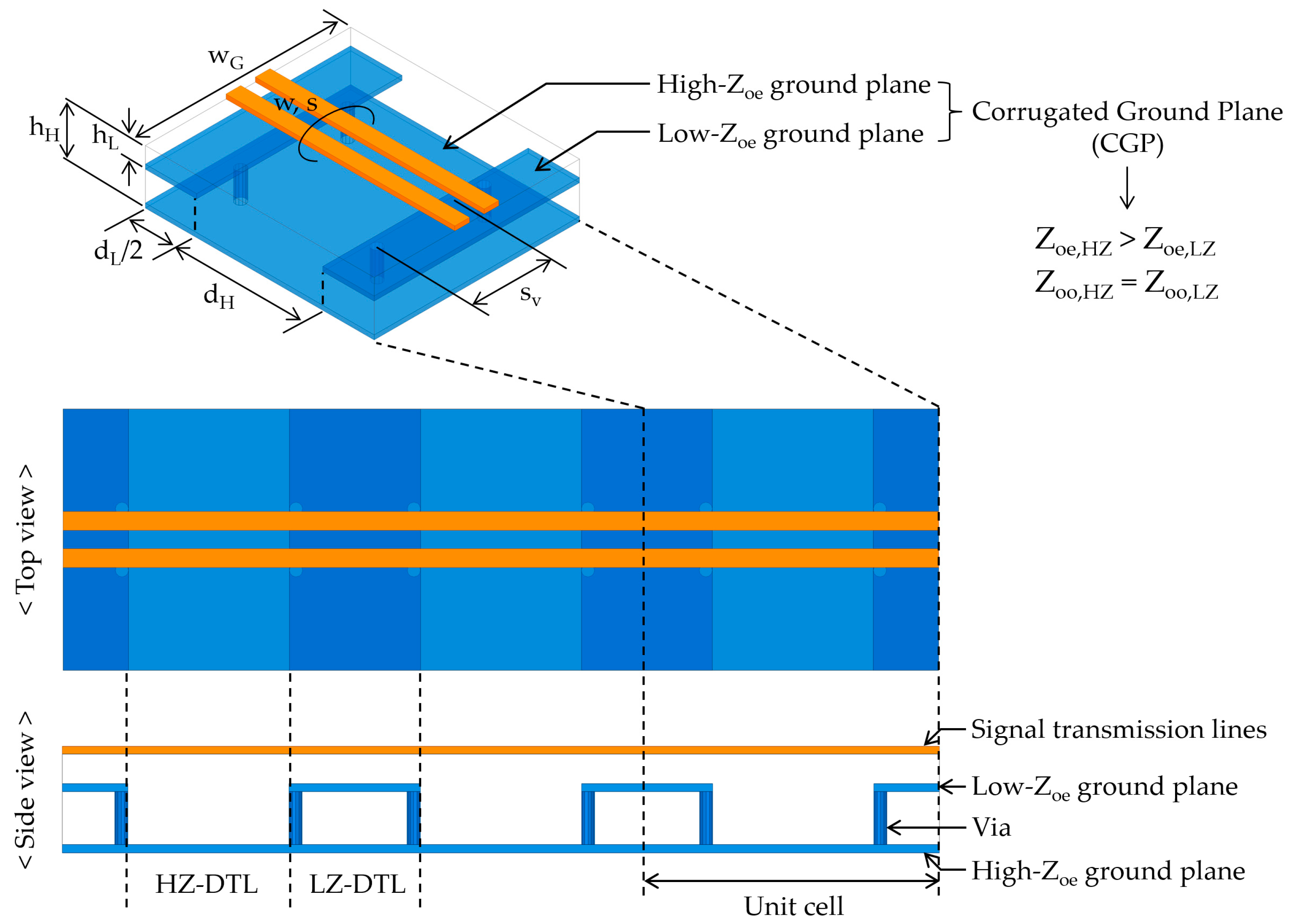
10,
11], a technique with ground planes vertically distributed in PCBs is proposed. The stepped impedance for odd-mode propagation is realized by variations of the vertical distances from differential lines to ground planes, representing a corrugated ground-plane electromagnetic bandgap (CGP-EBG) structure. Dispersion equations for odd-mode propagation are extracted to predict CM noise suppression only.
Therefore, recent research mainly focused on MTM-DTLs for CM noise suppression. It demonstrated wideband and high-frequency CM noise suppression with good differential signal integrity, simple implementation, and rigorous analysis based on dispersion relations. The key idea behind the development of MTM-DTLs is to provide structures handling different characteristics in the propagation modes of CM noise and differential-mode (DM) signal. To efficiently design and optimize MTM-DTLs, predicting and examining CM and DM characteristics of MTM-DTLs before their fabrication is needed. Although electromagnetic full-wave simulations can be employed, their prediction is computationally intensive in time and resources, thus being unsuitable for rapid design, testing, and prototyping of MTM-DTLs.
To overcome this problem, dispersion analysis with Floquet theory was adopted to estimate CM noise suppression. However, this analysis is limited to periodic structures, hindering the estimation of noise suppression characteristics when MTM-DTLs include a finite and small number of unit cells (UCs). Moreover, the periodicity of an MTM-DTL is not ensured in practical PCB applications. Likewise, dispersion analysis does not allow to accurately predict the suppression level, as its results only indicate whether a sufficient suppression will be provided in a stopband without retrieving a quantitative prediction. In addition, CM noise suppression characteristics in regions outside the stopband are not obtained, despite this information being critical in certain MTM-DTL applications. Moreover, the DM propagation associated with differential signaling characteristics was not estimated with a fast and simple approach in previous works. In Reference [
12], the analytical method for the EBG structure employed in power delivery networks is presented. However, it is difficult to apply the method to DTLs because the segment model and recombined Z-parameter are limited to power delivery networks. Consequently, an efficient and accurate method to predict both CM noise and differential signaling characteristics of MTM-DTLs is still required for practical research and development of high-speed PCBs.
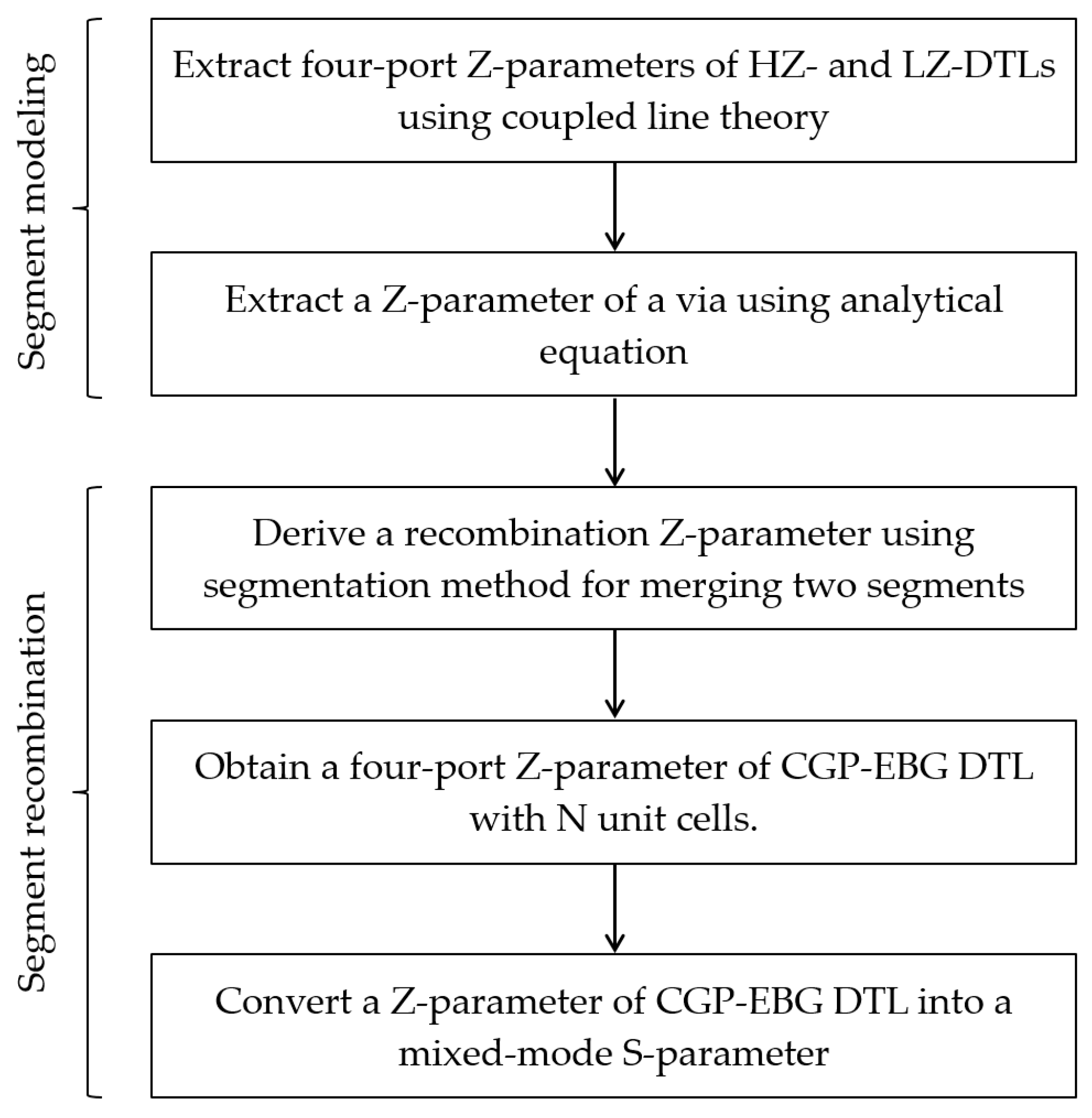
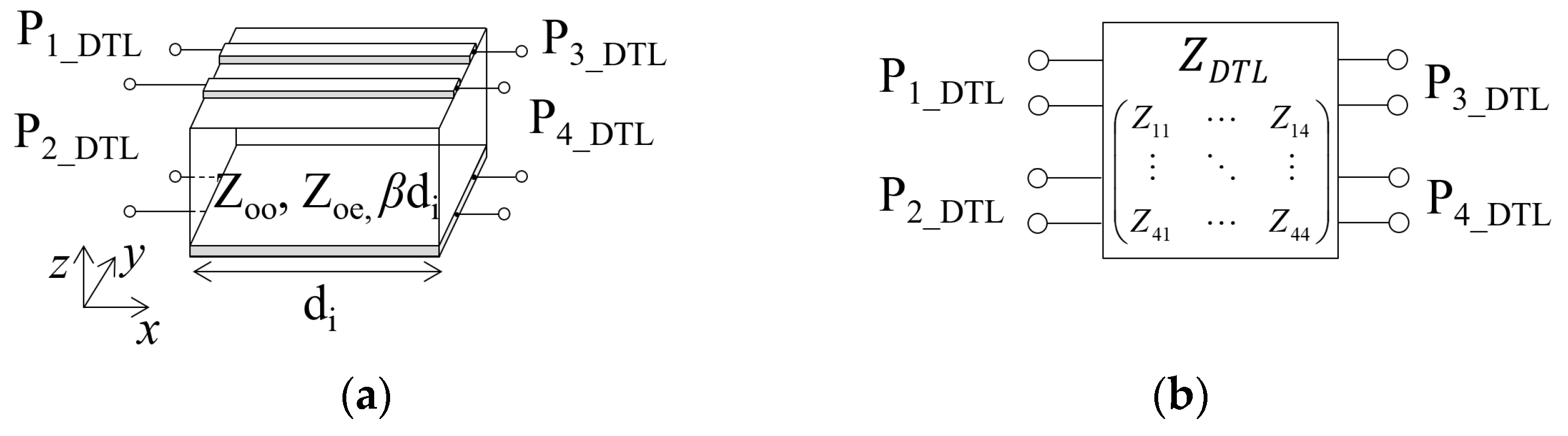
In this paper, an analytical model focusing on the MTM-DTL using a CGP-EBG structure is presented. In previous research [
11], the CGP-EBG MTM-DTL was not fully characterized due to a limited method of CM noise prediction and a lack of estimation of differential transmission characteristics. Therefore, the research of the CGP-EBG MTM-DTL is extended by proposing an analytical model that efficiently provides rapid and accurate results for a nonperiodic array of CGP-EBG MTM-DTLs. The contribution of this paper is developing and verifying the analytical model, which simultaneously and quantitatively estimates the CM and DM propagation characteristics for the CGP-EBG MTM-DTL with a finite number of UCs.
3. Results
To verify the proposed analytical model of CGP-EBG MTM-DTLs, it is compared to full-wave simulations based on the finite element method (FEM) [
18] and measurements. Comprehensive validations were performed considering various cases. Firstly, the CM characteristics of the CGP-EBG MTM-DTLs between the proposed model and full-wave simulations are compared. For the full-wave simulation model, geometrical parameters
dH,
hH,
dL,
hL,
w,
s,
wG, and
sv are set to 10, 1.0, 10, 0.08, 0.1, 0.1, 10, and 1.3 mm, respectively. The values were determined considering a commercial PCB process. FR-4 and copper (35 μm thick) were used as a dielectric material and conductor, respectively. The physical dimensions of the CGP-EBG MTM-DTL present
Zoe,H,
Zoo,H,
Zoe,L, and
Zoo,L of 218, 66.3, 66, and 52 Ω, respectively. The dimensions and parameters for this validation are listed in
Table 1.
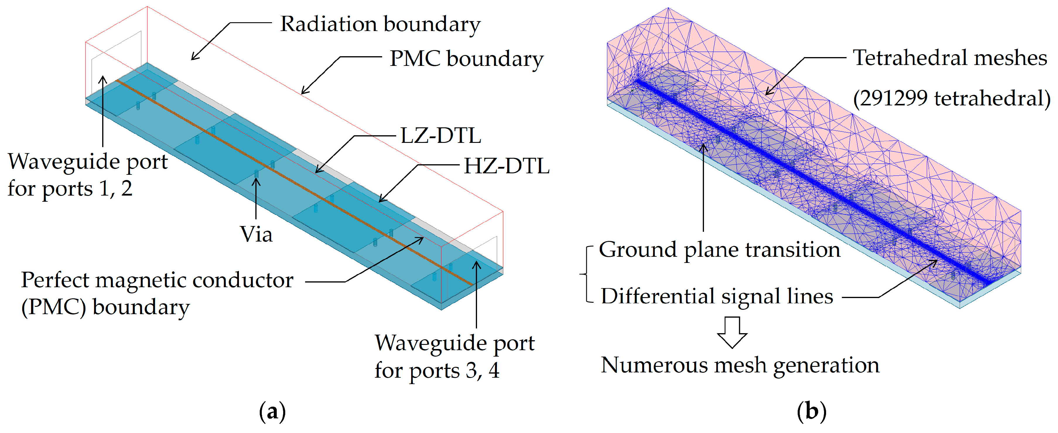
The FEM simulation model for the CGP-EBG MTM-DTLs including three unit cells and their mesh generation result are shown in
Figure 5. The waveguide ports are adopted for the excitation of the CM and DM waves at ports 1, 2, 3, and 4 of the differential signal lines. The perfect magnetic conductor and radiation boundaries are assigned at the sides and top of the vacuum box, which is shown as a red box in the
Figure 5a. The dielectric constant and loss tangent of FR-4 are 4.4 and 0.02, respectively. The via in the FEM model is modeled using a polyhedron with 12 segments. Its radius and height are 0.2 and 0.9 mm, respectively. The meshes are generated with the solution frequency of 10 GHz, which is the maximum frequency of interest. As can be seen in
Figure 5b, most meshes are placed in differential signal lines and ground plane transition.
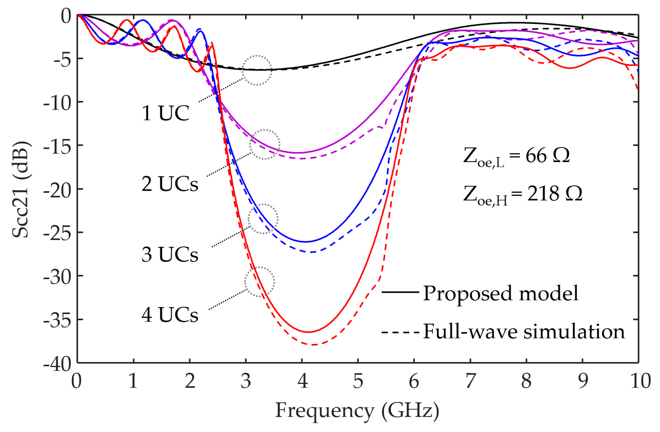
Figure 6 depicts the eight curves of parameter
Scc21 from the CGP-EBG MTM-DTLs considering one to four UCs, using the proposed analytical model (solid lines) and full-wave simulations (dashed lines). The proposed model suitably agrees with the full-wave simulations in the four cases. From the proposed model, the minimum values of CM noise suppression from one to four UCs are −6.1, −15.6, −25.9, and −36.3 dB, respectively. Overall, CM noise suppression improves as the number of UCs increases.
Examining the suppression levels where the suppression bandwidth of 3 GHz is ensured, the values for two to four UCs are −10.1, −14.1, and −18.6 dB, respectively. The value of 3 GHz was selected because it corresponds to the suppression bandwidth predicted by the dispersion analysis based on Floquet theory. The high and low cut-off frequencies from Floquet theory were obtained as 2.7 and 5.7 GHz, respectively. The periodic analysis only estimates the cut-off frequencies, but not the suppression level. As seen in
Figure 6, the suppression level corresponding to Floquet theory notably varies according to the number of UCs. In the practical use of MTM-DTLs for high-speed PCBs, a periodic condition is not commonly ensured, thus requiring the development of approaches such as the proposed model considering MTM DTLs with a finite and small number of UCs.
Remarkably, the proposed analytical model achieves a drastic reduction in computation time compared to the full-wave simulation. For instance, the time for determining
Scc21 of the CGP-EBG MTM-DTL with four UCs using the proposed model was 0.3 s, whereas that using the full-wave simulation was 18,257 s. Hence, the proposed model substantially reduces the computation time while providing a suitable accuracy compared to the full-wave simulation. The time reduction results are listed in
Table 2.
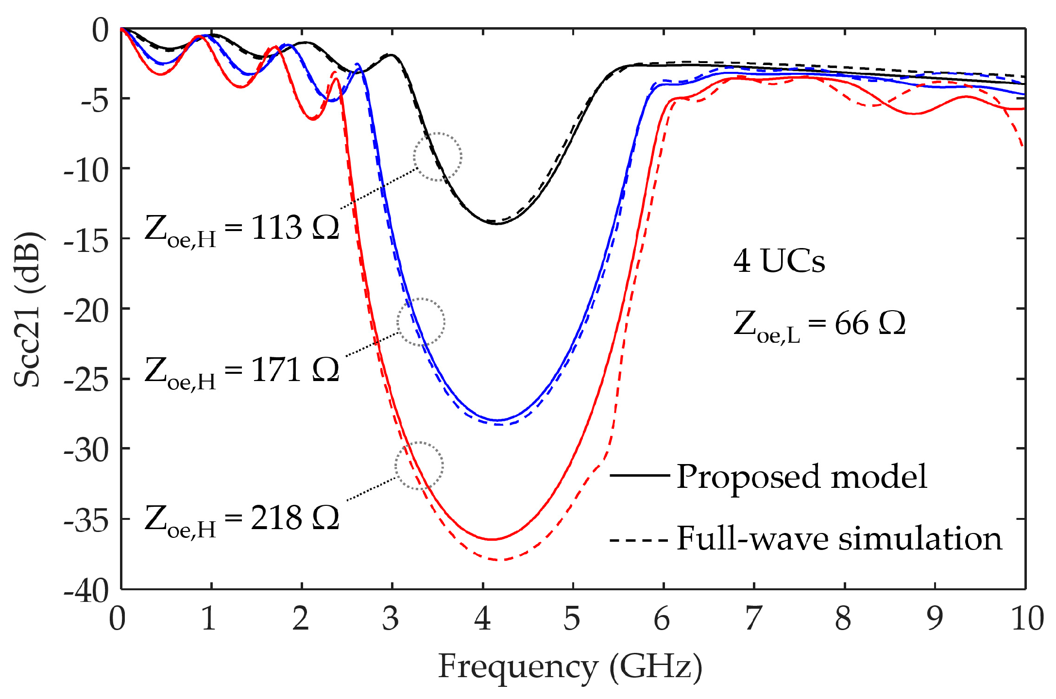
The effect of
Zoe on parameter
Scc21 is further examined by comparing the proposed analytical model and full-wave simulations, as shown in
Figure 7. For the CGP-EBG MTM-DTL with four UCs,
Zoe,H changes to 113, 171, and 218 Ω by adjusting
hH to 0.2, 0.5, and 1.0 mm, respectively. The corresponding changes in the ratio of
Zoe,H to
Zoe,L are approximately 1.7, 2.6, and 3.3. The low and high cut-off frequencies with a suppression level of −10 dB were also investigated. The corresponding (high, low) cut-off frequencies for
Zoe,H of 113, 171, and 218 Ω are (3.56, 4.85 GHz), (2.94, 5.72 GHz), and (2.65, 6.09 GHz), respectively. Hence, the suppression bandwidth and level improve as the ratio of
Zoe,H to
Zoe,L increases. Again, the results of the proposed analytical model are consistent with those of the full-wave simulation.
In addition to CM noise suppression, the differential transmission characteristics of the CGP-EBG MTM-DTLs were investigated.
Figure 8 shows parameter
Sdd21 for differential transmission using the proposed model and full-wave simulations. The design parameters and dimensions are those listed in
Table 1. The values of
Zoo,L and
Zoo,H associated with differential transmission are 52 and 66.3 Ω, respectively. For ideal differential characteristics, the same values of
Zoo between the HZ- and LZ-DTLs are preferred. However, this condition is commonly limited by the design rules of commercial PCB processes, thus making it difficult to avoid different
Zoo values for HZ- and LZ-DTLs in practical high-speed PCBs. The effect of the
Zoo difference on the differential characteristics is shown in
Figure 8. The small difference in the
Zoo values between HZ- and LZ-DTLs degrades differential transmission characteristics. This effect increases with the number of UCs. This phenomenon can be inferred considering the theory of a stepped impedance resonator. However, it is important to obtain the exact degradation of parameter
Sdd21 for measuring and quantitating its impact on differential signal transmission.
The accuracy and efficiency of the proposed analytical model for CGP-EBG MTM-DTLs are verified from comparisons to full-wave simulations based on FEM. The CM noise and differential signal transmission results of the proposed model suitably agree with those of full-wave simulations, but the computation time for obtaining the characteristics of the nonperiodic array of MTM-DTLs was substantially reduced using the proposed four-port analytical model.
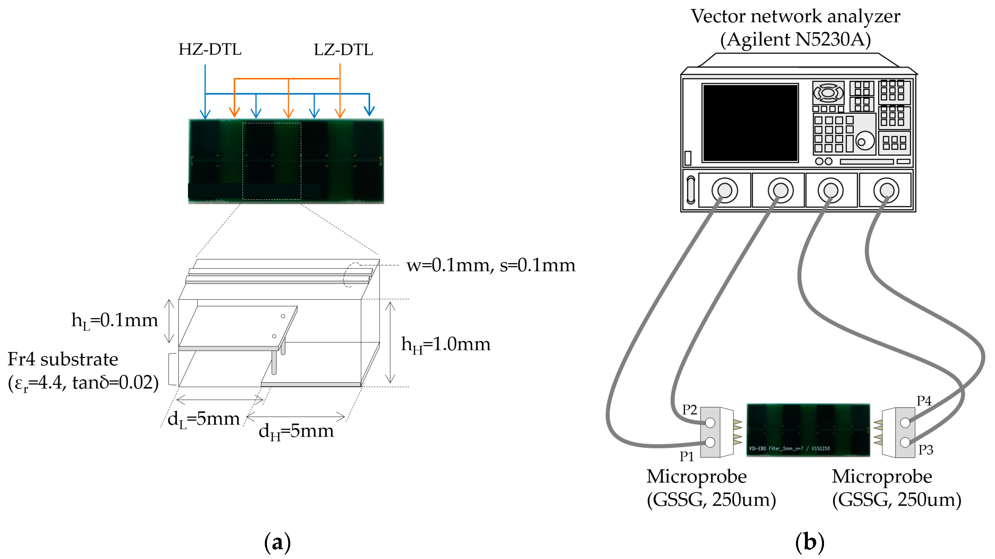
To further validate the proposed model of the CGP-EBG MTM-DTL, the correlations between the proposed model, full-wave simulations, and measurements are examined using the fabricated PCB pattern of the CGP-EBG MTM-DTL. The fabricated PCB pattern and the measurement set-up for S
cc21 and
Sdd21 are shown in
Figure 9. The low-cost PCB process employs the FR-4 dielectric and copper metal layers. The dielectric constant and loss tangent of the FR-4 substrate are 4.4 and 0.02, respectively. The PCB pattern contains four HZ-DTLs and three LZ-DTLs. The geometric dimensions are shown in
Figure 9a. To obtain the
Scc21 and
Sdd21, four-port S-parameters of the PCB pattern are measured using a vector network analyzer and high-frequency microprobes.
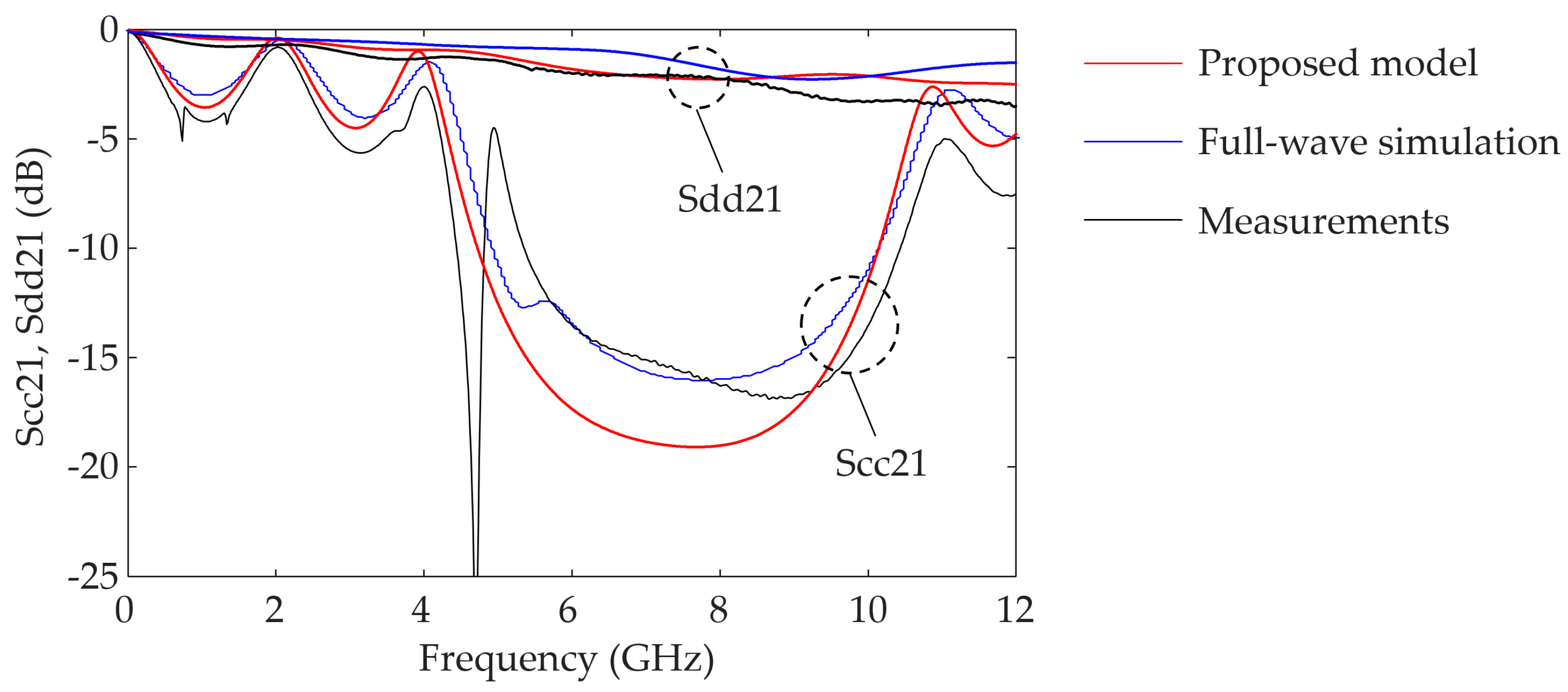
Figure 10 depicts the comparison of
Scc21 and
Sdd21 between the proposed model, full-wave simulations, and measurements. The proposed model agrees well with the measurements. As can be seen in the results, CM noise is successfully suppressed, while good differential data transmission is achieved. In the
Scc21 of the measurements, discrepancy is observed around the frequency of 5 GHz. This defect is caused by PCB manufacturing tolerances because it is not observed in the full-wave simulations.


