Article

Three-Phase Five-Level Cascade Quasi-Switched Boost Inverter

1
Department of Telecommunication Operation, Telecommunications University, Nha Trang 650000, Viet Nam
2
Faculty of Electrical and Electronics Engineering, Ho Chi Minh City University of Technology and Education, 1 Vo Van Ngan Street, Thu Duc District, Ho Chi Minh City 700000, Vietnam
3
Faculty of Electrical and Electronics Engineering, Ho Chi Minh University of Technology (HUTECH), 475A Dien Bien Phu Street, Binh Thanh District, Ho Chi Minh City 700000, Vietnam
4
Department of Electrical Engineering, Chosun University, 309 Pilmun-daero, Dong-gu, Gwangju 61452, Korea
*
Authors to whom correspondence should be addressed.
Electronics 2019, 8(3), 296; https://doi.org/10.3390/electronics8030296
Submission received: 30 January 2019 / Revised: 24 February 2019 / Accepted: 1 March 2019 / Published: 6 March 2019
(This article belongs to the Special Issue Power Converters in Power Electronics)

Abstract

:
This paper presents a three-phase cascaded five-level H-bridge quasi-switched boost inverter (CHB-qSBI). The merits of the CHB-qSBI are as follows: single-stage conversion, shoot-through immunity, buck-boost voltage, and reduced passive components. Furthermore, a PWM control method is applied to the CHB-qSBI topology to improve the modulation index. The voltage stress across power semiconductor devices and the capacitor are significantly lower using improved pulse-width modulation (PWM) control. Additionally, by controlling individual shoot-through duty cycle, the DC-link voltage of each module can achieve the same values. As a result, the imbalance problem of the DC-link voltage can be solved. A detailed analysis and operating principle with the modulation scheme and comprehensive comparison for the CHB-qSBI are illustrated. The experimental and simulation results are presented to validate the operating principle of the three-phase CHB-qSBI.

1. Introduction

Nowadays, multilevel inverters are attractive for high power high voltage applications due to their well-known properties. The benefits of the multilevel power inverter topologies are as follows: improved output waveforms, low electromagnetic interference (EMI), and small filter size [1,2,3]. Neutral point clamped (NPC), flying capacitors, and cascaded H-bridge (CHB) inverters [4,5,6,7,8,9,10,11,12,13,14] are three basic multilevel inverter structures. Among these structures, the CHB structures [9,10,11,12,13,14] have unique merits: higher output voltage, flexibility, and power levels. Furthermore, the CHB inverter can achieve high reliability with modular configuration. The output voltage of each phase in the CHB inverter is achieved by the sum of each output voltage. The CHB structure has some merits in using cascading more H-bridge modules and independent sources. Besides that, the output voltage of the CHB inverter has a high number of levels and reaches medium voltage which results in removing the boost transformer and dropping the size of the output filter. In [14], the low-frequency transformers were used to cascade the H-bridge circuit with a single DC source, but the size of the cascaded system is increased because of using low-frequency transformers.
However, the traditional CHB inverter [9,10,11,12,13,14] is a buck DC–AC power conversion. In addition, both power switches in the same branch cannot be turned on at the same time. To overcome the limitation of the traditional CHB inverters, the CHB quasi-Z-source inverters (CHB-qZSI) were discussed in [15,16,17]. A battery-energy-stored CHB-qZSI-based photovoltaic power generation system was presented in [18]. To enhance the performance of the three-phase five-level CHB-qZSI for grid-connected applications, an innovative modulation technique was introduced in [19] for the voltage stress reduction. A fault-tolerant strategy for the three-phase CHB-qZSI was presented in [20]. In the CHB-qZSI, each module of the three-phase CHB-qZSI topology uses two inductors and two capacitors. As a result, the size, weight, and cost of the cascaded system are increased significantly when the number of output voltage levels is increased. The quasi-switched boost inverter (qSBI) topology had been introduced in [21] to replace the qZSI because it has the same feature as buck-boost voltage and high reliability with shoot-through (ST) immunity. A detailed comparison between qZSI and qSBI topology was discussed in [22]. The comparison results in [22] show that the qSBI topology uses one less capacitor and one less inductor; higher boost factor with the same parasitic effect; lower current rating on switches and diodes; and higher efficiency when compared to qZSI topology. However, with a simple boost control method, the modulation index is low when a voltage gain is required. To improve the modulation index, a novel pulse-width modulation (PWM) scheme for qSBI was proposed in [23]. The single-phase grid-connected CHB-qSBI was discussed in [24]. In CHB-qSBI [24], each module of the CHB-qSBI topology only uses one inductor and one capacitor. A three-phase CHB-qSBI has been proposed in [25] with only some simulation results. Besides that, with using a simple boost method, the CHB-qSBI in [24,25] must use a small modulation index to be able to achieve a high voltage gain. Consequently, the voltage stress across power semiconductor devices and capacitor is high.
To explore more features of the three-phase CHB-qSBI, this paper presents the operating theories, circuit analysis, and experimental verification of the three-phase CHB-qSBI in detail. Furthermore, a PWM control method in [23] is applied to the CHB-qSBI topology to improve the modulation index. The stress voltage across power semiconductor devices and the capacitor is significantly dropped in comparison to CHB-qSBI with using conventional PWM control. To solve the imbalance problem of the DC-link voltage, ST duty cycle of each module is controlled individually. As a result, the DC-link voltage of each module can obtain the same values. The simulation and experimental results are provided to validate the operating principle of the three-phase CHB-qSBI under improved PWM method.

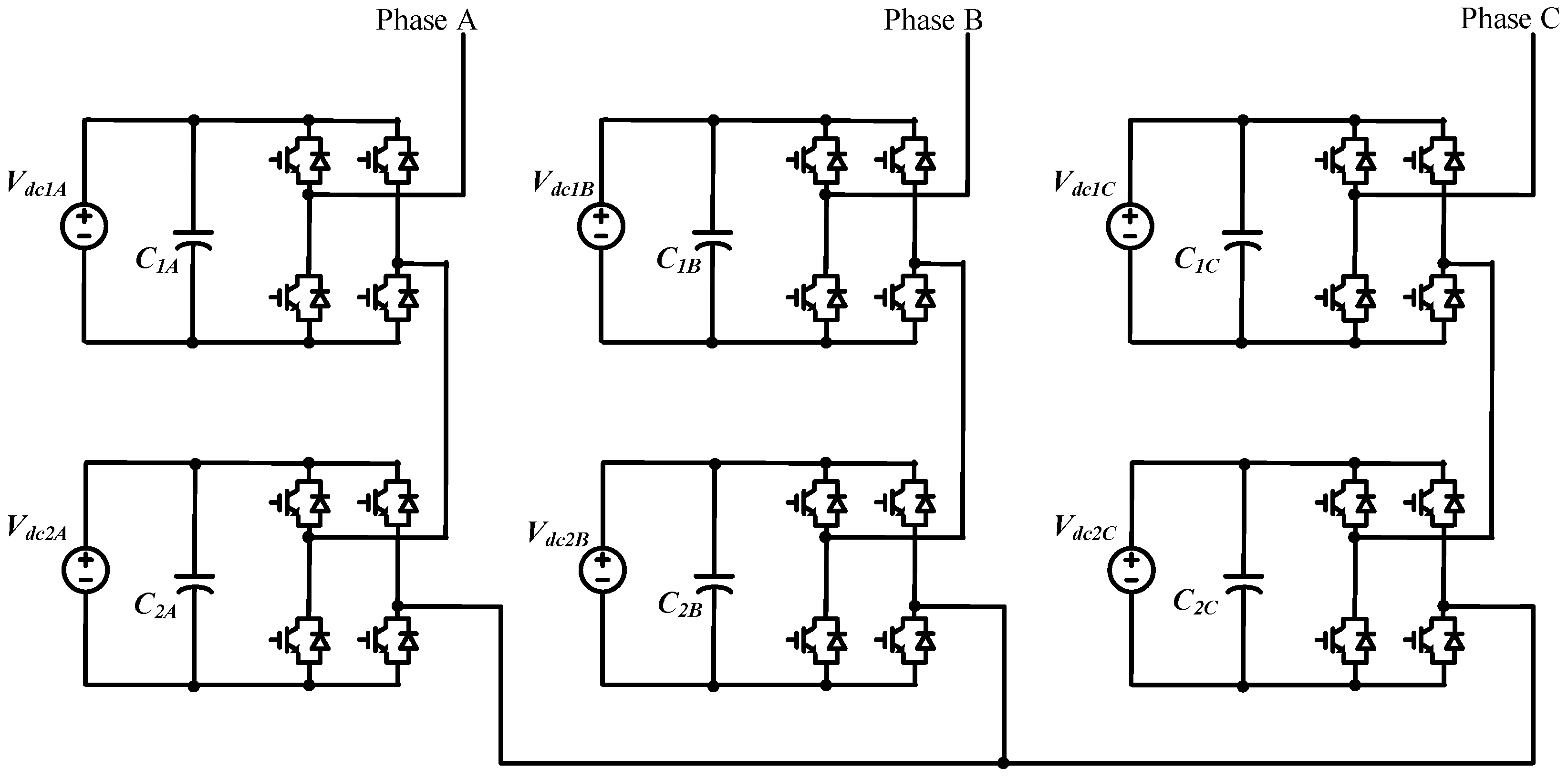
2. Conventional Three-Phase CHB Inverter Topologies

Figure 1 illustrates the traditional three-phase five-level CHB inverter. Two H-bridge circuits were used in each phase to generate a five-level output voltage. Each H-bridge module was connected to the isolated DC voltage source. In the conventional CHB inverter, both upper and lower switches of the H-bridge leg cannot be switched on at the same time. The dead-time between upper and lower switches should be employed to avoid the ST phenomenon in the H-bridge circuit.
Figure 2 presents the three-phase CHB-qZSI topology, where each quasi-Z-source network module used two pair of inductor and capacitor. By adding the ST time interval to the H-bridge switches, the DC-link voltage of each H-bridge module in the CHB-qZSI was boosted to a higher value than the DC source voltage. The CHB-qZSI has the buck-boost voltage function, single-stage conversion, and ST immunity.

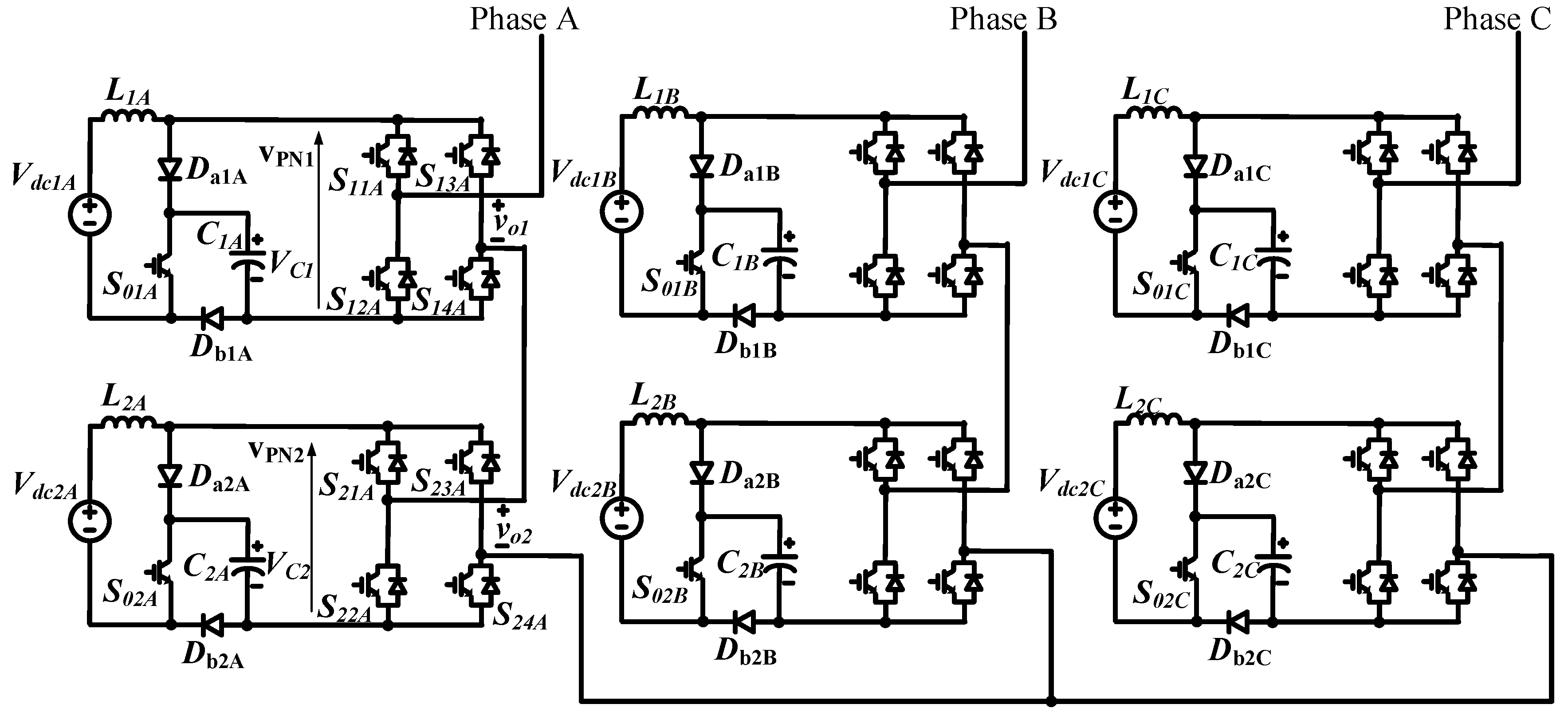
3. Three-Phase CHB-qSBI

The three-phase CHB-qSBI topology is indicated in Figure 3. Similar to conventional CHB inverter topology, each phase of the CHB-qSBI consists of two qSBI modules. The proposed cascaded system consists of six qSBI modules, three filter inductors, six separate DC sources, and a three-phase load. Compared to the conventional CHB module, a qSBI module includes one capacitor, one inductor, two diodes, and one active switch is added.

3.1. Operating Principle

As an example, the module 1 in the introduced system is used to analyze the circuit. As shown in Figure 4, there were three operating states: the non-shoot-through (NST) 1 state, the NST 2 state, and the shoot-through (ST) state.
In NST 1 state as shown in Figure 4a, switch S0 is switched on. During this state, diode Da1 conducts while diode Db1 is blocked. As a result, the capacitor is discharged while the inductor stores energy. The time interval in this state is (0.5 − D1/2).T, where D1 is the duty cycle of each cycle of module 1; T is a switching period. We obtain:
{ L 1 d i L 1 d t = V d c 1 C 1 d v C 1 d t = I P N 1 ,
where IPN1 is the equivalent DC-link current at load side.
In ST state as shown in Figure 4b, both 4 switches on the H-bridge circuit and switch S0 are switched on at the same time. During this state, two diodes Da1 and Db1 are blocked. As a result, the capacitor is discharged, while the inductor stores energy. The time interval in this state is D1.T. We obtain:
{ L 1 d i L 1 d t = V d c 1 + V c 1 C 1 d v C 1 d t = I i n ,
where Iin is the average value of the input current (inductor current).
In NST 2 state as shown in Figure 4c, switch S0 is switched off and the inverter has two active states and two zero states of the inverter main circuit for single-phase topology. During the NST state, Da1 and Db1 are turned on. As a result, the capacitor is charged from Vdc1, while the inductor transfers energy from the DC voltage source to the main circuit. The time interval in this state is (0.5 − D1/2).T. We obtain:
{ L 1 d i L 1 d t = V d c 1 V c 1 C 1 d v C 1 d t = I i n I P N 1 .
Applying the volt-second balance and ampere-second balance principles to L and C in steady state, Equations (1), (2), and (3) yield:
{ V c 1 = 2 1 3 D 1 V d c 1 I i n = 2 ( 1 D 1 ) 1 3 D 1 I P N 1 .
The peak value of DC-link voltage that crosses the inverter of module 1 can be expressed in the NST states as:
V P N 1 = V c 1 = 2 1 3 D 1 V d c 1

3.2. Improved PWM Control for Three-Phase CHB-qSBI

A PWM technique for the single-phase qSBI to improve modulation index was presented in [23]. In this section, the PWM technique in [23] will be extended to the three-phase CHB-qSBI. The PWM strategy for the cascaded system for phase A with the modulation in Figure 4 is illustrated in Figure 5. For module 1, a fixed voltage VSH1 was compared to the triangle waveform (dashed line) with double frequency and half of the amplitude of that of Vtri to generate the ST state in the inverter bridge. Besides that, a square pulse signal with the same frequency as the triangle waveform (dashed line) and 50% duty cycle was used to control the S0 switch. Two control waveforms, Vcontrol and −Vcontrol, were compared to a triangle waveform, Vtri, to generate control signals for H-bridge switches. The additional switch S0 signal was produced by comparing between the saw-tooth waveform, vsaw and VSH1. Table 1 describes a truth table of the switching states of the switches in module 1. The switching status 0 and 1 in Table 1 represents the turning off and turning on of the switches, respectively.
The output voltage vo1 of H-bridge module 1 has three levels: −VPN1, 0, and VPN1. For module 2, the high-frequency triangle waveform, Vtri, was shifted in 90° and the high-frequency triangle waveform *vtri was shifted in 180° to generate the output voltage vo2 of H-bridge module 2. The output voltage of the cascaded system is total vo1 and vo2. As a result, the 5-level output voltage of the proposed cascaded system was produced.

4. Comparison between Three-Phase CHB-qSBI under Improved PWM Method and Three-Phase CHB-qZSI

Table 2 compares the passive components, semiconductor devices, and the governing equations of the three-phase CHB-qSBI and the three-phase CHB-qZSI. From Table 2, the three-phase five-level CHB-qSBI uses six fewer capacitors, six fewer inductors, six more switches, and six more diodes. Although the three-phase CHB-qSBI reduces the number of passive components, it increases the number of active components. The three-phase CHB-qSBI under the improved PWM method uses a higher modulation index to produce the same voltage gain. Figure 6 compares the voltage stresses on diodes and switches of the CHB-qZSI and CHB-qSBI for the same voltage gain. As shown in Figure 6, the voltage stresses of the CHB-qSBI is lower than those of the CHB-qZSI. Consequently, the stress voltage across power semiconductor devices and the capacitor of the three-phase CHB-qSBI was significantly lower. Therefore, the weight, cost, and size of the three-phase CHB-qSBI under the improved PWM method were reduced in comparison with the three-phase CHB-qZSI topology.

5. Simulation and Experimental Verifications

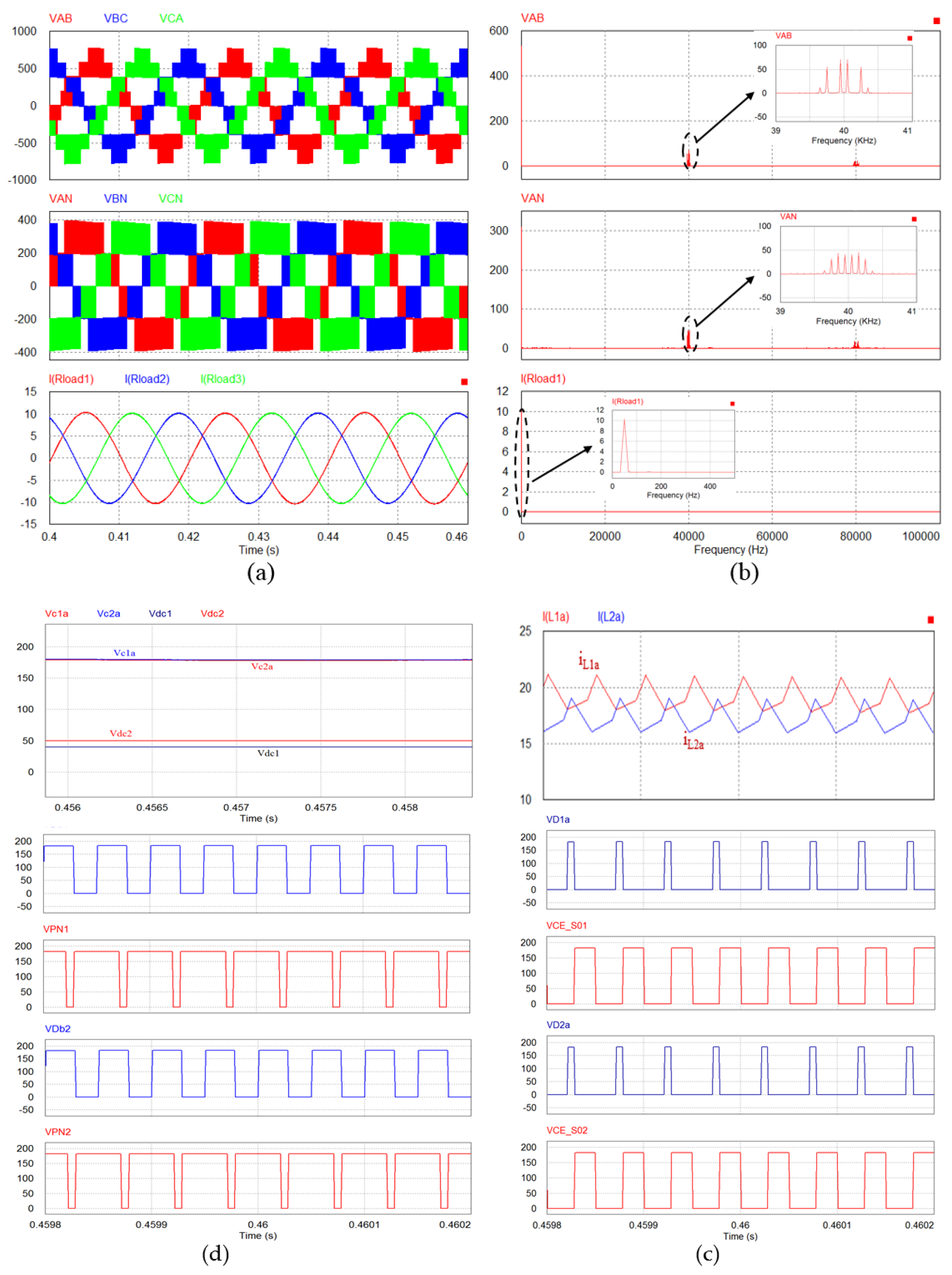
5.1. Simulation Verification

To confirm the theoretical discussion of the three-phase CHB-qSBI in this paper, the software for power electronic named PSIM 9.1 was used to simulate the suggested inverter. The major parameters of the simulation are as follow: the output phase voltage is 220 Vrms with five-level; the AC side filter and load are 10 mH and 30 Ω, respectively; the inductor-capacitor and switching frequency for each module are 1 mH, 2200 µF, and 10 kHz. The list of parameters in the simulation is provided in Table 3. It is worth noting that the high valued DC electrolytic capacitors of 2200 µF were used in the simulation and experiment because the double-line-frequency ripple is not suppressed in the CHB-qSBI system. As analyzed in [16,22,26], the single-phase qSBI had a double-line-frequency ripple on the passive element at the DC side. The double-line-frequency ripple caused several problems related to efficiency, lifetime, cost, size, and reliability of the inverter system. To suppress the double-line-frequency ripple on quasi-switched boost network, a feedback controller for qSBI was introduced in [27].
The simulation results for the three-phase CHB-qSBI are noted in Figure 7 and Figure 8. In Figure 7, the input voltages of Vdc1 and Vdc2 were set the same value of 50 V. It is clear that both the capacitor voltages in all quasi-switched-boost networks were boosted to 195 V. The DC-link voltages were the square waveform and the peak DC-link voltages were equal to the capacitor voltages, as shown in Figure 7c. The DC-link voltage of two quasi-switched-boost modules was the same with the same ST duty cycle. The root mean square (RMS) value output voltage for each phase was 220 V. The peak output current in each phase was 10.3 A. The total harmonic distortion (THD) of the output phase current was 1.6%. Figure 7e shows the simulation results at the start-up process. The inrush currents have appeared in the inductors at the start-up owing to the existing passive elements in the quasi-switched-boost network. It can be seen in Figure 7a that the proposed three-phase CHB-qSBI operated in a stable state after 0.15 s. Figure 7e shows the simulation results when the load was changed from 30 Ω to 60 Ω at 0.4 s.
Next, the suggested inverter was tested with the unbalanced condition of the input voltage. The input voltage Vdc1 was 40 V, while Vdc2 was 50 V. In Figure 8, the simulation results for unbalanced input voltage have been shown. The capacitor voltage and the DC-link voltage are slightly different between the two quasi-switched-boost modules; this is a small insignificant difference in the steady state. Clearly, both of the capacitor voltages in all quasi-switched-boost parts were also boosted to 195 V. The DC-link voltages were the square waveform and the peak DC-link voltages were equal to the capacitor voltages, as shown in Figure 8c. The DC-link voltage of two quasi-switched-boost modules was the same with the same ST duty cycle. The RMS value of the output voltage for each phase was 220 V. The peak output current in each phase was 10.3 A. The THD of the output phase current was 1.7%. The suggested inverter can improve the unbalanced problems in comparison with the conventional CHB inverter.

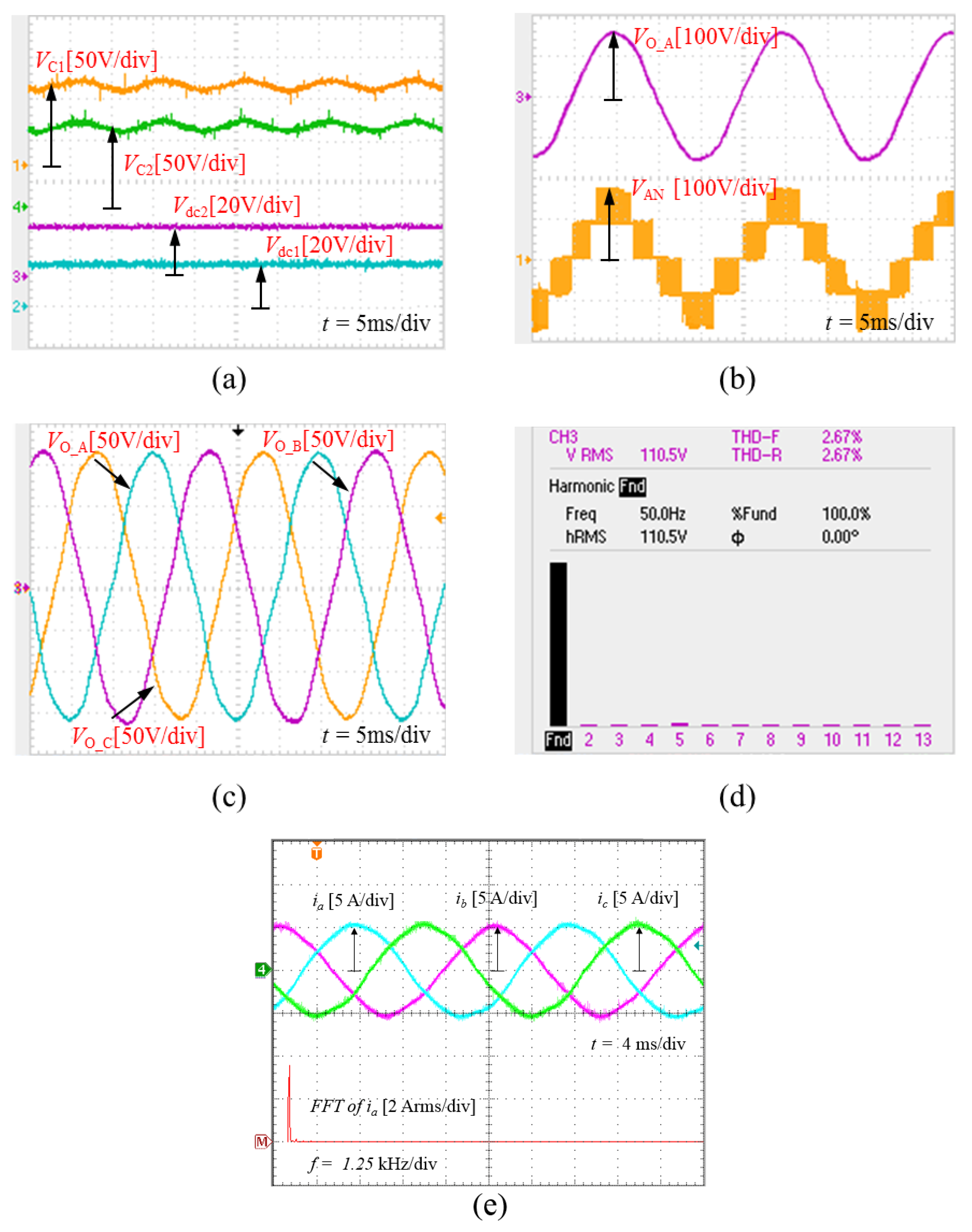
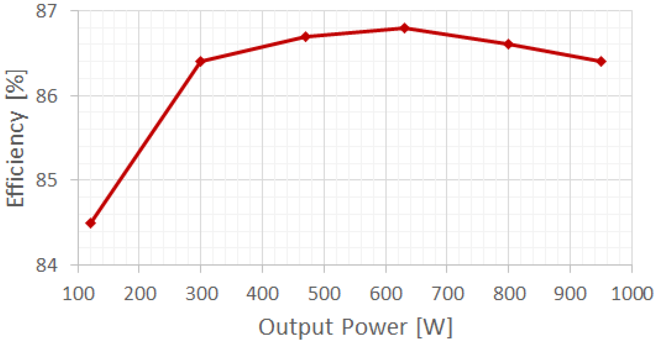
5.2. Experimental Verifications

A scaled-down laboratory prototype of the three-phase CHB-qSBI inverter was built as shown in Figure 9. The microcontroller was DSP TMS320F28335. All switches were G40N120 IGBTs. The diodes were DSEI60-06A. The inductors, capacitors, and load parameters in the experiment were the same as the simulation. The switching frequency was 10 kHz. The RMS value of the output voltage for each phase was 110 V.
The experimental results were tested with the unbalanced input voltage condition. The input voltages Vdc1 and Vdc2 were 20 V and 25 V, respectively. The capacitor voltage and DC-link voltage were boosted to the same value of 92 V for all modules, shown in Figure 10a. The DC-link voltage of the two modules was kept on the same value by controlling the ST duty cycle even though the input voltage of the two modules was different. The output phase voltage, VAN, had five levels: −180 V, −90 V, 0, 90 V, and 180 V, as shown in Figure 10b. The maximum output voltage had a lower value than the total voltage of DC-link voltages because of the voltage drop in the H-bridge circuit. The measured output phase voltage after the filter was 110.5 Vrms. The measured output current was 3.68 Arms, as shown in Figure 10e. The three-phase output voltage and harmonic spectrum of phase-A voltage are seen in Figure 10c,d. The THD of output voltage after the filter was 2.67%. The experimental results were consistent with the simulation.
The efficiency of the proposed inverter was measured at the unbalanced condition input voltage, Vdc1 = 20 V and Vdc2 = 25 V, as shown in Figure 11. The maximum efficiency of the inverter was 86.8% at the output power of 630 W. The efficiency of the inverter was not high because the selection of semiconductor devices in the experiment was not optimal.

6. Conclusions

The configuration three-phase CHB-qSBI is presented in this paper. The three-phase CHB-qSBI can buck-boost voltage with single-stage power conversion. Furthermore, the three-phase CHB-qSBI immunized the ST phenomenon. In comparison to the three-phase CHB-qZSI, the CHB-qSBI dropped a large number of inductors and capacitors. The DC-link voltage of each module can achieve the same values by controlling the ST duty cycle. The paper describes the circuit analysis, operating theories, and PWM strategy of the introduced topology. Simulation and experimental results prove the validity of the improved PWM strategy for controlling the three-phase CHB-qSBI. The three-phase CHB-qSBI can be applicable.

Author Contributions

All authors contributed equally to this work and all authors have read and approved the final manuscript.

Funding

This research was funded by the Korea Institute of Energy Technology Evaluation and Planning (KETEP), and the Ministry of Trade, Industry and Energy (MOTIE) of the Republic of Korea grant number 20184010201650 and the APC was funded by KETEP and MOTIE.

Acknowledgments

This work was supported by the Korea Institute of Energy Technology Evaluation and Planning (KETEP) and the Ministry of Trade, Industry and Energy (MOTIE) of the Republic of Korea (NO. 20184010201650).

Conflicts of Interest

The authors declare no conflict of interest.

Abbreviations

CHBCascaded H-bridge
D1Shoot-through duty cycle
DSPDigital signal processing
EMIElectromagnetic interference
FCFlying capacitor
NPCNeutral point clamped
NSTNon-shoot-through
PWMPulse-width modulation
qSBIquasi-switched boost inverter
STShoot-through
TPeriod time
qZSIQuasi-Z-source inverter

References

  1. Malinowski, M.; Gopakumar, K.; Rodriguez, J.; Pérez, M.A. A survey on cascaded multilevel inverters. IEEE Trans. Ind. Electron. 2010, 57, 2197–2206. [Google Scholar] [CrossRef]
  2. Su, G.J. Multilevel dc-link inverter. IEEE Trans. Ind. Appl. 2005, 41, 848–854. [Google Scholar] [CrossRef]
  3. Calais, M.; Borle, L.J.; Agelidis, V.G. Analysis of multicarrier PWM methods for a single-phase five-level inverter. In Proceedings of the 2001 IEEE 32nd Annual Power Electronics Specialists Conference, Vancouver, BC, Canada, 17–21 June 2001; Volume 3, pp. 1173–1178. [Google Scholar]
  4. Pou, J.; Pindado, R.; Boroyevich, D. Voltage-balance limits in four-level diode-clamped converters with passive front ends. IEEE Trans. Ind. Electron. 2005, 52, 190–196. [Google Scholar] [CrossRef]
  5. Hammami, M.; Rizzoli, G.; Mandrioli, R.; Grandi, G. Capacitors voltage switching ripple in three-phase three-level neutral point clamped inverters with self-balancing carrier-based modulation. Energies 2018, 11, 3244. [Google Scholar] [CrossRef]
  6. Son, Y.; Kim, J. A novel phase current reconstruction method for a three-level neutral point clamped inverter (NPCI) with a neutral shunt resistor. Energies 2018, 11, 2616. [Google Scholar] [CrossRef]
  7. Meynard, T.A.; Foch, H.; Thomas, P.; Courault, J.; Jakob, R.; Nahrstaedt, M. Multilevel converters: Basic concepts and industry applications. IEEE Trans. Ind. Electron. 2002, 49, 955–964. [Google Scholar] [CrossRef]
  8. Kang, K.P.; Cho, Y.; Kim, H.S.; Baek, J.W. DC-link capacitor voltage imbalance compensation method based injecting harmonic voltage for cascaded multi-module neutral point clamped inverter. Electronics 2019, 8, 155. [Google Scholar] [CrossRef]
  9. Kang, J.W.; Hyun, S.W.; Ha, J.O.; Won, C.Y. Improved neutral-point voltage-shifting strategy for power balancing in cascaded NPC/H-bridge inverter. Electronics 2018, 7, 167. [Google Scholar] [CrossRef]
  10. Noman, A.M.; Al-Shamma’a, A.A.; Addoweesh, K.E.; Alabduljabbar, A.A.; Alolah, A.I. cascaded multilevel inverter topology based on cascaded H-bridge multilevel inverter. Energies 2018, 11, 895. [Google Scholar] [CrossRef]
  11. Villanueva, E.; Correa, P.; Rodriguez, J.; Pacas, M. Control of a single-phase cascader H-bridge multilevel converter for grid-connected photovoltaic systems. IEEE Trans. Ind. Electron. 2009, 56, 4399–4406. [Google Scholar] [CrossRef]
  12. Kouro, S.; Moya, A.; Villanueva, E.; Correa, P.; Wu, B.; Rodriguez, J. Control of a cascaded H-bridge converter for grid-connected photovoltaic systems. In Proceedings of the IEEE 35th Annual Conference of the Industrial Electronics Society, Porto, Portugal, 3–5 November 2009; Volume 9, pp. 1–7. [Google Scholar]
  13. Viola, F. Experimental evaluation of the performance of a three-phase five-level cascaded H-bridge inverter by means FPGA-based control board for grid connected applications. Energies 2018, 11, 3298. [Google Scholar] [CrossRef]
  14. Suresh, Y.; Pand, A.K. Research on a cascaded multilevel inverter by employing three-phase transformers. IET Power Electron. 2012, 5, 561–570. [Google Scholar] [CrossRef]
  15. Zhou, Y.; Liu, L.; Li, H. A high-performance photovoltaic module-integrated converter (MIC) based on cascaded quasi-Z-source inverters (qZSI) using eGaN FETs. IEEE Trans. Power Electron. 2013, 28, 2727–2738. [Google Scholar] [CrossRef]
  16. Sun, D.; Ge, B.; Yan, X.; Bi, D.; Zhang, L.H.Y.; Abu, H.; Ben, L.; Feng, F.Z. Modeling, impedance-design, and efficiency analysis of quasi-Z source module in cascaded multilevel photovoltaic power system. IEEE Trans. Ind. Electron. 2014, 61, 6108–6117. [Google Scholar] [CrossRef]
  17. Sun, D.; Ge, B.; Peng, F.Z.; Haitham, A.R.; Bi, D.; Liu, Y. A new grid-connected PV system based on cascaded H-bridge quasi-Z source inverter. In Proceedings of the IEEE International Symposium on Industrial Electronics (ISIE), Hangzhou, China, 28–31 May 2012; pp. 951–956. [Google Scholar]
  18. Ge, B.; Liu, Y.; Abu-Rub, H.; Peng, F.Z. State-of-charge balancing control for a battery-energy-stored quasi-Z-source cascaded-multilevel-inverter-based photovoltaic power system. IEEE Trans. Ind. Electron. 2018, 65, 2268–2279. [Google Scholar] [CrossRef]
  19. Miceli, R.; Schettino, G.; Viola, F. Performance evaluation of a three-phase five-level quasi-Z-source cascaded h-bridge for grid-connected applications. In Proceedings of the IEEE International Power Electronics and Application Conference and Exposition (PEAC), Shenzhen, China, 4–7 November 2018; pp. 1–6. [Google Scholar]
  20. Aleenejad, M.; Mahmoudi, H.; Moamaei, P.; Ahmadi, R. A fault-tolerant strategy based on fundamental phase shift compensation for three phase multilevel converters with quasi-Z-Source networks. In Proceedings of the IEEE Power and Energy Conference at Illinois (PECI), Urbana, IL, USA, 19–20 February 2016; pp. 1–6. [Google Scholar]
  21. Nguyen, M.K.; Le, T.V.; Park, S.J.; Lim, Y.C. A class of quasi-switched boost inverters. IEEE Trans. Ind. Electron. 2015, 62, 1526–1536. [Google Scholar] [CrossRef]
  22. Nguyen, M.K.; Lim, Y.C.; Park, S.J. A comparison between single-phase quasi-Z-source and quasi-switched boost inverters. IEEE Trans. Ind. Electron. 2015, 62, 6336–6344. [Google Scholar] [CrossRef]
  23. Nguyen, M.K.; Choi, Y.O. PWM control scheme for quasi-switched-boost inverter to improve modulation index. IEEE Trans. Power Election. 2018, 33, 4037–4044. [Google Scholar] [CrossRef]
  24. Tran, T.T.; Nguyen, M.K. Cascaded five-level quasi-switched-boost inverter for single-phase grid-connected system. IET Power Electron. 2017, 10, 1896–1903. [Google Scholar] [CrossRef]
  25. Tran, V.T.; Nguyen, M.K.; Yoo, M.H.; Choi, Y.O.; Cho, G.B. A three-phase cascaded H-bridge quasi switched boost inverter for renewable energy. In Proceedings of the IEEE International Conference on Electrical Machines and Systems (ICEMS), Sydney, Australia, 11–14 August 2017; pp. 1–5. [Google Scholar]
  26. Liu, Y.; Abu-Rub, H.; Ge, B.; Peng, F.Z. Impedance design of 21-kW quasi-Z-source H-bridge module for MW-scale medium-voltage cascaded multilevel photovoltaic inverter. In Proceedings of the IEEE 23rd International Symposium on Industrial Electronics (ISIE), Istanbul, Turkey, 1–4 June 2014; pp. 2490–2495. [Google Scholar]
  27. Gautam, A.R.; Rathore, N.; Fulwani, D. Second-order harmonic ripple mitigation: A solution for the micro-inverter applications. In Proceedings of the IEEE Industry Applications Society Annual Meeting (IAS), Portland, OR, USA, 23–27 September 2018; pp. 1–6. [Google Scholar]
Figure 1. Construction of traditional three-phase cascaded H-bridge (CHB) inverter topology.
Electronics 08 00296 g001
Figure 2. Construction of three-phase CHB quasi-Z-source inverters (CHB-qZSI) topology.
Electronics 08 00296 g002
Figure 3. Proposed three-phase CHB quasi-switched boost inverter (CHB-qSBI) topology.
Electronics 08 00296 g003
Figure 4. Operating states of qSBI module 1: (a) non-shoot through (NST) 1, (b) shoot-through (ST), and (c) NST 2 states.
Electronics 08 00296 g004
Figure 5. Improved PWM strategy for three-phase CHB-qSBI. (a) Improved PWM strategy for phase-A of the CHB-qSBI and (b) ST on H-bridge and S0 signal generation.
Electronics 08 00296 g005
Figure 6. Voltage stress comparison for the same voltage gain.
Electronics 08 00296 g006
Figure 7. Simulation results for the CHB-qSBI when the input voltage Vdc1 = Vdc2 = 50 V. From top to bottom: (a) output line-to-line voltages, output phase voltages, and phase currents; (b) harmonic spectrum of output line-to-line voltages, harmonic spectrum of output phase voltages, and harmonic spectrum of phase currents; (c) input voltages, capacitors C1 and C2 voltages, diodes Db1 and Db2 voltages, and DC-link voltages; (d) inductor currents, diode Da1 voltage, switch S01 voltage, diode Da2 voltage, and switch S02 voltage of phase A; (e,f) inductor currents, capacitor voltages, and output phase current.
Electronics 08 00296 g007aElectronics 08 00296 g007b
Figure 8. Simulation results for the CHB-qSBI when the input voltage Vdc1 = 40 V and Vdc2 = 50 V. From top to bottom: (a) output line-to-line voltages, output phase voltages, and phase currents; (b) harmonic spectrum of output line-to-line voltages, harmonic spectrum of output phase voltages, and harmonic spectrum of phase currents; (c) input voltages, capacitors C1 and C2 voltages, diodes Db1 and Db2 voltages, and DC-link voltages; and (d) inductor currents, diode Da1 voltage, switch S01 voltage, diode Da2 voltage, and switch S02 voltage of phase A.
Electronics 08 00296 g008
Figure 9. The prototype model with three-phase CHB-qSBI.
Electronics 08 00296 g009
Figure 10. Experimental results for the suggested inverter with the unbalanced condition input voltage, Vdc1 = 20 V and Vdc2 = 25 V. (a) Input voltage and capacitor voltage in qSBI stages; (b) five-level output voltage before and after the filter of phase A (VAN); (c) three-phase output voltage; (d) harmonic spectrum of output voltage, and (e) output currents and harmonic spectrum of output phase-A current.
Electronics 08 00296 g010
Figure 11. The efficiency of the proposed inverter at the unbalanced condition input voltage, Vdc1 = 20 V and Vdc2 = 25 V.
Electronics 08 00296 g011
Table 1. A truth table of switching signal generation in module 1.
Compared ConditionStatus of Switches
S01AS11AS12AS13AS14A
VSH1 ≤ *vtri11111
VSH1vsaw1----
VSH1 > vsaw0----
vcontrol > vtri-10--
vcontrolvtri-01--
−vcontrol > vtri---10
−vcontrolvtri---01
“-“: Undefinable state.
Table 2. Comparison between CHB-qSBI and CHB-qZSI.
ParameterThree-Phase CHB-qZSIThree-Phase CHB-qSBI
Number of inductors126
Number of capacitors126
Number of diodes3036
Number of switches2430
Capacitor voltageVC1 = VC2 1 D 1 2 D V d c 2 1 3 D V d c
VC3 = VC4 D 1 2 D V d c NA
DC-Link voltage each module, VPN 1 1 2 D V d c 2 1 3 D V d c
Diodes voltage stresses, VD 1 1 2 D V d c 2 1 3 D V d c
Switches voltage stresses, VS 1 1 2 D V d c 2 1 3 D V d c
Voltage gain, G at each module M 2 M 1 2 M 3 M 2
ST immunityYesYes
Input currentContinuousContinuous
Table 3. Parameters for the three-phase CHB-qSBI inverter.
ParameterValue
Output voltage220 Vrms
Output frequency50 Hz
Inductors1 mH
Capacitors2200 uF
LoadInductor (Lf)10 mH
Resistor (R)30 Ω
Switching frequency10 KHz

