Article

A Novel Three-Switch Z-Source SEPIC Inverter

Department of Electrical Engineering, Yanshan University, Qinhuangdao 066004, China
*
Author to whom correspondence should be addressed.
Electronics 2019, 8(2), 247; https://doi.org/10.3390/electronics8020247
Submission received: 14 January 2019 / Revised: 19 February 2019 / Accepted: 19 February 2019 / Published: 21 February 2019
(This article belongs to the Special Issue Power Converters in Power Electronics)

Abstract

:
In this paper, a novel single-phase transformerless Z-source inverter (ZSI) derived from the basic SEPIC topology, which is named SEPIC-based ZSI, is proposed. The negative end of the input DC voltage of this topology is directly connected to the load and grounded, which can completely eliminate leakage current. Furthermore, this topology has some attractive characteristics such as buck–boost capability, impressive voltage gain, linear voltage gain is realized by a simple control method, and so on. The theoretical design and simulation results are demonstrated by corresponding experiments carried out on a 500 W laboratory prototype controlled by using a DSP TMS320F28335 controller combined with a FPGA SPARTAN-6.

1. Introduction

At present, with the consumption of fossil fuels and environmental pollution, people are increasingly persistent in the development of renewable distributed energy generation systems such as photovoltaic (PV), fuel cell (FC), and so on [1,2,3,4,5]. Among them, photovoltaic power generation, which is used to convert solar energy into electricity, is the most widely applied [6,7,8]. However, the output electricity is DC, and therefore an inverter is necessary for the photovoltaic power generation system [9].
Based on the availability of transformers, inverters are divided into isolated inverters and non-isolated inverters [10]. Isolated inverters have the advantage of isolating, which can eliminate leakage current and ensure the safety of staff. However, the isolated inverters will have a large volume and loss due to the existing transformers [11], which do not meet the concept of energy saving. As such, more people have turned their attention to non-isolated inverters [12].
Many interesting non-isolated topologies, such as H5 [13], H6 [14], and ZVR [15], have been presented in the literature. Although constantly improving topologies or control methods can reduce their leakage currents to a certain extent, the existing leakage currents in their topologies cannot be eliminated from the source. Furthermore, the voltage gain of these topologies is often unsatisfied.
A great deal of attention has been paid to the Z-source inverter (ZSI) since it was first proposed [16]. The characteristic of the Z-source inverter is that it has very high boost capacity. Therefore, many quasi and semi Z-source inverters have been developed [17,18,19], but they still cannot deal thoroughly with the problem of leakage current. As a result, some inverter topologies that are combined with Z-source topologies and have the feature of dual-grounding are proposed [20]. Based on the analysis of leakage current [21], dual-grounding can completely solve the problem of leakage current. Although the proposed inverters in [20] have their advantages, they are not suitable for some field applications.; the buck–boost-based type of three-switch three-state (TSTS) ZSIs cannot produce reactive power and the boost-based type of TSTS ZSIs cannot filter well, due to the lack of a filter inductor, which results in higher total harmonic distortion (THD). A new Z-source inverter-based on a CUK converter is proposed in [22], which has a better filter compared to the inverters in [20], but there is a current spark in the S1 switch when the topology starts. The SEPIC-based Z-source inverter is proposed in [23], but its performance is not verified by experiments.
According to the above analysis, this paper puts forward a novel Z-source inverter based on a SEPIC converter. Compared with traditional semi and quasi Z-source inverters, the proposed inverter has the feature of dual-grounding, which is valid for thoroughly eliminating leakage current. Furthermore, the voltage gain of the proposed inverter is more than 1, which can be applied well for a flexible output situation. Furthermore, the proposed inverter is based on a SEPIC converter. The SEPIC converter has the superiority of having the same polarity of input and output, the isolation of input and output, and a complete turn-off. At the same time, the proposed topology has solved the current spark problem in the S1 switch. Therefore, a new topology named “SEPIC-based ZSI” is presented. This topology can be used in situations where flexible control voltage is required. At the same time, the sine output is negative first and then positive, which can meet some application requirements.
This paper is organized as follows: Firstly, the operation modes of the proposed inverter are analyzed and the design of the components is presented in Section 2. Section 3 displays the control diagram of the proposed inverter and some key waveforms under the driven signal. Secondly, the theoretical analysis is proved through corresponding simulations and experiments, which are shown in Section 4. Finally, a complete summary of the proposed topology is given in Section 5.

2. Operation Mode and Analysis of the Novel Inverter

The operation mode, including the mode analysis and the design of the proposed SEPIC-based ZSI, including the parameters calculation, is discussed in this section.

2.1. Structure and Operation Mode

The structure of the proposed SEPIC-based ZSI, which is derived from a combination of a Z-source inverter and a SEPIC converter, is shown in Figure 1. Z-source inverters have an outstanding buck–boost capacity and the SEPIC converter has advantages including the same polarity of input and output, the isolation of input and output, and a complete turn-off. Furthermore, the negative terminal of the PV array is connected to the load side, which is necessary for eliminating leakage current, as shown in Figure 1. Three operation modes are shown in Figure 2.
The operation modes are discussed as follows: In mode I, as shown in Figure 2a, switch S1 and switch S3 are on, whereas switch S2 is off. The inductor, Lf, is magnetized by input voltage Vin, and capacitors C1, C2, and C3 are charged. According to Kirchhoff’s law of voltage and current, the expression of this mode is shown in Equations (1) and (2). In mode II, switch S3 is off and switches S1 and S2 are on, as shown in Figure 2b. The inductor, Lf, is magnetized by input voltage V i n , and capacitors C1, C2, and C3 are discharged. Equations (3) and (4) show the expression of mode II. In mode III, switches S2 and S3 are turned on while switch S1 is turned off, as depicted in Figure 2c. Capacitors C1, C2, and C3 are charged. The equations of this mode are expressed as shown in Equations (5) and (6). In Figure 2, the dashed line direction represents the current direction of the inductors.
{ V L f = V i n V L 1 = ( V C 0 + V C 2 + V C 3 ) V L 2 = ( V C 0 + V C 1 + V C 3 ) V L 3 = V C 3
{ i C 1 = i L 2 i C 2 = i L 1 i C 3 = i L 1 + i L 2 + i L 3 i C 0 = i L 1 + i L 2 i o
where V i n denotes the input voltage; V C 0 , V C 1 , V C 2 , and V C 3 are the voltage of capacitors C0, C1, C2, and C3; and i C 1 , i C 2 , and i C 3 are the current of capacitors C1, C2, and C3. Similarly, V L 1 , V L 2 , V L 3 , and V L f are the voltage of inductors L1, L2, L3, and input inductor Lf, and i L 1 , i L 2 , and i L 3 are the current of inductors L1, L2, and L3. i o is the output current.
{ V L f = V i n V L 1 = V C 1 V L 2 = V C 2 V L 3 = V C 3
{ i C 1 = i L 1 i C 2 = i L 2 i C 3 = i L 3 i C 0 = i o
{ V L f = V i n ( V C 0 + V C 1 + V C 2 + V C 3 ) V L 1 = V C 1 V L 2 = V C 2 V L 3 = V C 0 + V C 1 + V C 2
{ i C 1 = i L f i L 1 i L 3 i C 2 = i L f i L 2 i L 3 i C 3 = i L f i C 0 = i L f i L 3 i o
where i L f is the current of inductor Lf.

2.2. Voltage in Capacitors and Current in Inductors

In order to simplify calculation, we suppose that the value of inductor L1 is equal to the value of inductor L2, similarly, we suppose the value of capacitor C1 is equal to capacitor C2. At the same time, all passive components are ideal. Then, based on the volt-second balance principle, the voltage of capacitors and the current of inductors can be expressed easily as follows:
{ V C 1 V i n = V C 2 V i n = 1 D 2 1 D 1 V C 3 V i n = 1 V o V i n = D 1 + 2 D 2 2 1 D 1
{ i L 1 = i L 2 = i o i L 3 = i o i L f = 2 D 1 2 D 2 D 1 1 i o
where D 1 is the duty cycle of switch S1, D 2 is the duty cycle of switch S2, and I o is the output current.

2.3. Design of Inductors

According to mode I, the input inductor Lf is magnetized by input voltage, so the current ripple of inductor Lf can be calculated by combining the equations in mode I with the expression of inductor voltage, V L = L d i L / d t . The equation of the current ripple of inductor Lf is shown as follows:
Δ i L f = V i n D 1 T s L f ,
where Δ i L f is the current ripple of inductor Lf and T s denotes the switching period. Δ i L f is related to the input voltage V i n , duty cycle D1, switching frequency, and the value of inductor Lf.
Then, according to Equation (9), inductor Lf can be calculated as follows:
L f = V i n D 1 T s Δ i L f .
Similarly, inductors L1 and L2 are related to D 2 . Then, combining Equation (7), inductors L1 and L2 can be calculated as follows:
L 1 = L 2 = V C 1 D 2 T s Δ i L 1 = V i n ( 1 D 2 ) D 2 T s Δ i L 1 ( 1 D 1 ) ,
where Δ i L 1 denotes the current ripple of inductor L1.
At the same time, by combining Equation (8), inductor L3 can be expressed as follows:
L 3 = V C 3 D 1 T s Δ i L 3 = V i n D 1 T s Δ i L 3 ,
where Δ i L 3 denotes the current ripple of inductor L3.

2.4. Design of Capacitors

According to the above calculations of the inductors, the voltage ripple of the capacitor C1 is affected by the current of inductor L1, the duty cycle of switch S2, switching frequency, and the value of C1. Therefore, the same principle is applied to capacitors and, based on i c = C d V c / d t , the value of capacitors can be calculated as follows:
C 1 = C 2 = i L 1 ( 1 D 2 ) T s Δ V C 2 ,
where Δ V C 2 is the voltage ripple of capacitor C2.
As for the value of capacitor C3, it is associated with the current of inductor L3. The equation is shown as follows:
C 3 = i L 3 ( 1 D 2 ) T s Δ V C 3 ,
where Δ V C 3 is the voltage ripple of capacitor C3.
Finally, the value of output capacitor C0 can be calculated as follows:
C 0 = 2 I o D 3 T s Δ V C 0 ,
where Δ V C 0 is the voltage ripple of capacitor C0.

2.5. Peak Voltage and Current in Switches and Analysis

According to Figure 2 and Equations (1), (2), (7) and (8), the peak voltage and current of switches can be concluded as follows:
V S max = ( 1 + k ) V i n ,
I S max = ( A + 1 ) I o ,
where V S max and I S max are the maximum voltage stresses and current stresses, respectively. k and A represent maximum boost ratio and voltage gain, respectively. I o is the output current, which can be expressed as follows:
I o = I m sin ω t ,
where I m is the maximum output current.

3. Control Method

The expression of the duty cycle, key waveforms, and control diagram are displayed in this section. At the same time, the implementation of control in MATLAB is also shown.

3.1. Expression of Duty Cycle

The output voltage of the SEPIC-based TSTS Z-source inverter is defined as follows:
v o = V o sin ω t = A V i n sin ω t ,
where A, or the peak voltage gain, is defined as A = V o / V i n and the maximum output voltage is V o .
Regarding boost, D 1 is set as a constant value and k as the maximum boost ratio, defined as follows [20]:
k = D 1 1 D 1 D 1 = k 1 + k .
Regarding the inversion part, the sinusoidal output voltage, v o , is generated by D 2 as a varied sinusoidal value. D 3 can be written from D1 and D2, and they are defined as follows [20]:
D 2 = k + 2 2 ( k + 1 ) A 2 ( k + 1 ) sin ω t ,
D 3 = 2 D 1 D 2 .

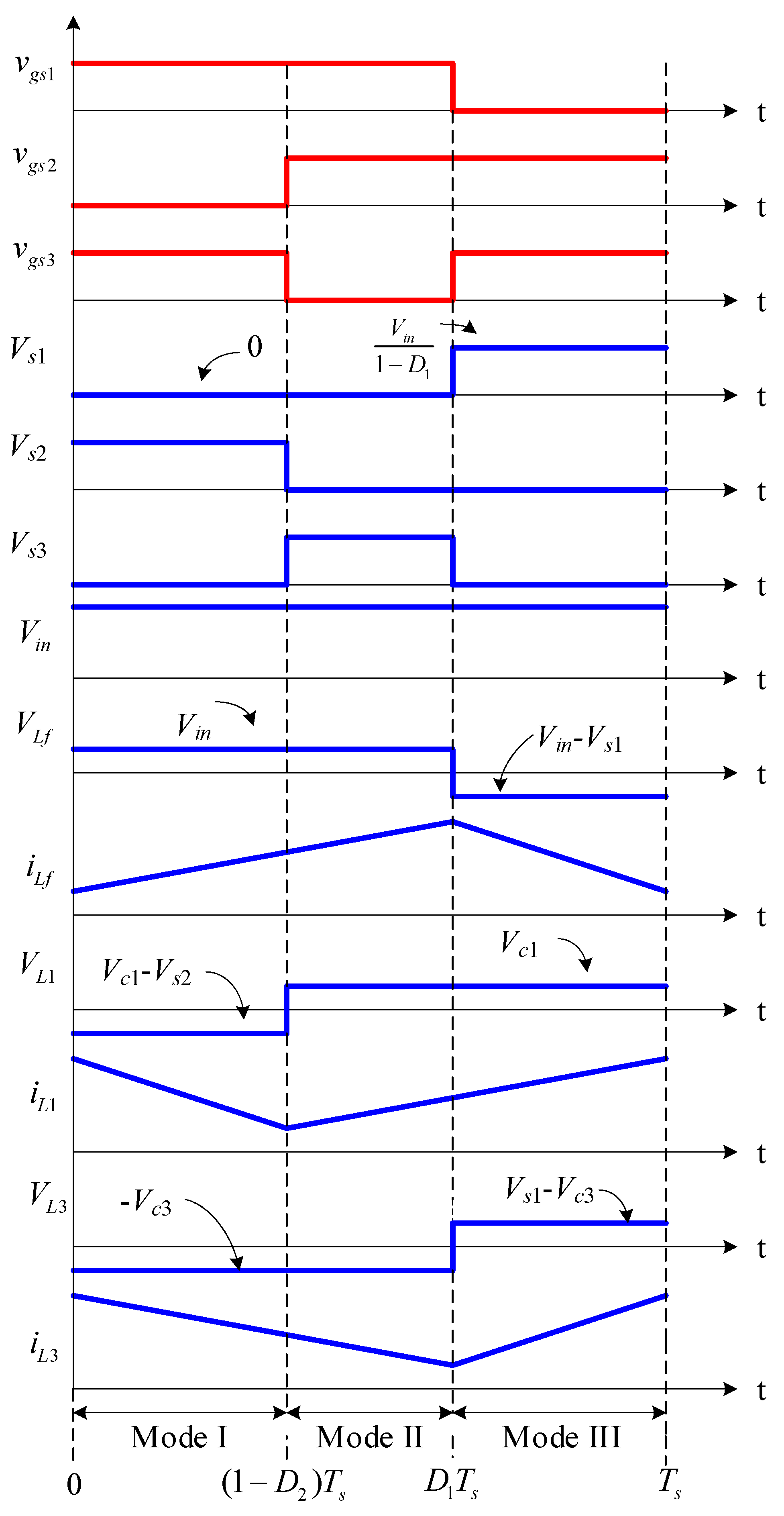
3.2. Key Waveforms in the Switching Cycle and Analysis

According to the above analysis, it is easy to get the key theoretical waveforms of the proposed topology, as shown in Figure 3. The values v g s 1 , v g s 2 , and v g s 3 are the switching statuses of switches S1, S2, and S3, respectively. The values Vs1, Vs2, and Vs3 are the voltages of switches S1, S2, and S3. When the switch is turned on, the voltage of the switch will be equal to zero. In contrast, there will be voltage in the switch when it is turned off and the value of voltage is equal to Vin(1 + k), based on Equation (16). Furthermore, VLf, VL1, and VL3 are the voltages of inductors Lf, L1, and L3, respectively. According to the operation modes in Figure 2, when D1 is at a high level, Lf is magnetized by Vin, so VLf = Vin. When D1 is at a low level, according to the loop analysis, VLf = VinVs1. As for VL1 and VL3, the same analysis method is applied and the value is shown in Figure 3. Similarly, iLf, iL1, and iL3 represent the inductors’ currents and they are changed following their voltage.

3.3. Control Diagram

Figure 4 shows the control diagram of the proposed inverter. The result of Equation (20) is a constant, it is then compared with the carrier signal to produce the switch S1 pulse, which is used to boost the input voltage. However, the result of Equation (21) is a sinusoidal variable. The driven signal of switch S2 is generated by comparing the resulting varying duty cycle with the carrier signal, which generates a sinusoidal output. According to the operation modes, only two switches are turned on at the same time. Therefore, the pulse of switch S3 can be determined by the driven signal of switches S1 and S2. The pulse of switch S3 is obtained by the XOR gate. Through the XOR gate, it is guaranteed that only two switches are turned on at a time.

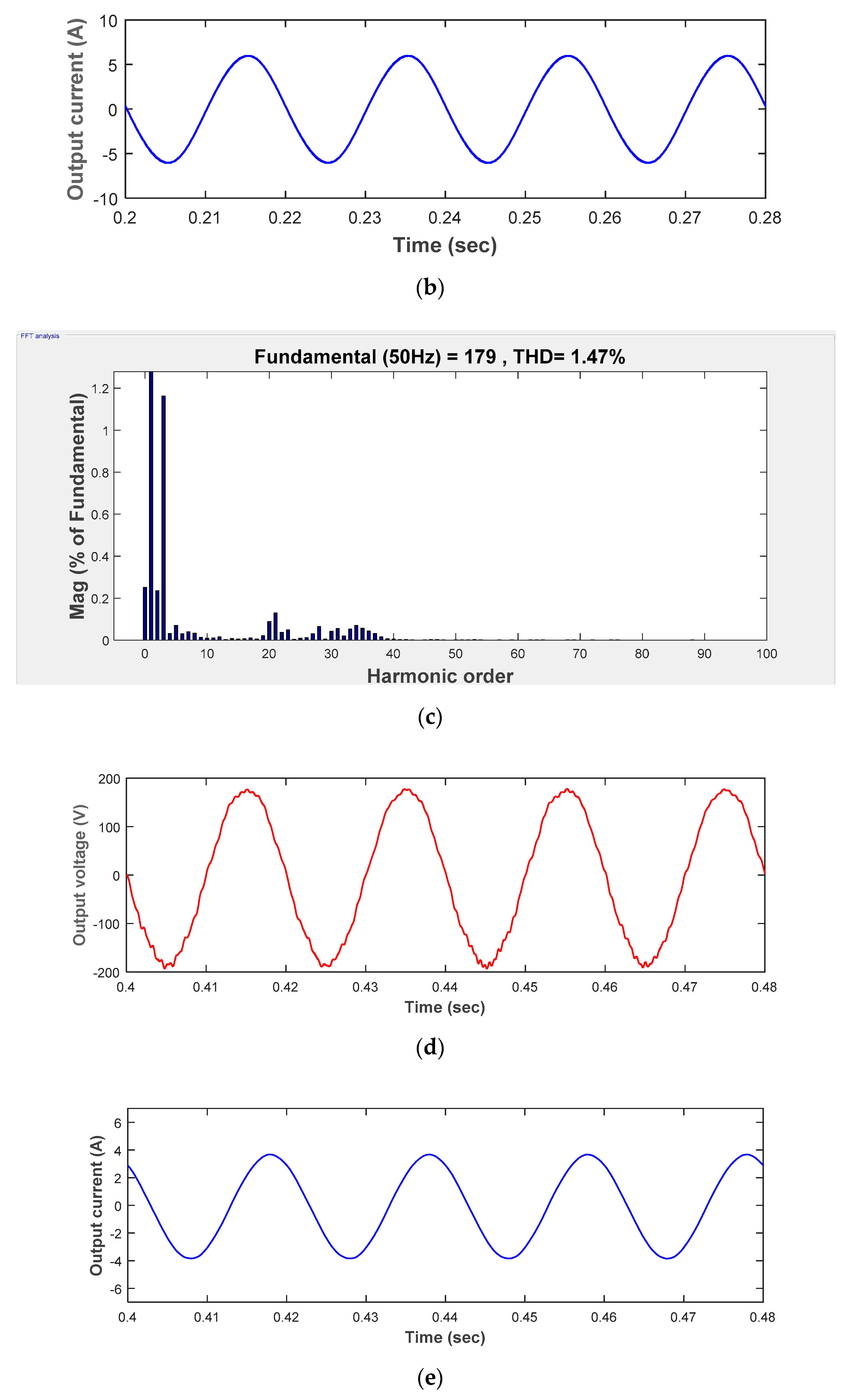
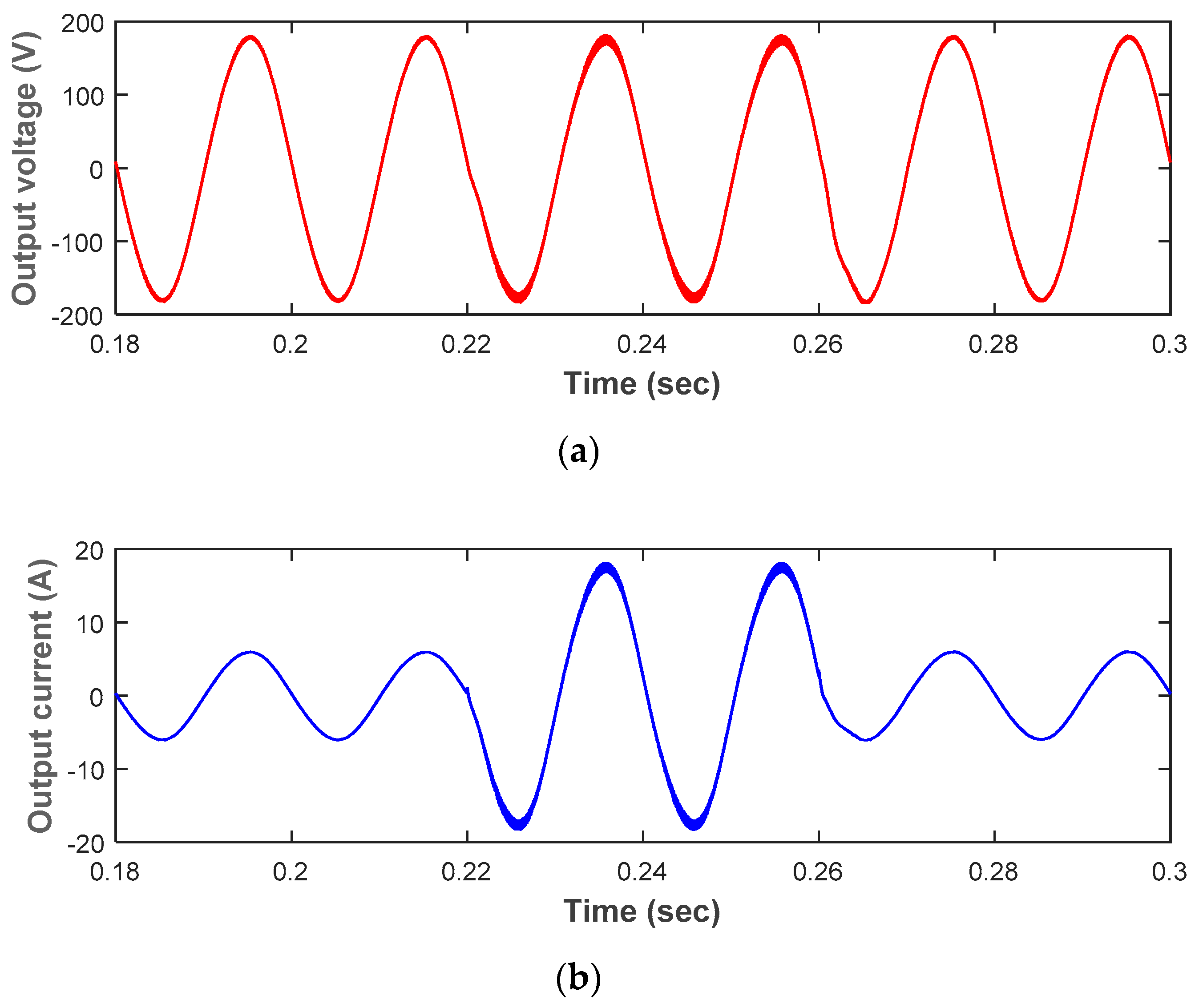
4. Simulation and Experimental Results

The simulation and experimental results of the proposed inverter are displayed in this section.

4.1. Simulation Results

The proposed inverter, under resistive load, was simulated in MATLAB/Simulink, assuming the current ripple of all inductors was calculated by Δ i L = 20 % I L . Similarly, Δ V C = 7 % V C was used to calculate the voltage ripple of all capacitors. Therefore, based on Equations (7)–(15), the value of inductors and capacitors could be calculated as shown in Table 1. Considering the laboratory conditions, in order to experiment conveniently, the switches were IGBT and the switching frequency, fs, was 20 kHz. The output of the simulation was 124 V, 50 Hz under the condition of 100 V input voltage.
Figure 5 shows the key waveforms of the proposed inverter in MATLAB/Simulink. Figure 6 shows the output voltage, output current, and Fast Fourier transform (FFT) analysis of the proposed inverter. The voltage of the capacitors is shown in Figure 7. Additionally, to better test the proposed inverter the output results of the proposed inverter are displayed in Figure 8, under the condition that the load changed suddenly.
Based on the above results, the simulation results verified the theoretical analysis. According to Figure 5, the key waveforms were consistent with the theoretical waveforms shown in Figure 3 and, at the same time, the values of the voltage satisfied the theoretical calculation. The output voltage satisfied the voltage gain and the voltage of the switches was about 300 V, which is consistent with Equation (16). Similarly, Figure 7 demonstrates Equation (7). Furthermore, the THD = 1.48%, which is well below 5%. According to Figure 8 it still worked normally, although there will be fluctuations and harmonics in the process of change. In summary, the proposed inverter can operate with satisfying performance under complex conditions.

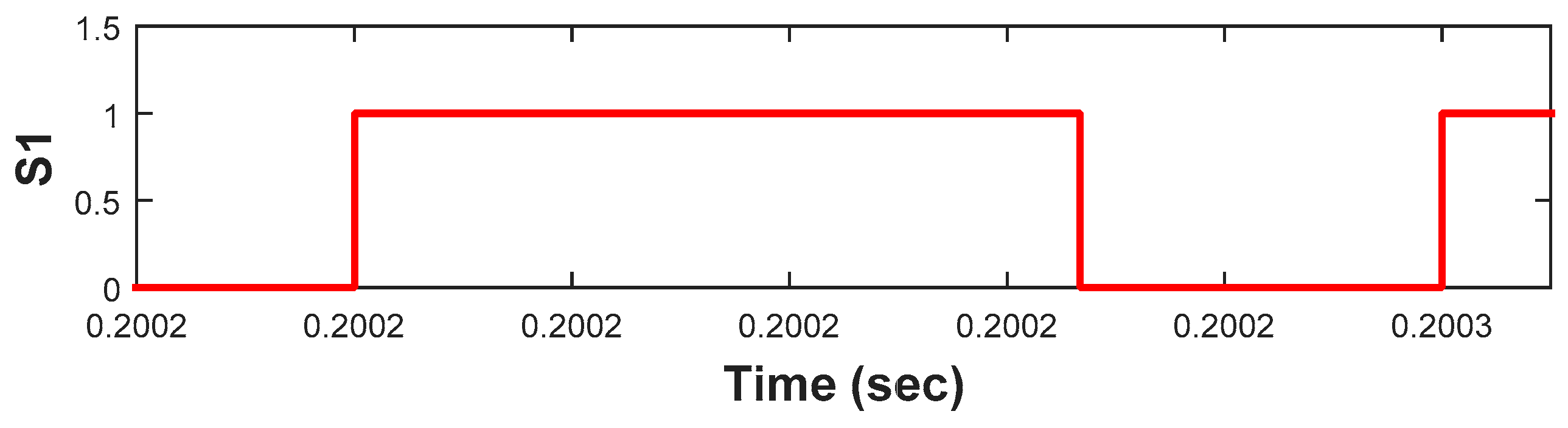
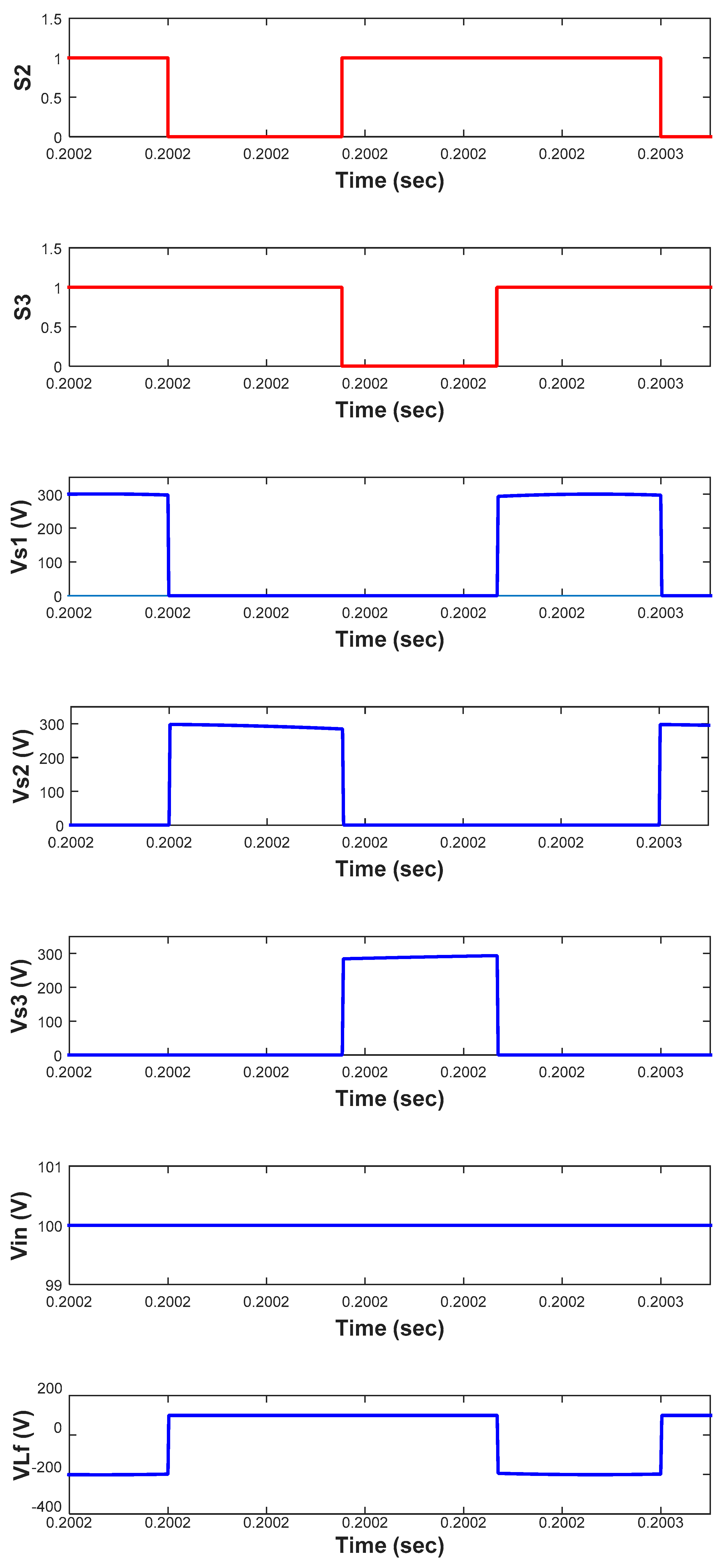
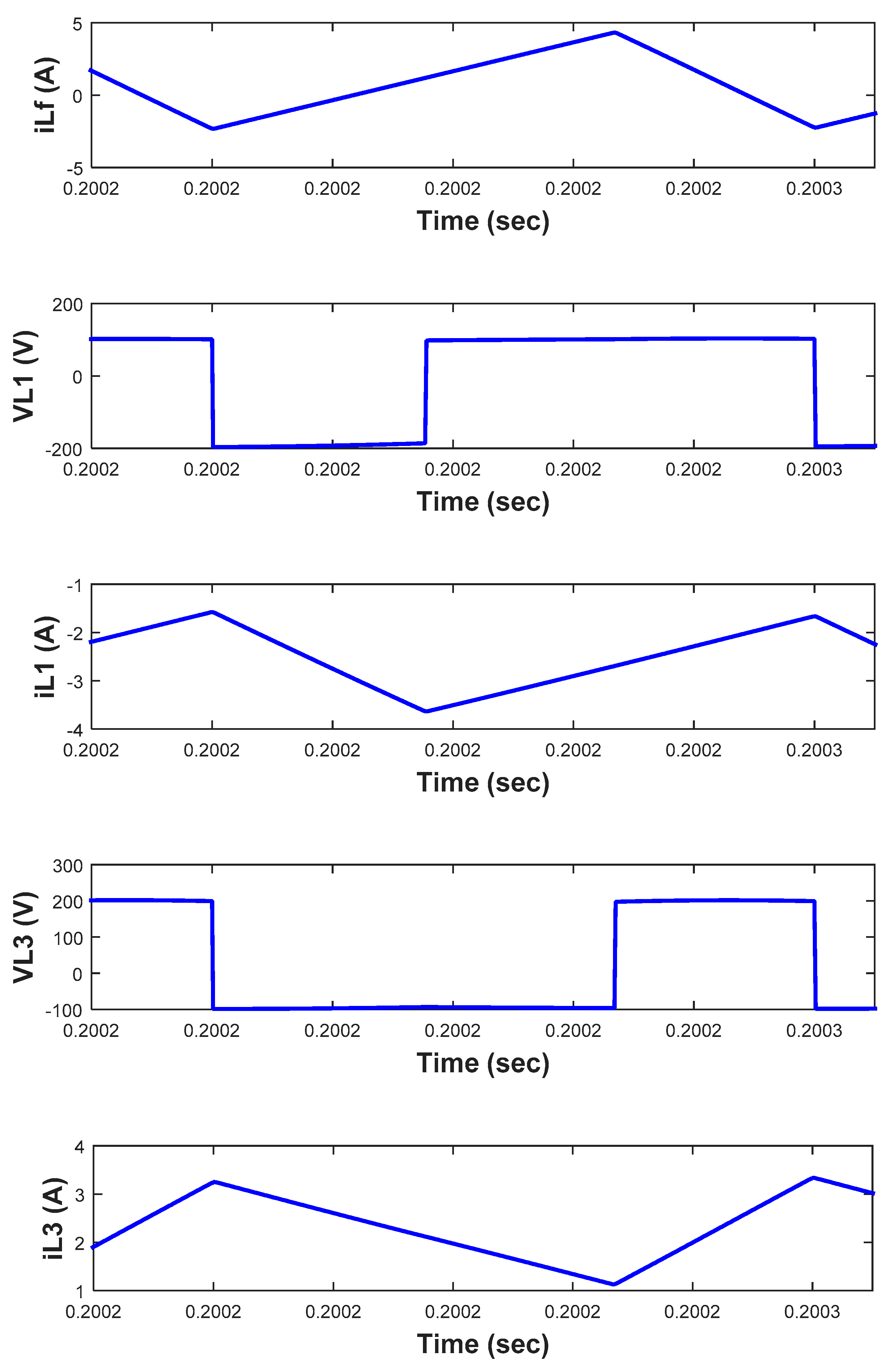
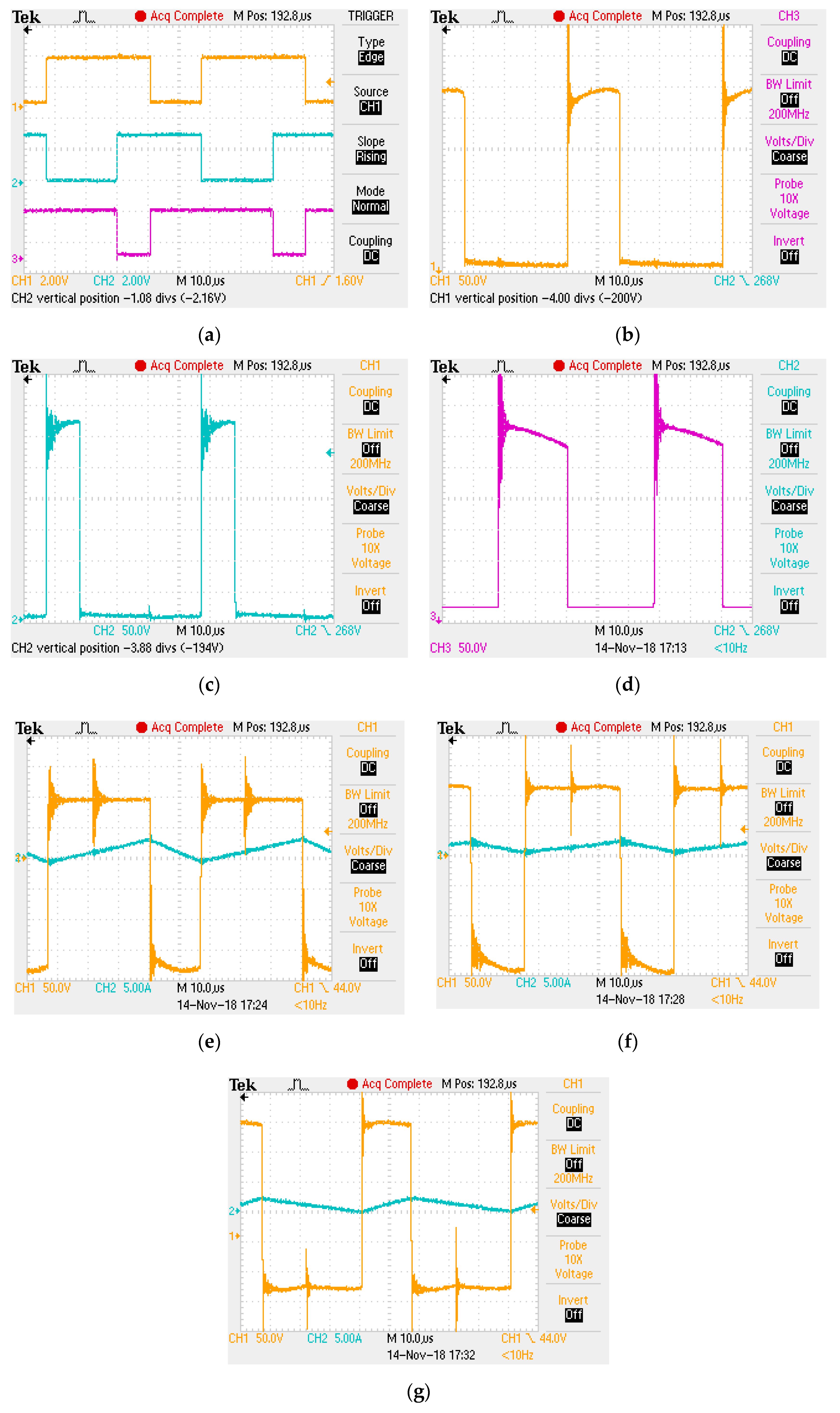
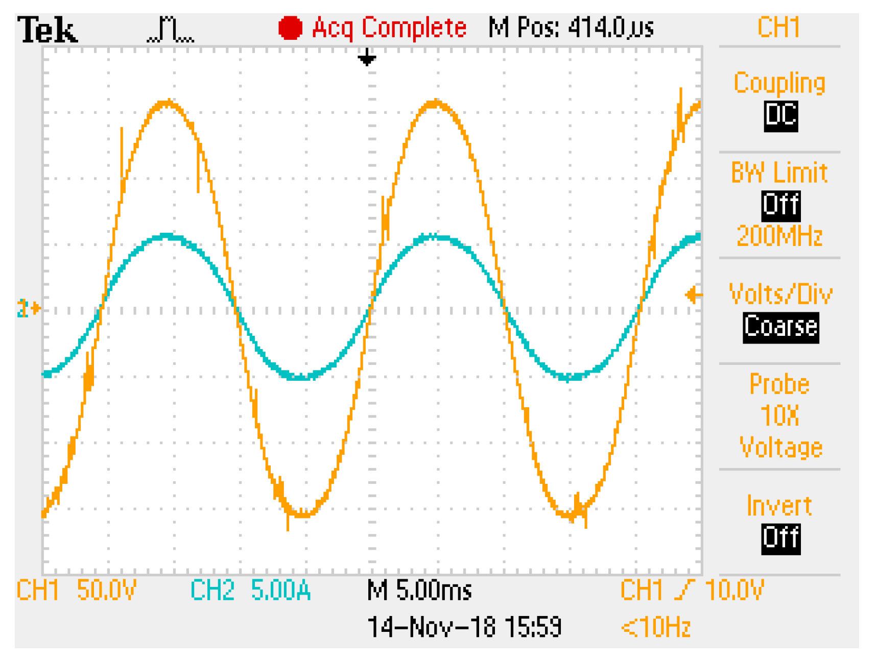
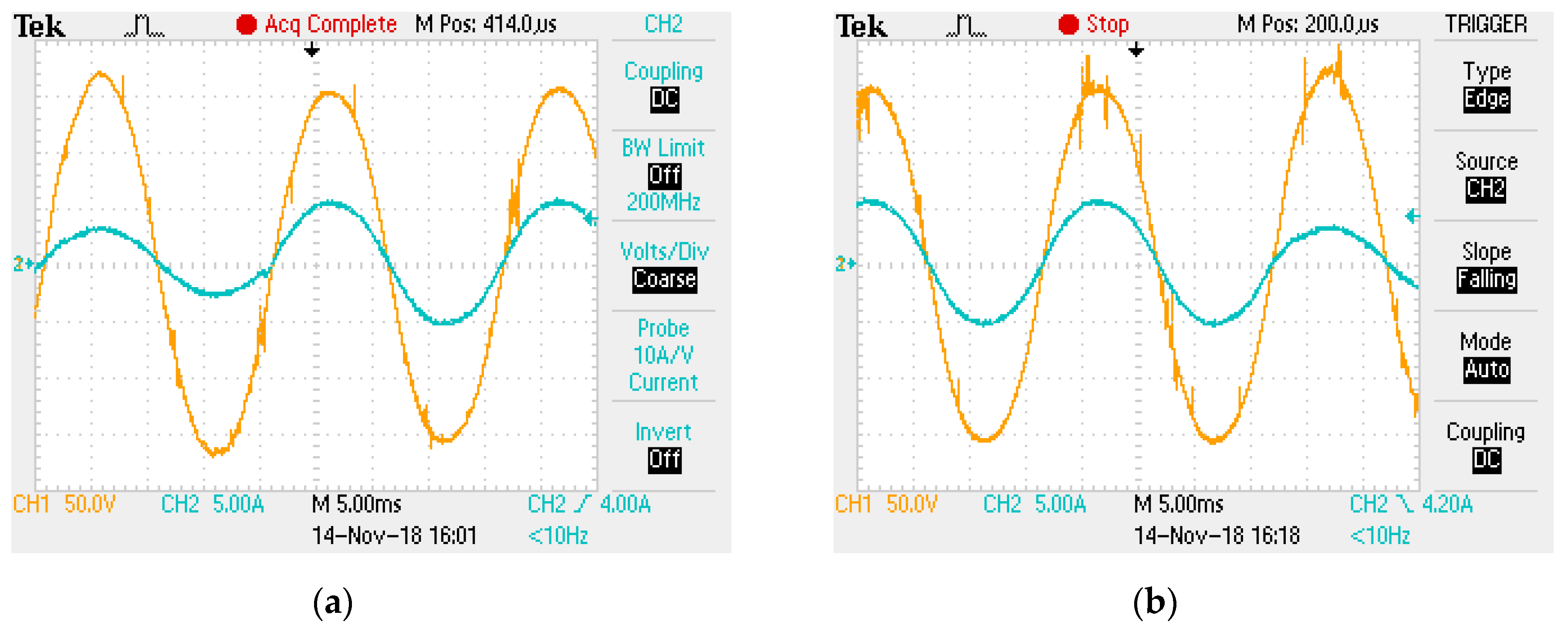
4.2. Experimental Results

The corresponding experiments were also done. The IGBT, named K40T1202 IGBT, was used for each switch in the experiment. The experimental key waveforms are shown in Figure 9. Figure 10 shows the experimental results of output voltage and output current, which correspond with Figure 6. Similarly, Figure 11 shows the experimental results of the voltage of capacitors. The experimental output waveforms of half load changed to full load and full load changed to half load are shown in Figure 12. Furthermore, in order to verify that the proposed inverter can suppress the leakage current well, a capacitor with the value of 0.15 µF was used for CPV. Figure 13 shows the experimental waveform of the leakage current.
The experimental waveforms in Figure 9 prove the theoretical key waveforms in Figure 3 and the simulation waveforms in Figure 5. Since the switches in the simulation were ideal and the experimental switches were not ideal, there are voltage spikes in Figure 9. The output voltage and current satisfied the analysis and simulation results. Furthermore, it can be seen from Figure 12 that the proposed inverter still worked well when the load changed suddenly. According to Table II in [24], compared to the traditional single-phase H4 inverter with UPWM and BPWM, the HERIC and H5 topology has lower leakage current. According to the experimental results of the HERIC topology, the max value of leakage current was more than 100 mA under the output power of 160 W. However, the leakage current of the proposed inverter was only about 48 mA under the output power of 500 W which had a good performance for eliminating leakage current and benefited from the dual-grounding.
Table 2 shows the efficiency of the proposed inverter. However, the efficiency of this topology was relatively low due to the use of IGBT as the switches, which are not appropriate for low–medium power converters, and the limitation of the laboratory conditions. A good device can be used to enhance the efficiency of the proposed topology.
In conclusion, from the above experimental results, it can be observed that the experimental results were in good agreement with the theoretical analysis and the simulation results, again verifying the effectiveness of the proposed inverter.

4.3. Comparison

In conclusion, the existing Z-source-based inverter topologies have some of the following disadvantages: complex control techniques [25,26,27], high semiconductor device counts [28,29], high numbers of capacitors and inductors [30], ripples in the capacitor voltage and inductor current [31,32,33], unsatisfactory voltage gain [34], and leakage current [35]. Table 3 shows the characteristics of different Z-source inverters. In addition, a transformer [36,37] is used to boost input voltage and isolate input and output, which will increase the cost, weight, and volume of the inverter. So, the inverter with a common ground can deal well with these problems.
In Table 3, it is easy to see that the CUK converter has low input current ripple and output current ripple, and the SEPIC converter has low input current ripple, so both CUK-based ZSI and SEPIC-based ZSI have low electromagnetic interference (EMI) [38]. Furthermore, SEPIC has the possibility of a series of resonant operations between the balancing capacitor and the parallel inductor, which can be beneficial for a soft-switching operation [39]. Therefore, SEPIC-based ZSI makes it easy to achieve a soft-switching operation.

5. Conclusions

A novel SEPIC-based Z-source inverter that eliminates leakage current is proposed in this paper. The feature of the proposed topology is a combination of a Z-source inverter and a SEPIC converter, so the current inverter has the advantages of both a SEPIC converter and a Z-source inverter, which has a high voltage gain. Furthermore, the proposed inverter is controlled by a simple linear control method, which is easy to achieve, and the proposed inverter has a low voltage stress in the switch, which is beneficial for choosing switches. Furthermore, compared with traditional single-phase H4, H5, and HERIC topologies, the proposed topology has features including fewer switches and very low leakage current, which is helpful for the application of transformerless inverters. However, the proposed topology also has the merits of the SEPIC converter. It can be seen in Figure 6 and Figure 10 that the proposed inverter has large output harmonics, due to the lack of a filter inductor. The simulation results verified the theoretical analysis. Furthermore, experiments with a laboratory prototype, using a DSP controller combined with FPGA, showed good results that were in agreement with the simulation results. The future research direction will be to study new control methods to reduce the output harmonics.

Author Contributions

This paper was a collaborative effort among all of the authors. All authors conceived the methodology, conducted the performance tests, and wrote the paper.

Funding

This work is supported by the National Natural Science Foundation of China under Grant 51777181.

Conflicts of Interest

The authors declare no conflict of interest.

Abbreviations

The following abbreviations are used in this manuscript:
Acronyms
ZSIZ-source inverter
VSIVoltage source inverter
TSTSThree-switch three-state
FFTFast Fourier transform
THDTotal harmonic distortion
SBISwitched Boost Inverters
QSBIQuasi-Switched Boost Inverters
UPWMUnipolar Pulse Width Modulation
BPWMBipolar Pulse Width Modulation
HERICHighly Efficient Reliable Inverter Concept
IGBTInsulated Gate Bipolar Transistor
SEPICSingle Ended Primary Inductor Converter
Nomenclature
APeak voltage gain
kMaximum boost radio
D 1 , D 2 , D 3 Duty cycle functions
ω Output voltage angular frequency
S1, S2, S3Semiconductor switches
V i n DC input voltage
V L i Voltage of inductors
V C i Voltage of capacitors
V s i Voltage of switches
i L i Current of inductors
i C i Current of capacitors
I o Output peak current
Δ i L i Current ripple of inductors
Δ V C i Voltage ripple of capacitors
T s Switching period
fsSwitching frequency
EMIElectromagnetic Interference

References

  1. Sulake, N.R.; Devarasetty Venkata, A.K.; Choppavarapu, S.B. FPGA Implementation of a Three-Level Boost Converter-fed Seven-Level DC-Link Cascade H-Bridge inverter for Photovoltaic Applications. Electronics 2018, 7, 282. [Google Scholar] [CrossRef]
  2. Ji, Y.; Yang, Y.; Zhou, J.; Ding, H.; Guo, X.; Padmanaban, S. Control Strategies of Mitigating Dead-time Effect on Power Converters: An Overview. Electronics 2019, 8, 196. [Google Scholar] [CrossRef]
  3. Nengroo, S.H.; Kamran, M.A.; Ali, M.U.; Kim, D.-H.; Kim, M.-S.; Hussain, A.; Kim, H.J. Dual Battery Storage System: An Optimized Strategy for the Utilization of Renewable Photovoltaic Energy in the United Kingdom. Electronics 2018, 7, 177. [Google Scholar] [CrossRef]
  4. Yu, B. An Improved Frequency Measurement Method from the Digital PLL Structure for Single-Phase Grid-Connected PV Applications. Electronics 2018, 7, 150. [Google Scholar] [CrossRef]
  5. Filippini, M.; Molinas, M.; Oregi, E.O. A Flexible Power Electronics Configuration for Coupling Renewable Energy Sources. Electronics 2015, 4, 283–302. [Google Scholar] [CrossRef]
  6. Renaudineau, H.; Donatantonio, F.; Fontchastagner, J.; Petrone, G.; Spagnuolo, G.; Martin, J.P.; Pierfederici, S. A PSO-Based Global MPPT Technique for Distributed PV Power Generation. IEEE Trans. Ind. Electron. 2015, 62, 1047–1058. [Google Scholar] [CrossRef]
  7. Xiao, G. A novel CH5 inverter for single-phase transformerless photovoltaic system applications. IEEE Trans. Circuits Syst. II Express Briefs 2017, 64, 1197–1201. [Google Scholar]
  8. Sangwongwanich, A.; Yang, Y.; Blaabjerg, F. High-Performance Constant Power Generation in Grid-Connected PV Systems. IEEE Trans. Power Electron. 2016, 31, 1822–1825. [Google Scholar] [CrossRef]
  9. Kim, K.; Cha, H.; Kim, H.G. A New Single-Phase Switched-Coupled-Inductor DC–AC Inverter for Photovoltaic Systems. IEEE Trans. Power Electron. 2017, 32, 5016–5022. [Google Scholar] [CrossRef]
  10. Meraj, M.; Iqbal, A.; Brahim, L.; Alammari, R.; Abu-Rub, H. A high efficiency and high reliability single-phase modified quasi Z-Source inverter for non-isolated grid-connected applications. In Proceedings of the IECON 2015—41st Annual Conference of the IEEE Industrial Electronics Society, Yokohama, Japan, 9–12 November 2015. [Google Scholar]
  11. Siwakoti, Y.P.; Blaabjerg, F. A novel flying capacitor transformerless inverter for single-phase grid connected solar photovoltaic system. In Proceedings of the 2016 IEEE 7th International Symposium on Power Electronics for Distributed Generation Systems (PEDG), Vancouver, BC, Canada, 27–30 June 2016. [Google Scholar]
  12. Sree, K.R.; Rathore, A.K.; Breaz, E.; Gao, F. Soft-Switching Non-Isolated Current-Fed Inverter for PV/Fuel Cell Applications. IEEE Trans. Ind. Appl. 2016, 52, 351–359. [Google Scholar] [CrossRef]
  13. Guo, X.; Jia, X. Hardware-based cascaded topology and modulation strategy with leakage current reduction for transformerless PV systems. IEEE Trans. Ind. Electron. 2016, 63, 7823–7832. [Google Scholar] [CrossRef]
  14. Zhang, L.; Sun, K.; Xing, Y.; Xing, M. H6 transformerless full-bridge PV grid-tied inverters. IEEE Trans. Power Electron. 2014, 29, 1229–1238. [Google Scholar] [CrossRef]
  15. Guo, X.; Zhang, X.; Guan, H.; Kerekes, T.; Blaabjerg, F. Three phase ZVR topology and modulation strategy for transformerless PV system. IEEE Trans. Power Electron. 2019, 34, 1017–1021. [Google Scholar] [CrossRef]
  16. Peng, F.Z. Z-source inverter. In Proceedings of the 2002 IEEE Industry Applications Conference, 37th IAS Annual Meeting, Pittsburgh, PA, USA, 13–18 October 2002; pp. 775–781. [Google Scholar]
  17. Chen, M.T.; Lin, S.H.; Cai, J.B.; Chou, D.Y. Implementing a single-phase quasi-Z-source inverter with the indirect current control algorithm for a reconfigurable PV system. In Proceedings of the IEEE International Conference on Industrial Technology, Taipei, Taiwan, 14–17 March 2016; pp. 323–328. [Google Scholar]
  18. Li, H.B.; Kayiranga, T.; Lin, X.; Shi, Y.; Li, H. A resonance suppression method for GaN-based single-phase quasi-Z-source PV inverter with high switching frequency. In Proceedings of the IEEE Energy Conversion Congress and Exposition, Montreal, QC, Canada, 20–24 September 2015; pp. 2522–2526. [Google Scholar]
  19. Ahmed, T.; Mekhilef, S.; Nakaoka, M. Single phase transformerless semi-Z-source inverter with reduced total harmonic distortion (THD) and DC current injection. In Proceedings of the IEEE ECCE Asia Downunder, Melbourne, Australia, 3–6 June 2013; pp. 1322–1327. [Google Scholar]
  20. Huang, L.; Zhang, M.; Hang, L.; Yao, W.; Lu, Z. A Family of Three-Switch Three-State Single-Phase Z-Source Inverters. IEEE Trans. Power Electron. 2013, 28, 2317–2329. [Google Scholar] [CrossRef]
  21. Li, W.; Gu, Y.; Luo, H.; Cui, W.; He, X.; Xia, C. Topology Review and Derivation Methodology of Single-Phase Transformerless Photovoltaic Inverters for Leakage Current Suppression. IEEE Trans. Ind. Electron. 2015, 62, 4537–4551. [Google Scholar] [CrossRef]
  22. Wang, B.; Tang, W. A New CUK-Based Z-Source Inverter. Electronics 2018, 7, 313. [Google Scholar] [CrossRef]
  23. Wang, B.; Tang, W. A Novel SEPIC-Based Z-Source Inverter. In Proceedings of the IECON 2018—44th Annual Conference of the IEEE Industrial Electronics Society, Washington, DC, USA, 21–23 October 2018; pp. 4347–4352. [Google Scholar]
  24. Kafle, Y.R.; Town, G.E.; Guochun, X.; Gautam, S. Performance comparison of single-phase transformerless PV inverter systems. In Proceedings of the 2017 IEEE Applied Power Electronics Conference and Exposition (APEC), Tampa, FL, USA, 26–30 March 2017. [Google Scholar]
  25. Cao, D.; Jiang, S.; Yu, X.; Peng, F.Z. Low-Cost Semi-Z-source Inverter for Single-Phase Photovoltaic Systems. IEEE Trans. Power Electron. 2011, 26, 3514–3523. [Google Scholar] [CrossRef]
  26. Nguyen, M.K.; Tran, T.T. A single-phase single-stage switched-boost inverter with four switches. IEEE Trans. Power Electron. 2017, 33, 6769–6781. [Google Scholar] [CrossRef]
  27. Ribeiro, H.; Borges, B.; Pinto, A. Single-stage DC–AC converter for photovoltaic systems. In Proceedings of the IEEE Energy Conversion Congress and Exposition, Atlanta, GA, USA, 12–16 September 2010; pp. 604–610. [Google Scholar]
  28. Nguyen, M.K.; Le, T.V.; Park, S.J.; Lim, Y.C.; Yoo, J.Y. Class of high boost inverters based on switched-inductor structure. IET Power Electron. 2015, 8, 750–759. [Google Scholar] [CrossRef]
  29. Oleksandr, H.; Carlos, R.C.; Enrique, R.C.; Dmitri, V.; Serhii, S. Single phase three-level neutral-point-clamped quasi-Z-source inverter. IET Power Electron. 2015, 8, 1–10. [Google Scholar]
  30. Caceres, R.O.; Barbi, I. A boost dc–ac converter: Analysis, design, and experimentation. IEEE Trans. Power Electron. 1999, 14, 134–141. [Google Scholar] [CrossRef]
  31. Zhou, Y.; Liu, L.; Li, H. A high performance photovoltaic module-integrated converter (MIC) based on cascaded quasi-Z-source inverters (qZSI) using eGaN FETs. IEEE Trans. Power Electron. 2013, 28, 2727–2738. [Google Scholar] [CrossRef]
  32. Sun, D.; Ge, B.; Yan, X.; Bi, D.; Zhang, H.; Liu, Y.; Abu-Rub, H.; Ben-Brahim, L.; Peng, F.Z. Modeling, impedance design, and efficiency analysis of quasi-Z source module in cascade multilevel photovoltaic power system. IEEE Trans. Ind. Electron. 2014, 61, 6108–6117. [Google Scholar] [CrossRef]
  33. Tang, Y.; Xie, S.; Ding, J. Pulsewidth modulation of Z-source inverters with minimum inductor current ripple. IEEE Trans. Ind. Electron. 2014, 61, 98–106. [Google Scholar] [CrossRef]
  34. Vazquez, N.; Rosas, M.; Hernandez, C.; Vazquez, E.; Perez-Pinal, F.J. A New Common-Mode Transformerless Photovoltaic Inverter. IEEE Trans. Ind. Electron. 2015, 62, 6381–6391. [Google Scholar] [CrossRef]
  35. Nguyen, M.-K.; Le, T.-V.; Park, S.-J.; Lim, Y.-C. A Class of Quasi-Switched Boost Inverters. IEEE Trans. Ind. Electron. 2015, 62, 1526–1536. [Google Scholar] [CrossRef]
  36. Nguyen, M.K.; Lim, Y.C.; Park, S.J. Improved trans-Z-source inverter with continuous input current and boost inversion capability. IEEE Trans. Power Electron. 2013, 28, 4500–4510. [Google Scholar] [CrossRef]
  37. Nguyen, M.K.; Lim, Y.C.; Park, S.J.; Shin, D.S. Family of high-boost Z-source inverters with combined switched-inductor and transformer cells. IET Power Electron. 2013, 6, 1175–1187. [Google Scholar] [CrossRef]
  38. Veerachary, M. Power tracking for nonlinear PV sources with coupled inductor SEPIC converter. IEEE Trans. Aerosp. Electron. Syst. 2005, 41, 1019–1029. [Google Scholar] [CrossRef]
  39. Hasanpour, S.; Baghramian, A.; Mojallali, H. A Modified SEPIC-Based High Step-Up DC-DC Converter with Quasi-Resonant Operation for Renewable Energy Applications. IEEE Trans. Ind. Electron. 2019, 66, 3539–3549. [Google Scholar] [CrossRef]
Figure 1. Proposed SEPIC-based Z-source inverter (ZSI).
Electronics 08 00247 g001
Figure 2. Equivalent circuits of the SEPIC-based ZSI in one switching period (a) S1 and S3 are ON, S2 is OFF; (b) S1 and S2 are ON, S3 is OFF; and (c) S2 and S3 are ON, S1 is OFF.
Electronics 08 00247 g002
Figure 3. Key waveforms in one switching period.
Electronics 08 00247 g003
Figure 4. Control block diagram of the proposed inverter.
Electronics 08 00247 g004
Figure 5. Key waveforms of the proposed inverter in MATLAB.
Electronics 08 00247 g005aElectronics 08 00247 g005bElectronics 08 00247 g005c
Figure 6. Input voltage at 100 V and load at 30 Ω for SEPIC-based ZSI: (a) load voltage, (b) load current, (c) Fast Fourier transform (FFT) analysis, (d) output voltage with inductive load, and (e) output current with inductive load.
Electronics 08 00247 g006aElectronics 08 00247 g006b
Figure 7. Input voltage at 100 V and load at 30 Ω for SEPIC-based ZSI. Voltage wave of (a) capacitor C1, (b) capacitor C2, (c) capacitor C3, and (d) capacitor C0.
Electronics 08 00247 g007
Figure 8. Input voltage at 100 V and load changed (30–10–30 Ω) for SEPIC-based ZSI: (a) load voltage and (b) load current.
Electronics 08 00247 g008
Figure 9. Experimental waveforms: (a) driven signal of the switches; (b) the voltage of switch S1 (CH1: Time (10 µs/div), Vs1 (50 V/div)); (c) the voltage of switch S2 (CH2: Time (10 µs/div), Vs2 (50 V/div)); (d) the voltage of switch S3 (CH3: Time (10 µs/div), Vs3 (50 V/div)); (e) the voltage and current of inductor Lf (CH1: Time (10 µs/div), VLf (50 V/div), CH2: Time (10 µs/div), iLf (5 A/div)); (f) the voltage and current of inductor L1 (CH1: Time (10 µs/div), VL1 (50 V/div)), CH2: Time (10 µs/div), iL1 (5 A/div)); and (g) the voltage and current of inductor L3 (CH1: Time (10 µs/div), VL3 (50 V/div), CH2: Time (10 µs/div), iL3 (5 A/div)).
Electronics 08 00247 g009
Figure 10. Input voltage at 100 V and load at 30 Ω. Experimental waveforms of v o (CH1: Time (5 ms/div), v o (50 V/div)) and Io (CH2: Time (5 ms/div), Io (5 A/div)).
Electronics 08 00247 g010
Figure 11. Input voltage at 100 V and load at 30 Ω. Experimental waveforms of (a) V c 1 (CH1: Time (5 ms/div), V c 1 (50 V/div)) and V c 2 (CH2: Time (5 ms/div), V c 2 (50 V/div)); (b) V c 3 (CH3: Time (5 ms/div), V c 3 (50 V/div)) and V c 0 (CH4: Time (5 ms/div), V c 0 (50 V/div)).
Electronics 08 00247 g011
Figure 12. Input voltage at 100 V and sudden load changes: (a) from 60 to 30 Ω, (b) from 30 to 60 Ω. Experimental waveforms of v o (CH1: Time (5 ms/div), v o (50 V/div)) and Io (CH2: Time (5 ms/div), Io (5 A/div)).
Electronics 08 00247 g012
Figure 13. The waveform of leakage current (CH2: I (50 mA/div)).
Electronics 08 00247 g013
Table 1. Parameters selected for the inverter simulation.
ParametersVin (V)Vo (rms, V)fs (kHz)A (Voltage Gain)kL3 (mH)Lf (mH)L1, L2 (mH)C0 (µF)C1, C2 (µF)C3 (µF)
value100124201.7521.50.51.6537.6159
Table 2. The measured efficiency of the proposed inverter.
Output power (W)120204.5311358431
Efficiency (%)89.990.0891.1791.7089.58
Table 3. Comparison between different Z-source inverters. EMI: electromagnetic interference.
LCDSControl MethodVoltage GainCommon GroundEMISoft Switch
Semi-ZSI [25]2202nonlinear<1Yeshighcomplex
Semi-ZS-based [34]3302linear<1Yeshighcomplex
Basic SBI [35]1122linear>1Nohighcomplex
Embedded-type qSBI [35]1122linear>1Nohighcomplex
DC-linked-type qSBI [35]1122linear>1Nohighcomplex
CUK-based ZSI [22]4403linear>1Yeslowcomplex
Boost-based ZSI [20]3303linear>1Yeshighcomplex
Buck–boost-based [20]3303linear>1Yeshighcomplex
Proposed in [23]4403linear>1Yeslowsimple

