Article

Experimental Study on the Reliability of PBGA Electronic Packaging under Shock Loading

1
China Aero-Polytechnology Establishment, Beijing 100028, China
2
China Jiangsu Province Key Laboratory of Aerospace Power System, Nanjing University of Aeronautics and Astronautics, Nanjing 210016, China
*
Author to whom correspondence should be addressed.
Electronics 2019, 8(3), 279; https://doi.org/10.3390/electronics8030279
Submission received: 27 December 2018 / Revised: 22 February 2019 / Accepted: 23 February 2019 / Published: 2 March 2019
(This article belongs to the Section Systems & Control Engineering)

Abstract

:
Plastic Ball Grid Array (PBGA) one of the most important electronic packaging methods, is widely used in aeronautical industry field. According to the JEDEC standard, shock tests of PBGA assemblies are conducted under different loading conditions. Several important parameters, such as the fatigue life of PBGA assemblies, the relationship between solder joint positions and fatigue life, the relationship between strain energy density and fatigue life, are analyzed based on experiment results. The failure modes of PBGA assemblies are studied by optical microscope (OM). The results show that during the shock tests, the strains of the solder joints near the center of the specimen are larger than other positions, and these solder joints are prone to form micro cracks. With the increase of the shock times, these micro cracks extend rapidly which will eventually cause the failure of the PBGA electronic packaging.

1. Introduction

Ball Grid Array (BGA) Package technology is one of the most important and popular electronic packaging methods in the modern electrical and aeronautical industry field and it has many advantages such as good heat matching, low costs, good electrical properties, etc. [1]. During its usage period in the aircraft, mechanical shock loading is very common, the research on reliability under shock loading is very important for avionics electronic products.
Early attention to the reliability problem of microelectronics packaging under thermal and mechanical shock loading is designated to foreign communications companies such as Motorola, Lucent technologies. Wu and Song [2] studied the drop shock influence on communication products by means of experiment and simulation. Goyal and his colleagues of Lucent technologies studied the drop shock influence on thin-walled shell phone by a drop shock test and found that cell phone shell stiffness was insufficient under the action of shock loading, and components were prone to crack, and the shape and size of the mobile phone’s effects on component failure were extremely significant [3]. In order to simulate the product process more realistically, Goyal and Buratynski [4,5] proposed a new drop testing instrument. Ong Y C studied drop shock testing on the Nokia 3210 mobile phone in the product level and board level [6]. Tong Yan Tee and Jing-en Luan proposed Input-G model in the board-level drop simulation [7,8,9,10]. Desmond Y R compared the shock resistance of PBGA (plastic ball grid array), VQFN (very thin quad flat no-lead), and PQFP (plastic quad flat pack) packaging components, and the results showed that VQFN solder joints’ shock resistance was the best [11]. In China, many scholars have also done a lot of board level drop test and simulation work on electronic packaging successively. Zhou Dejian and Pan Kailin carried on the theoretical analysis and dynamic simulation on reliability problems in the drop shock of Thin Fine-Pitch Ball Grid Array (TFBGA) encapsulation component [12,13]. Qi Bo and Wang Jiaji studied the drop shock test on BGA encapsulation component, and analyzed microstructure and composition of the failure solder by SEM/EDX BGA [14,15]. Zhu Zhenjun and Zhao Mei studied the dynamic responses of PBGA solder joints under the environment of earthquake [16]. Qin Fei and Bai Jie established three dimensional finite element models of BGA encapsulation component by finite element software ANSYS and did simulation analysis on the deformation of printed circuit board (PCB) and the stress of solder joints by the method of Input-G [17,18]. Liu Weisheng did finite element drop simulation analysis of electronic chassis on the PCB using ANSYS/LS-DYNA, and simulated the whole process of drop shock, analyzing the drop height and cushion effect on the dynamic response of the PCB board [19]. Zhang Jie and Yang Ping studied effects of PBGA components’ structure factors such as parameters and material properties on the solder joint stress by a combination of analytical method and finite element analysis [20]. Yau, Y.H, Mattila, T.T and Zhang, B. studied the dynamic mechanism of electronic devices, board under the drop impact [21,22,23].
This paper uses the Input-G method to conduct shock test on PBGA packaging PCB in board level following the JEDEC (Joint Electron Device Engineering Councils) standard. The failure modes of solder joints were determined and the failure lives of the solder joints were obtained by monitoring the current voltage signal of solder joints after the shock test. The strain of each component was obtained by using dynamic data acquisition instrument monitoring dynamic strain of PCB, S-N curve and P-S-N curve of solder joints were established. The static failures of solder joint were observed through the optical microscope and the failure reason of solder joints was analyzed.

2. Test Design

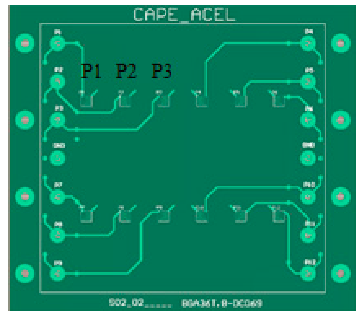
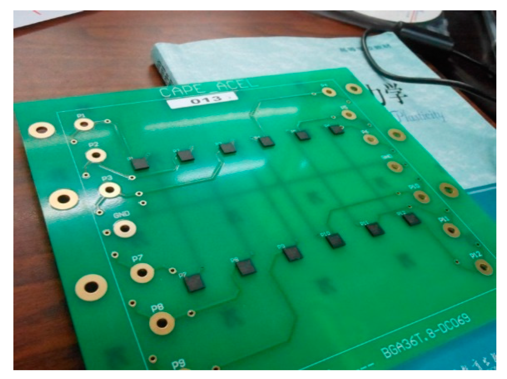
2.1. Test Sample Design

The test sample of printed circuit board (PCB) consists of 12 PBGA packaging devices and the design is shown as Figure 1. The real figure is shown as Figure 2. The length, width and thickness of the PCB boards are 180 mm, 160 mm, and 2 mm individually, and the length and width of the PBGA packaging devices are both 21 mm. Each PBGA has 36 solder joints, and the diameter is 0.5 mm. The process parameters are as shown in Table 1.
When installing the PCB during the test, it is important to ensure good welding of the signal line of the PCB and line hole of corresponding substrate to ensure good welding. Then, the transfer-base-table was fixed in the shock amplifier, the samples were fixed with hexagonal stainless steel bolt, and the sensor was tightened in amplifier to ensure firm without loose. Finally, signal and sensor lines were taped respectively on the table to prevent excessive force to cause damage or fracture in the process of shock, which is shown as Figure 3.

2.2. Test Loading

CL-20 impact test stand was used and the loading parameters are shown as Table 2.
JEDEC standard JESD22-B111 ’Board Level Drop Test Method of Components for Handheld Electronic Products’ was used, and the typical shock test pulse of the standard is shown as Figure 4, and the formula is described as:
A ( t ) = A 0 sin ( π t t w )
where A0 is shock wave peak, and tw is shock wave pulse width.
Test condition of JESD22-B110 is list as Table 3. Here test sample No. 013, 027, 035, and 036 use condition B, namely peak acceleration is 1500 g and pulse duration is 0.5 ms, test sample No. 026, 028, 030, and 033 use condition G, the peak acceleration is 2000 g and pulse duration is 0.4 ms, test sample No. 025 and 029 used condition H, the peak acceleration is 2900 g and pulse duration is 0.3 ms.
The sampling frequency of high-speed dynamic data acquisition instrument for testing should be less than 50 KHZ. If a daisy chain resistance is larger than 100 Ω for the first time, the lasting time is larger than 1μs, and the same phenomenon occurs larger than 2 times in the subsequent 5 times fall, the failure is defined as a transient failure in JEDEC standard. With the increase of falling number, the daisy chain resistance will increase, if larger than 1000 Ω, and it is defined as a static failure.

3. Monitoring of Test Data

In order to monitor the shock failure life of the solder joint, the real-time resistance of solder daisy chain needs to be monitored. Considering the difficulty of achieving the dynamic resistance monitoring, the real-time monitoring of solder joints can be achieved through a series of known resistance and monitoring voltage value of known resistance. Related transformation formula is shown as Equation (2).
R 0 = R x ( E V ) V
where, R0 is a known resistance as 150 Ω, Rx is daisy chain resistance, E is the total voltage and V is voltage of R0. JEDEC standard shows that when the measured voltage is less than 3 V for 3 times in 5 times test, it is considered as a static failure. When the test voltage is less than 0.65 V and it is judged as a static failure. Voltage signal is acquired by Agilent U2531A high speed data acquisition system. The power output voltage value is set to 5 V. Current of Path is 0.142 A. Then real-time acquisition and data storage are done through the system software.
Strain detection was collected by DH5922 dynamic data acquisition instrument. Strain gages were sticked at the side of the PCB components without elements. During the process of dropping shock, the electrical measuring method was used to study the strain changes of PCB components, that was installed horizontally and its package was installed face down. Strain gage adopts BX120-2CA resistance strain gage with the resolution is 1% με, and the length and width of the sensitive gate are 2 mm and 1 mm, and the length and width of the base are both 7.2 mm. The strain gage, which was sticked on the side of the PCB without components, was constructed testing bridge arm through strain modulator. Figure 5 is the shock test site.

4. Test Data Analysis

4.1. Data Analysis

The monitored devices in the test are P1, P2, and P3, which are shown in Figure 1. Partial data of the maximum values of strain, the number of first transient failures and the number of first static failures for one board in the drop shock test are shown in Table 4. The comparison of the results are analyzed as Figure 6.
With the increase of shock loading, the stress and strain of PCB board increases, and the life of solder joint is obviously reduced. At higher stress levels, the life of the solder joints at points P2 and P3 are similar and it is difficult to capture the transient failure of the solder joints. At the same strain of the test board, the number of the first transient failure and static failure decrease gradually with the strain increasing. And because the positions of P1, P2, and P3 are gradually near to the center, the strain gradually increases. Under the low shock, the reliability of P1 is larger than P2 and P3, because the position of P2 and P3 are more closed to the center, the test board can also produce large strain under the low shock. In order to ensure the product reliability, the P2 and P3 shock resistance need to be improved.
Figure 7 shows comparison of numbers of first time transient and static failures for the P1, P2, and P3, where the abscissa coordinate is the strain, the vertical coordinate is the failure times. The number of first transient failures and the number of first static failures decrease gradually with the increase of strain at the same point. When the transient failure occurs about 10 to 100 times, the static failure occurs. That is, when a certain amount of cracks occurs, the stress concentrations at the crack cause the crack propagation rate to be high, leading to the formation of large cracks, which leads to the failure of the solder joints.

4.2. Stress–Life Analysis

The stress–life relationship of the test sample can be expressed by the following formula,
a + b lg σ max = lg N
where, a and b can be obtained by least squares fitting using Matlab software, the data σmax and N are in Table 4, and the stress-transient failure life of the formula a = 1.7, b = −0.2173. Then the stress-transient failure life curve is shown as Figure 8. In the stress-static failure life formula, parameters a = 1.526, b = −0.1381 and the curve is shown as Figure 9.
It can be seen from Figure 8 and Figure 9 that the experimental data are close to the theoretical values at high stress levels, which is similar to the fatigue properties of general materials.

4.3. Strain Energy Contrast Analysis

Strain energy density can be expressed by the following formula,
U = 1 2 σ ε
where σ is obtained from the following equation and here E = 1.11 × 10¹⁰ Pa, μ = 0.28.
σ = Ε 2 [ ε 0 + ε 90 1 μ + 1 1 + μ ( ε 0 ε 90 ) 2 + ( 2 ε 45 ε 0 ε 90 ) 2 ]
The energy produced by all location point of all boards of the first static failure and transient failure is shown in Table 5.
The strain energy density of each solder joints during static failure is shown as Figure 10. The total strain energy density of P1, P2, and P3 in high stress region is relatively stable. P2 and P3 are influenced by solder reflow process, so the dispersion in low stress region is larger, and the result is more concussion. But the sum of the strain energy of the PCB in the high stress region is relatively conserved.
The strain energy density formula can be approximated as:
U = 1 2 σ 2 E
Considering the influence of energy on the life, the stress-life formula and the above equation are combined and we obtain,
lg N = a + b 2 lg U + b 2 lg 2 E
The data in Table 5 and Table 6 are substituted into the above formula, and the parameters a′ = 5.234 and b′ = −0.4474 in the formula of strain energy density-life can be obtained by fitting and the strain energy density–life curve is shown as Figure 11. It can be seen that the trend of strain energy density and stress on life is close.

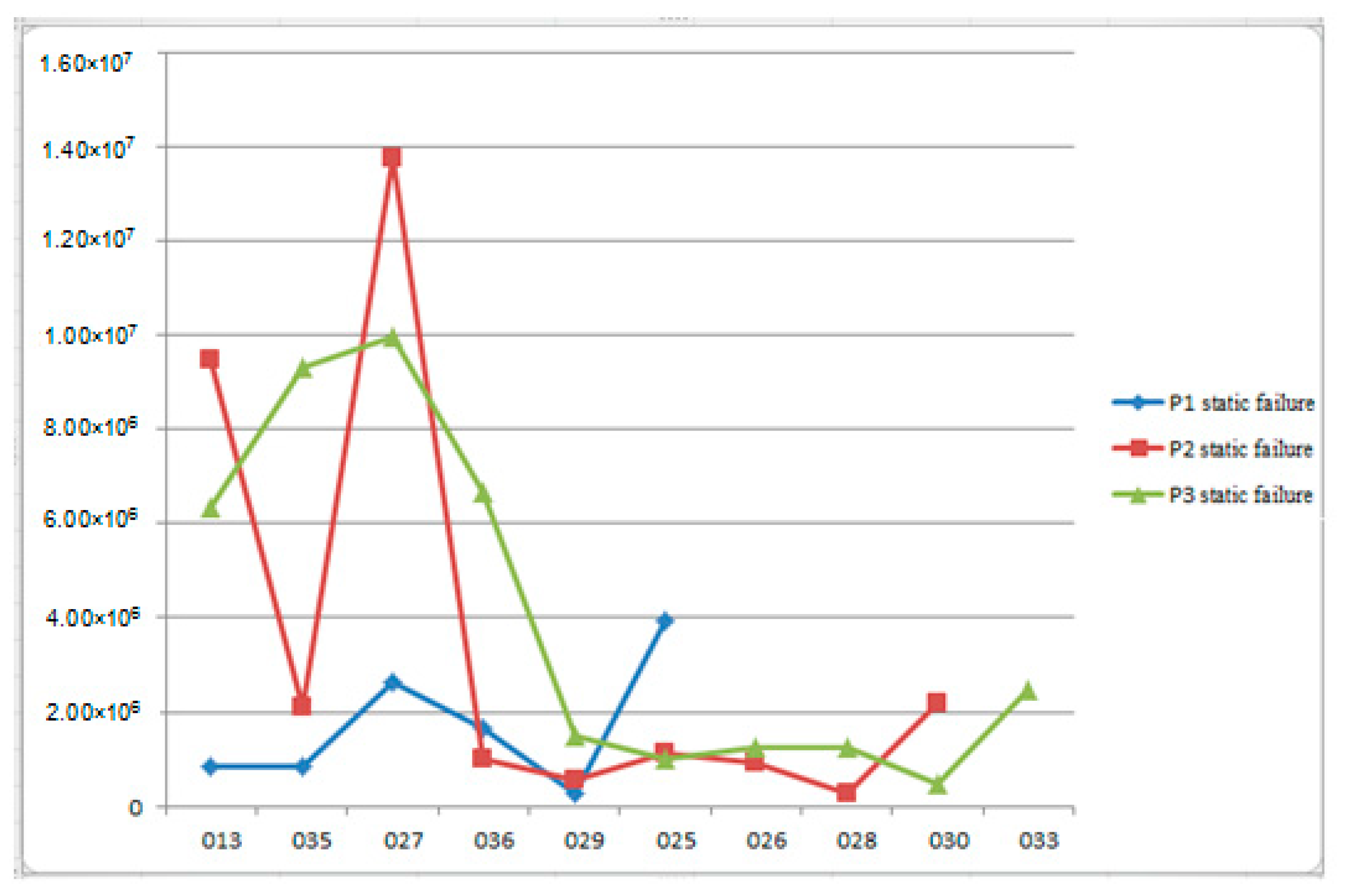
4.4. Solder Joint Reliability Analysis
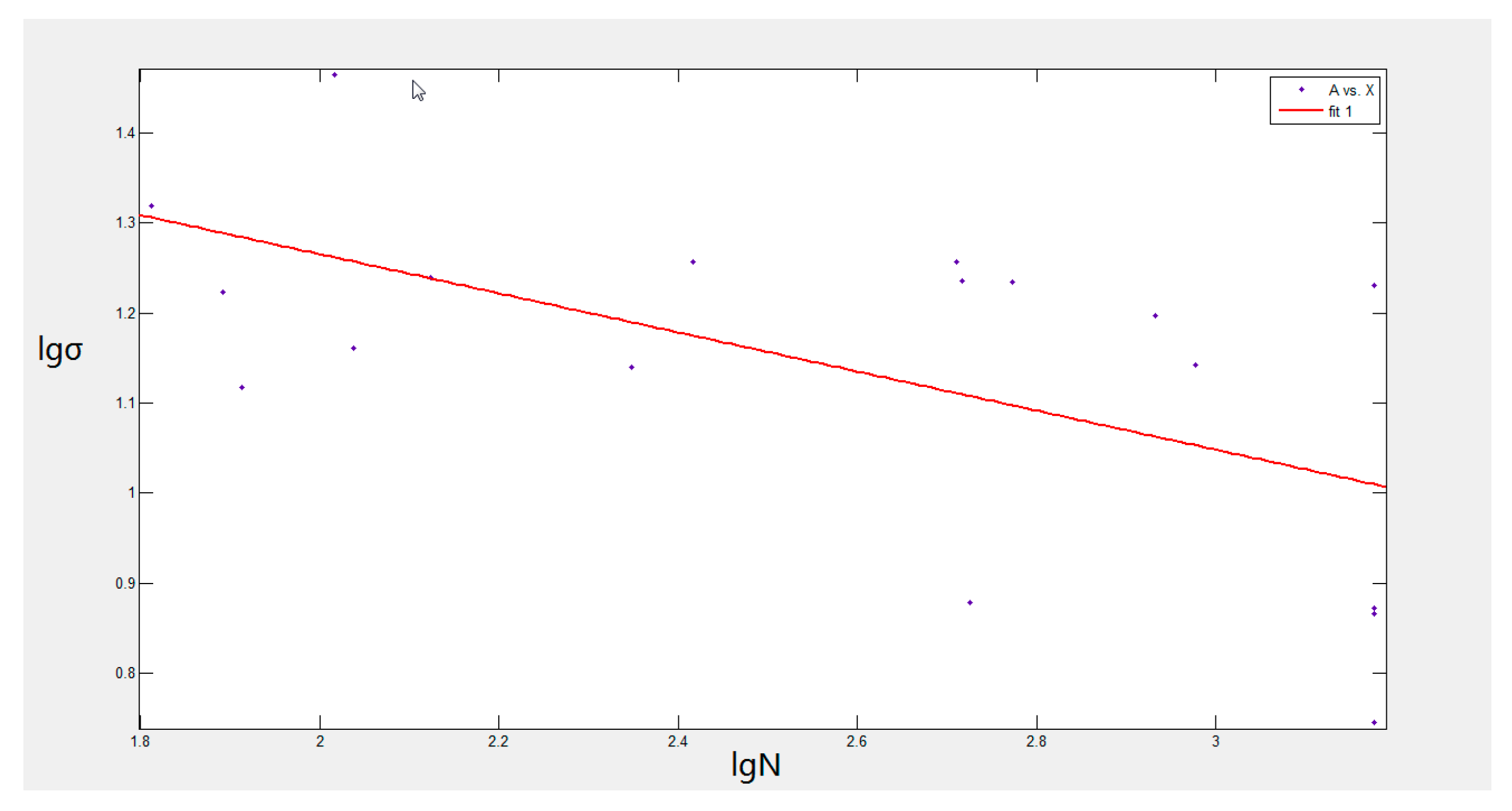
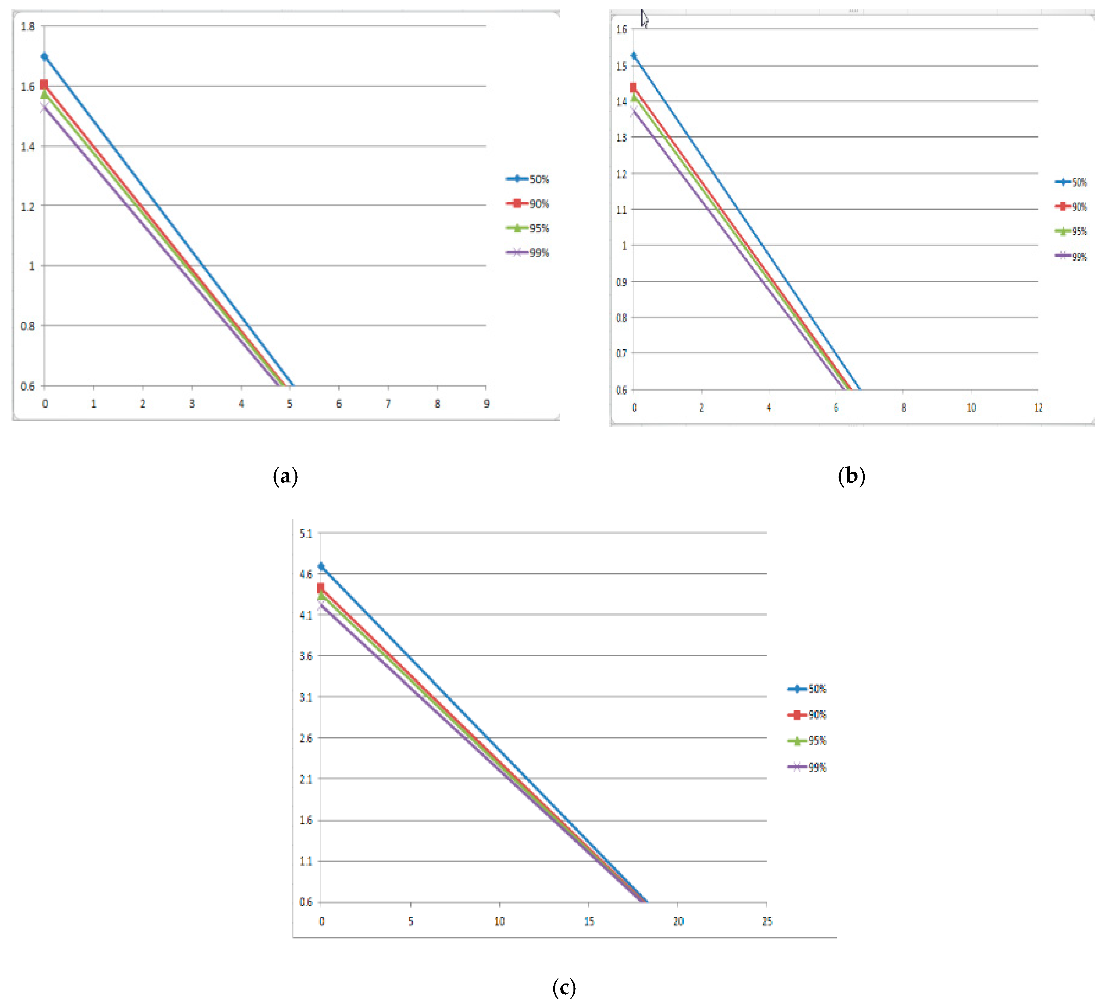
Assuming that the reliability of solder joints obeys the Weibull distribution, and the distribution density function is:
f ( t ) = m η ( t η ) m 1 e ( t η ) m
By integrating f(t), the failure distribution function F(t) can be obtained:
F ( t ) = 1 e ( t η ) m
The original equation can be converted to:
lg lg [ 1 F ( t ) ] 1 = m lg t m lg η
The left side of the equation is the failure rate and lgt is the lifetime. Consider board 013, 035, 027, 036 use B test condition, board 029, 025 use H test condition, board 026, 028, 030, 033 use G test condition. Through the data fitting, the relationship between failure rate of the test board and lifetime under B and H test conditions is obtained, and it is shown in Figure 12.
When the failure rate is 63.2%, the life is the characteristic life, then transient and static characteristics life of the test conditions are shown as Table 6.

4.5. P-S-N Curve

Considering the experiment belonging to the small samples, the reliability of its confidence of the Probabilistic Stress-Life (P-S-N) curve need to be considered. Combined the relevant references, the fatigue life NP,Y can be expressed as following:
lg N P , Y = lg N ¯ ( 1 L P , Y C V )
Which lg N ¯ is the mean of logarithmic fatigue life; L P , Y is the single-margin factor and can be obtained through the look-up table; CV is the empirical statistics.
Considering the practical requirements, the confidence γ is chosen to be 90%. This paper presents safety probability in 90%, 95%, and 99% of P-S-N curve. The selected number of samples ni is 29, for welding components, C V is 0.035, and single-sided statistical allowable coefficient table of the normal distribution shows that the values of L P , Y under 90%, 95%, and 99% safe probability are: 1.655, 2.089, and 2.896. Then transient failure PSN curve equation can be calculated by the equation 12. Figure 13 shows the transient failure P-S-N curve. By the same methods, the static failure P-S-N curve and the strain energy-lifetime P-U-N curve are required as Figure 13.
From the above figures, the curves in the corresponding curve family are arranged in parallel, and the closer the curve is to the vertical axis, the higher the safety probability is.

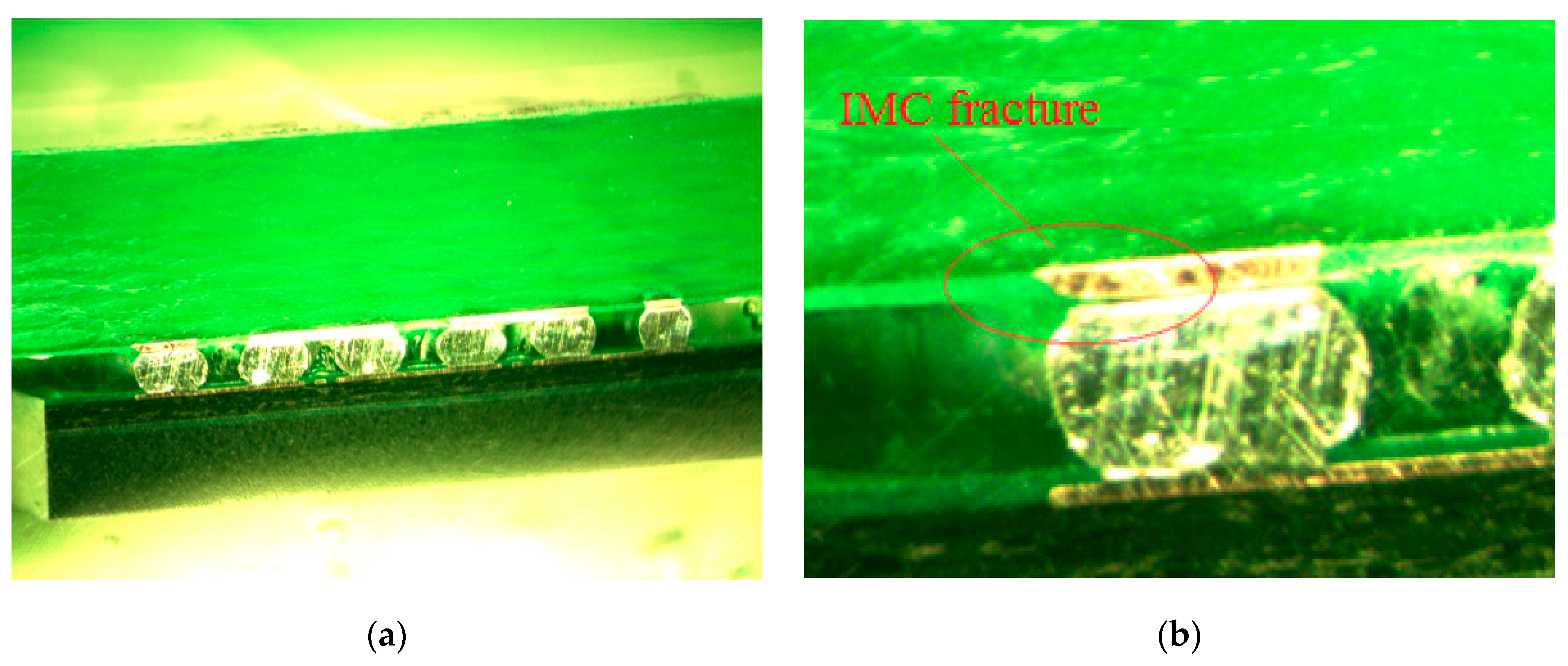
4.6. Microscopic Analysis of Failure Solder Joints

The main means of failure analysis include metallographic analysis, SEM and light microscopy. The study found that the common failure modes of the daisy-chain circuit were found to be the Intermetallic Compound (IMC) fracture on the one side of the PCB as shown in the Figure 14. The reason for this crack formation is that the surface damage is continuously diffused into the interior of the solder balls, causing local stress concentration to increase significantly and cause fracture. The figure shows a cross-sectional view of a sample of static failure solder joints under an optical microscope.
From the above two figures, the failure of the solder joints often occurs in the vicinity of the outside of the daisy chain solder bumps. In the mechanical shock of drop collision, PCB produces reciprocating bend, and in the PCB bending process, the solder balls are subjected to tensile stress, and more stress concentrated near the edges. In each drop process, the corner solder balls are subjected to tensile compressions, and the performances of stress are tensile stress, compressive stress and shear stress. Thus the corner ball is mostly prone to failure, and this is consistent with experiment results.
The material of solder joints in this experiment is SnPb, and the hardness of SnPb is relatively low. Thus the cracks tend to appear inside the solder and further expand, and the entire fracture occurred in the interior of solder. Because the stress concentrates in the solder ball’s hub and shroud, the failure crack is very close to the IMC layer.

5. Conclusions

(1) With the increase of shock loading, the stress and strain of PCB board increase, and the life of solder joint is obviously reduced. At higher stress levels, the life of the solder joints at points P2 and P3 are close to each other and it is difficult to capture the transient failure of the solder joints.
(2) At the same strain of the test board, the number of the first transient failure and static failure decrease gradually with the strain increasing. And because the position of P1, P2, and P3 increase gradually to the center, so the strain gradually increases. Under the low shock, the reliability of P1 is better.
(3) The number of first transient failures and the number of first static failures decrease gradually with the increase of strain at the same point. When the transient failure occurs about 100 times, the static failure occurs.
(4) The total strain energy density of P1, P2, and P3 in high stress region is relatively stable. P2 and P3 are influenced by solder reflow process, so the dispersion in low stress region is larger, and the result is more concussion. But the sum of the strain energy of the PCB in the high stress region is relatively conserved.
(5) The failure of the solder joints often occurs in the vicinity of the outside of the daisy chain solder bumps. Because the stress concentrates in the solder ball’s hub and shroud, the failure crack is very close to IMC layer.

Author Contributions

Conceptualization and methodology, J.S.; test design, H.Z.; data acquisition and analysis, B.C.

Funding

This research received no external funding.

Acknowledgments

I would like to thank Aviation Comprehensive Environment Laboratory (ACEL) of China Aero-Polytechnology Establishment (CAPE) for the test equipment and test site.

Conflicts of Interest

The authors declare no conflicts of interest.

References

  1. Chinese Electronic Society Production Technology Books Editorial Board. Microelectronics Packaging Technology; China University of Science and Technology Press: Hefei, China, 2003; pp. 121–156. [Google Scholar]
  2. Wu, J.; Song, G.S.; Yeh, C.-P.; Wyatt, K. Drop/Impact Simulation and Test Validation of Telecommunication Products. In Proceedings of the Therm’98. Sixth Intersociety Conference on Thermal and Thermomechanical Phenomena in Electronic Systems (Cat. No.98CH36208), Seattle, WA, USA, 27–30 May 1998; pp. 330–336. [Google Scholar]
  3. Goyal, S.; Upasani, S.; Patel, D.M. Improving Impact Tolerance of Portable Electronic Products: Case Study of Cellular Phones. Exp. Mech. 1999, 39, 43–52. [Google Scholar] [CrossRef]
  4. Goyal, S.; Buratynski, E.K. Methods for Realistic Drop-Testing. Int. J. Microcircuits Electron. Packag. 2000, 23, 45–52. [Google Scholar]
  5. Buratynski, E.K.; Goyal, S.; Eugene, J.R. Realistic, Repeatable and Controllable Drop Testing. U.S. Patent US6374661B1, 23 April 2002. [Google Scholar]
  6. Ong, Y.C.; Shim, V.P.W.; Chai, T.C.; Lim, C.T. Comparison of Mechanical Response of PCB Subjected to Product-Level and Board-Level Drop Impact Tests. In Proceedings of the 5th Electronics Packaging Technology Conference (EPTC 2003), Singapore, 12–12 December 2003; pp. 223–227. [Google Scholar]
  7. Luan, J.E.; Tee, T.Y. Novel Board Level Drop Test Simulation using Implicit Transient Analysis with Input-G Method. In Proceedings of the 6th Electronics Packaging Technology Conference (EPTC 2004) (IEEE Cat. No.04EX971), Singapore, 8–10 December 2004; pp. 671–677. [Google Scholar]
  8. Tee, T.Y.; Luan, J.E.; Pek, E.; Lim, C.T.; Zhong, Z. Novel Numerical and Experimental Analysis of Dynamic Responses under Board Level Drop Test. In Proceedings of the 5th International Conference on Thermal and Mechanical Simulation and Experiments in Microelectronics and Microsystems, Brussels, Belgium, 10–12 May 2004; pp. 133–140. [Google Scholar]
  9. Luan, J.E.; Tee, T.Y.; Pek, E.; Lim, C.T.; Zhong, Z.; Zhou, J. Advanced Numerical and Experimental Techniques for Analysis of Dynamic Responses and Solder Joint Reliability During Drop Impact. IEEE Trans. Compon. Packag. Technol. 2006, 29, 449–456. [Google Scholar] [CrossRef]
  10. Luan, J.E.; Tee, T.Y. Analysis of PCB Subassembly Dynamic Responses using Integrated Analytical, Numerical and Experimental Techniques. In Proceedings of the 6th International Conference on Electronic Packaging Technology, Shenzhen, China, 30 August–2 September 2005. [Google Scholar]
  11. Chong, D.Y.R.; Che, F.X.; Pang, J.H.L.; Ng, K.; Tan, J.Y.N.; Low, P.T.H. Drop Impact Reliability testing for Lead-free and Lead-based Soldered IC Packages. Microelectron. Reliab. 2006, 46, 1160–1171. [Google Scholar] [CrossRef]
  12. Pan, K.; Zhou, B.; Yan, Y. Drop Dynamic Responses and Modal Analysis for Board Level TFBGA. In Proceedings of the 2007 International Symposium on High Density packaging and Microsystem Integration, Shanghai, China, 26–28 June 2007. [Google Scholar]
  13. Zhou, B. Unleaded portable electronics board level components of TFBGA drop reliability research. Master’s Thesis, Guilin University of Electronic Science and Technology, Guilin, China, June 2007. [Google Scholar]
  14. Qi, B. Ball grid array BGA seal fabrication of mechanical reliability analysis and prediction. Master’s Thesis, Fudan University, Shanghai, China, June 2007. [Google Scholar]
  15. Fan, Y.P.; Qi, B.; Wang, J.J. BGA solder ball under the board level drop test of fatigue crack behavior research. Semicond. Technol. 2008, 7, 585–588. [Google Scholar]
  16. Zhu, Z.J.; Zhao, M.; Guo, Q. PBGA solder joint under the environment of earthquake dynamic response finite element analysis. Vib. Shock. 2006, 25, 73–75. [Google Scholar]
  17. Qin, F.; Bai, J.; An, T. Board level electronic packaging drop/impact of solder joint stress analysis. J. Beijing Univ. Technol. 2007, 33, 1038–1043. [Google Scholar]
  18. Bai, J. In the process of the drop/impact the dynamics response of electronic packaging soldering contact. Master’s Thesis, Beijing University of Technology, Beijing, China, June 2007. [Google Scholar]
  19. Lu, W.S.; Feng, Z.H.; Zou, J.J. PCB based on ANSYS/ls-dyna drop simulation. J. Suzhou Univ. (Eng.) 2006, 26, 42–46. [Google Scholar]
  20. Zhang, J. BGA solder joints under impact loading should be finite element simulation. J. Sens. Technol. 2006, 12, 1591–1598. [Google Scholar]
  21. Yau, Y.H.; Hua, S.N. A comprehensive review of drop impact modeling on portable electronic devices. Appl. Mech. Rev. 2011, 64, 020803. [Google Scholar] [CrossRef]
  22. Zhang, B.; Xi, J.S.; Liu, P.K.; Ding, H. Failure analysis of board-level Sn-Ag-Cu solder interconnections under JEDEC standard drop test. J. Electron. Mater. 2013, 42, 2848–2855. [Google Scholar] [CrossRef]
  23. Mattila, T.T.; Ruotoistenmaki, H.; Raami, J.; Hokka, J.; Mäkelä, M.; Hussa, E.; Sillanpää, M.; Halkola, M. An approach to adjust the board-level drop test conditions to improve the correlation with product-level drop impact. Microelectron. Reliab. 2014, 54, 785–795. [Google Scholar] [CrossRef]
Figure 1. Printed circuit board (PCB) test sample.
Electronics 08 00279 g001
Figure 2. Real figure of test board.
Electronics 08 00279 g002
Figure 3. PCB fixation.
Electronics 08 00279 g003
Figure 4. Shock pulse waveform, amplitude and pulse duration.
Electronics 08 00279 g004
Figure 5. The shock test site.
Electronics 08 00279 g005
Figure 6. (a) Comparison of the number of first transient failure times at different points, (b) Comparison of the number of static failure times at different points.
Electronics 08 00279 g006
Figure 7. (a) P1 first transient, static failure comparison chart, (b) P2 first transient, static failure comparison chart, (c) P3 first transient, static failure comparison chart.
Electronics 08 00279 g007aElectronics 08 00279 g007b
Figure 8. Failure life of the test sample.
Electronics 08 00279 g008
Figure 9. Stress-static failure life of the test sample.
Electronics 08 00279 g009
Figure 10. Strain energy density of each plate in static failure.
Electronics 08 00279 g010
Figure 11. Strain energy density–life curve.
Electronics 08 00279 g011
Figure 12. (a) Relationship chart of board failure rate and life under B test condition, (b) relationship chart of board failure rate and life under H test condition, (c) relationship chart of board failure rate and life under G test condition.
Electronics 08 00279 g012
Figure 13. (a) Probabilistic Stress-Life (P-S-N) curve of transient failure, (b) P-S-N curve of static failure, (c) strain energy-lifetime (P-U-N) curve of strain energy-life.
Electronics 08 00279 g013
Figure 14. (a) A cross-sectional view of a sample of static failure solder joints taken under an optical microscope; (b) A fragmentary enlarged view of the fracture in the event of a static failure of the solder joint.
Electronics 08 00279 g014
Table 1. PCB process parameters.
PCB MaterialLayer NumberWelding Plate and Wire MaterialSolder MaterialWelding Plate ProcessingResistance WeldingHandling Hole
FR42CuSn63Pb37Chemical zedoaryDouble sidesResistance welding
Table 2. Environment parameters of shock test.
Height ParametersCycle ParametersBrake Type and Delay Settings
Test-bed’s total height (mm)Increment sensitivity (mm)Benchmark height (mm)Cycle numbersTime interval (s)Shock waiting (s)Trigger brake (ms)Dropping brake (m/s2)Delay time (ms)
1500140Given0.50.559.810
Table 3. Test Condition in JESD22-B110.
Test ConditionPeak Acceleration (g)Pulse Duration (ms)
H29000.3
G20000.4
B15000.5
F9000.7
A5001.0
E3401.2
D2001.5
C1002.0
Table 4. Test results.
Strain Maximum (μ)Stress Maximum (MPa)Number of First Transient FailuresNumber of First Static Failures
1500 g/0.5 ms
(Condition B)
Board 013P1741.95.564>1,000>1,000
P2--514538
P32,057.418.08261342
Board 035P1905.47.334>1,000>1,000
P21,172.415.758551027
P31,802.817.16593603
Board 027P1863.27.44>1,000>1,000
P28737.566531637
P31,980.717.2521585
Board 036P11,857.817.02>1,000>1,000
P21,729.413.889491,148
P33,948.329.13104116
2900 g/0.3 ms
(Condition H)
Board 029P11,168.620.826569
P21,241.831.56-52
P31,845.632.69-50
Board 025P11,494.913.108287
P21,829.621.70-27
P32,523.229.91-26
2000 g/0.4 ms
(Condition G)
Board 026P11,610.113.80223236
P21,513.316.747890
P32,149.225.01-47
Board 028P11,693.814.50109135
P21,635.815.66-73
P32,360.726.74-39
Board 030P11,850.816.02-19
P21,550.319.76-18
P32,306.424.41-17
Board 033P13,071.417.35133148
P22,203.714.03-142
P32,806.326.29-67
Table 5. The energy generated by the first transient, static failure and a single drop.
Strain Energy Density of a Single Drop (J/m3)Strain Energy Density of the First Transient Failure (J/m3)Strain Energy Density of the First Statistic Failure (J/m3)
Board 013P12,063.97>2,063,970>2,063,970
P2---
P318,595.284,853,368.086,359,585.76
Board 035P13,320.10>3,320,100>3,320,100
P29,232.657,893,915.759,481,931.55
P315,468.029,172,538.239,327,216.06
Board 027P13,211.10>3,211,100>3,211,100
P23,302.561,753,658.832,103,730.72
P317,034.028,874,724.429,964,901.7
Board 036P115,809.88>15,809,878>15,809,878
P212,002.0411,389,932.1613,778,341.92
P357,506.995,980,726.916,670,810.84
Board 029P112,165.13790,733.19839,393.97
P219,595.604-1,018,971.41
P330,166.33-1,508,316.6
Board 025P19,791.60802,910.79851,869.20
P219,851.16-535,981.32
P337,734.46-981,095.86
Board 026P111,109.692,477,460.872,621,886.84
P212,666.32987,973.041,139,968.80
P326,875.75-1,263,160.06
Board 028P112,280.051,338,525.451,657,806.75
P212,808.31-935,006.92
P331,562.568,874,724.421,230,939.80
Board 030P114,824.91-281,673.25
P215,316.96-275,705.35
P328,149.61-478,543.40
Board 033P126,644.403,543,704.543,943,371.2
P215,458.96-2,195,171.68
P336,888.81-2,471,550.50
Table 6. Characteristics life under the B, H, and G test conditions.
B Test ConditionsH Test ConditionsG Test Conditions
123974102

