Article

Standalone Operation of Modified Seven-Level Packed U-Cell (MPUC) Single-Phase Inverter

Department of Electrical Engineering, Neyshabur branch, Islamic Azad University, Neyshabur 9319797139, Iran
*
Author to whom correspondence should be addressed.
Electronics 2019, 8(3), 268; https://doi.org/10.3390/electronics8030268
Submission received: 8 January 2019 / Revised: 23 January 2019 / Accepted: 24 January 2019 / Published: 1 March 2019
(This article belongs to the Section Power Electronics)

Abstract

:
In this paper the standalone operation of the modified seven-level Packed U-Cell (MPUC) inverter is presented and analyzed. The MPUC inverter has two DC sources and six switches, which generate seven voltage levels at the output. Compared to cascaded H-bridge and neutral point clamp multilevel inverters, the MPUC inverter generates a higher number of voltage levels using fewer components. The experimental results of the MPUC prototype validate the appropriate operation of the multilevel inverter dealing with various load types including motor, linear, and nonlinear ones. The design considerations, including output AC voltage RMS value, switching frequency, and switch voltage rating, as well as the harmonic analysis of the output voltage waveform, are taken into account to prove the advantages of the introduced multilevel inverter.

1. Introduction

Power electronic inverters are key players in modern electric networks. They are installed wherever DC voltage exists (like in a battery and solar panels), while loads need AC voltage. Although a full-bridge inverter with four switches is the most common technology on the market, newly emerged multilevel inverters are replacing older products due to the reduced cost of the semiconductor devices [1,2].
Many studies have focused on multilevel inverter development, both in topology and control strategy aspects. Attention is mainly paid to the number of components employed in such inverters [3]. The fewer components that are used, the lower the power losses and the lower the costs. The two most popular topologies are called Cascaded H-bridge (CHB) [4] and Neutral Point Clamped (NPC) [5] multilevel inverters, which have found some industrial applications in high power motor drives. Moreover, various topologies have been introduced for different applications including single-phase, three-phase, medium power, and low voltage [6,7,8,9,10,11,12,13].
Apart from the number of levels, the appropriate application of multilevel inverters is very important. Most of the reported topologies have too many isolated DC sources, which make it very difficult to use them in practical applications. An AC transformer and a diode bridge are required to build an isolated DC source, which is costly and bulky to manufacture [14,15,16,17]. As a result, single-DC-source topologies like NPC and 5-level Packed U-Cell (PUC5) inverter [18,19] found industrial applications rather than the other new technologies. However, some other topologies like CHB are used at a very high power rating because they need isolated DC sources. This is because, at very high power and high voltage ratings, there are limitations on the switches available in the market and CHB helps divide the voltage between cells to use medium-voltage components in those high-power applications. Moreover, the modularity of the CHB is another feature that has induced the industry to employ it even with isolated DC sources [20,21,22].
Recently, a seven-level MPUC inverter has been introduced as a remedy for applications in which different PV panels are available to connect to separate DC links. In [23], the authors showed that different types of PV panels with different power and voltage ratings can be connected to 2 DC links of the MPUC inverter and the combined maximum powers are processed, controlled, and finally delivered to the grid at unity power factor. That paper was devoted to the grid-connected mode of operation of MPUC inverter, with a focus on PV applications.
In this paper, the MPUC inverter configuration is analyzed in detail, including the switching frequency and voltage rating of each single device. Moreover, the RMS value of the seven-level output AC voltage waveform is formulated and calculated as a practical design consideration for the standalone mode of operation. The practical implementation of the seven-level MPUC inverter is attempted and the experimental results are shown in Section 4. Various types of loads are connected in parallel to validate the good dynamic performance of the proposed topology. Eventually, the technical points and expected applications of MPUC inverter are discussed.

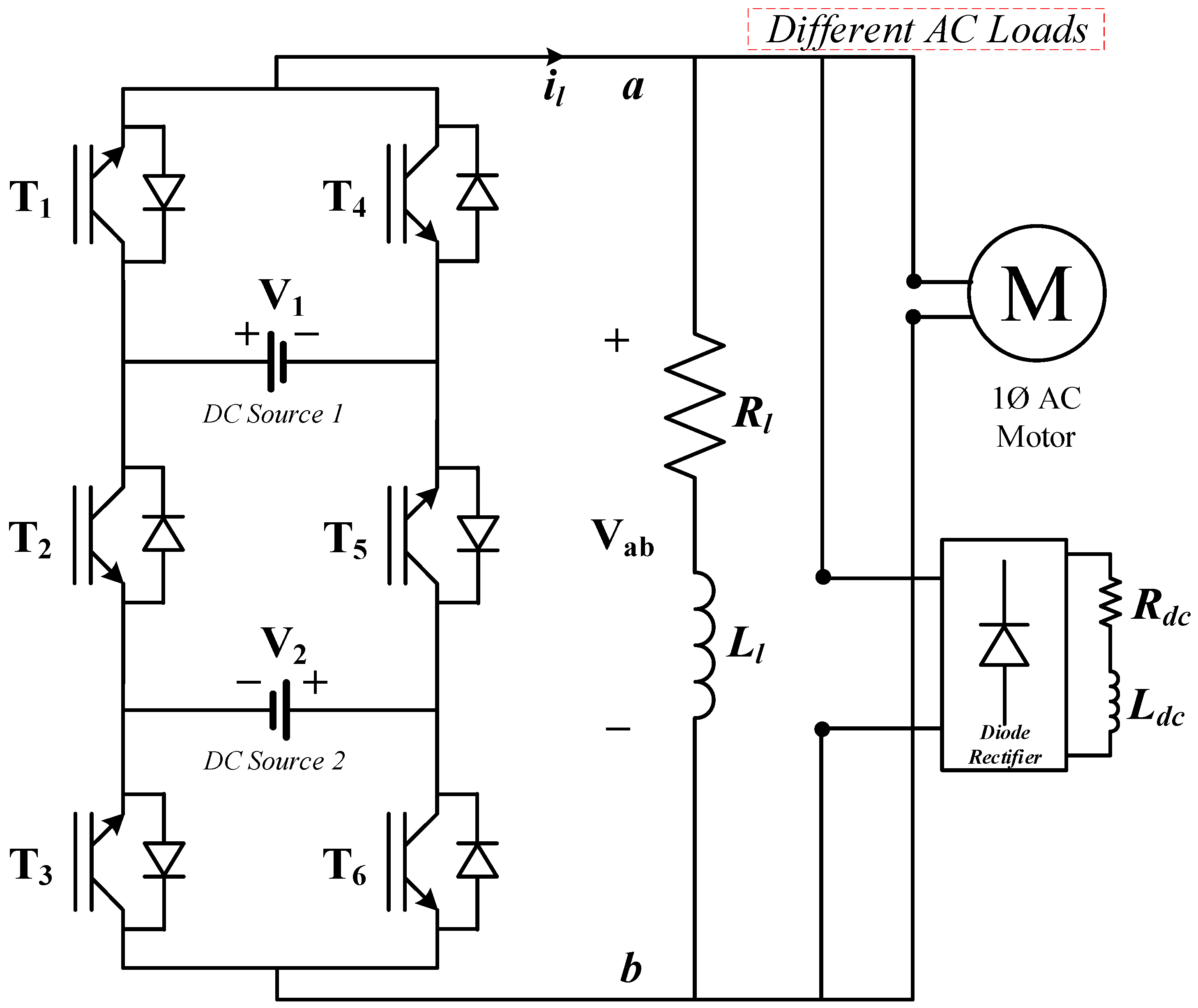
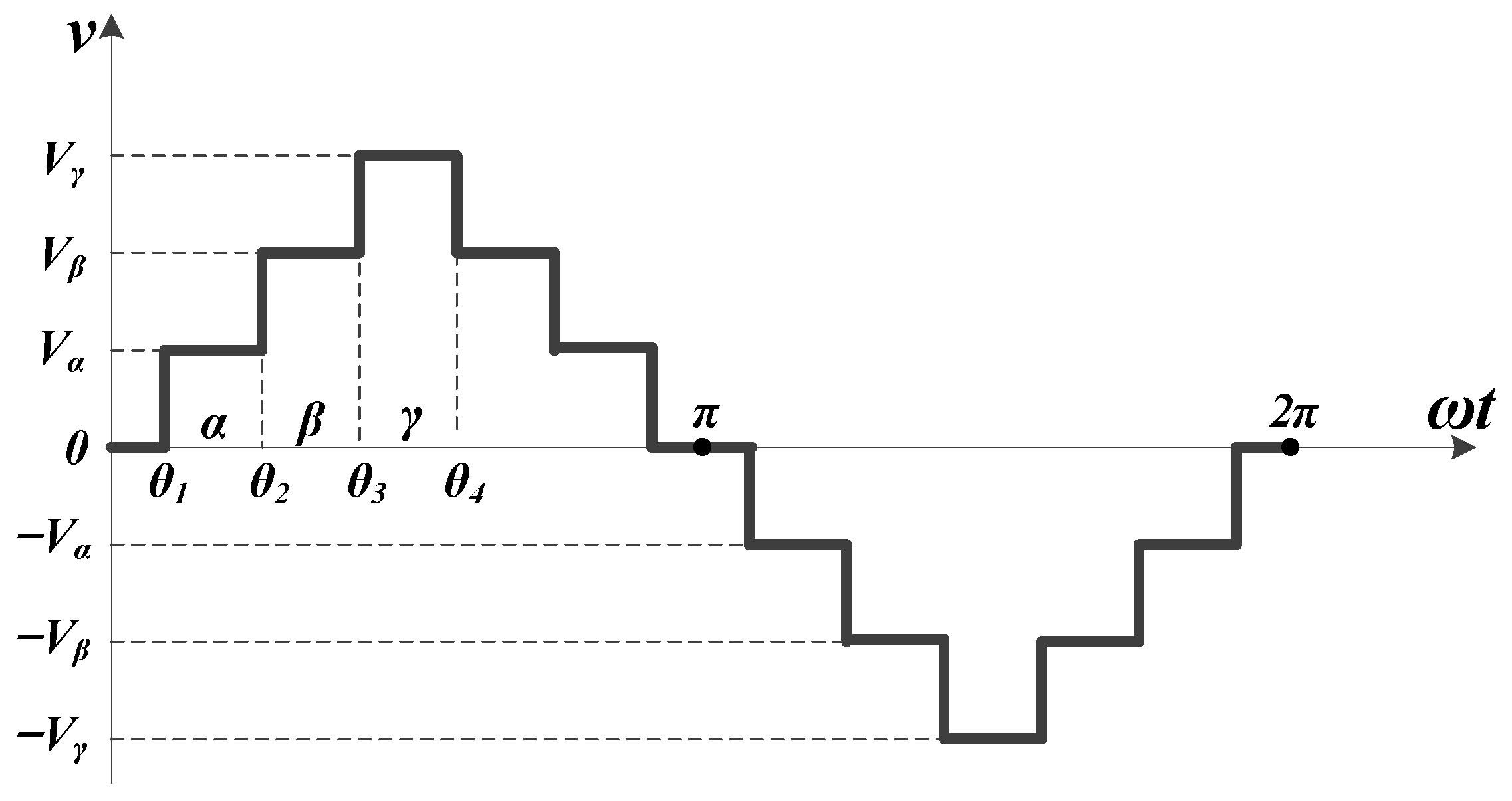
2. Seven-Level Modified Pack U-Cell Inverter

The seven-level MPUC inverter is shown in Figure 1. It has almost the same configuration as PUC5 but with a reversed direction of the lower DC source and two switches (T3 and T6). Unlike PUC5, which generates the maximum voltage level equal to its DC source [24], the MPUC inverter provides higher voltage amplitude by connecting two DC sources (V1 and V2) in series.
All possible switching states of the MPUC inverter are listed in Table 1. It is observed that if V1 is twice V2, then seven identical voltage levels will be produced at the output. Considering V1 = 2V2 = 2E, all seven voltage levels would be 0, ±E, ±2E, ±3E. The highest voltage level of 3E is generated by connecting two DC sources in series (V1 + V2). 2E is produced through the upper DC source (V1). The voltage level of E is sent to the output by the lower DC source (V2).
Paying attention to the switching states, it is clear that regardless of the switching and carrier frequency of PWM technique, T2 and T5 will work at the line frequency, which is 60 Hz in this work. This fact is proved through experimental results in the next sections. This helps to reduce the switching losses significantly. Moreover, having redundant states at 0 voltage helps reduce the switching frequency during the transition of the reference AC signal between positive and negative half cycles. Moreover, the modulation details have been provided in [23]. As a brief summary, a four-carrier level-shifted PWM has been used to modulate the reference signal and generate the switching pulses according to Table 1.

3. Design Consideration for Standalone Applications

An analysis has been performed in case of the stand-alone application of the MPUC inverter delivering energy to the single-phase loads.
Since a single-phase load needs a certain RMS voltage value (120 V 60 Hz or 220 V 50 Hz), the following analyses are done based on Figure 2 to achieve a general formula for RMS value calculation of a seven-level inverter’s output AC voltage waveforms.
The RMS value of each alternating function ise given by:
V r m s = 1 T 0 T v 2 ( t )   d t ,
in which T is the alternating period and v(t) is the alternating function, for which the RMS value would be Vrms.
Based on Figure 2, the seven-level output voltage waveform is a modified square wave with a period of 2π, which is symmetrical on two positive and negative half cycles. Thus, Equation (1) can be rewritten for a seven-level waveform with the specified angles and level amplitudes demonstrated in Figure 2 as follows:
V r m s = 1 T 0 T v 2 ( t )   d t = 1 2 π 0 2 π v 2 ( t )   d ω t = 1 2 π [ 4 θ 1 θ 2 V α 2   d ω t + 4 θ 2 θ 3 V β 2   d ω t + 2 θ 3 θ 4 V γ 2   d ω t ] = 1 2 π [ 4 α V α 2 + 4 β V β 2 + 2 γ V γ 2 ]
Considering the voltage values and levels in Table 1 for a seven-level MPUC inverter, the following formula will be derived for its output voltage RMS value:
V r m s = 1 2 π [ 4 α V 1 2 + 4 β V 2 2 + 2 γ ( V 1 + V 2 ) 2 ] = 1 2 π [ 4 α V 1 2 + 4 β ( 2 V 1 ) 2 + 2 γ ( 3 V 1 ) 2 ] = V 1 4 α + 16 β + 18 γ 2 π = V 1 2 α + 8 β + 9 γ π .
Consider that α, β, and γ are the angles at which the reference wave crosses the voltage levels as fixed lines between carriers. For instance, in a seven-level inverter, there are six carriers to modulate the reference waveform. Since they have been shifted vertically between +1 and −1, then each level line will have values of 2/3, 1/3, 0, −1/3, and −2/3, respectively. The reference wave function is assumed to be:
V r e f = m a sin ω t ,
where ma is the modulation index. As an example, α can be calculated by equaling the Vref function and the level line of 1/3, where the amplitude is V2 = E.
m a sin ω t = 1 3 α = ω t = arcsin 1 3 m a
By similar calculations, all other angles can be computed and substituted in Equation (3). Consequently, the RMS voltage value for the proposed seven-level MPUC inverter, in terms of output maximum voltage amplitude (Vmax = 3V2 = 3E) and modulation index, has been obtained voa the following formula:
V r m s = 0.725 × m a × V max .
As a single-phase stand-alone application in a 120 V 60 Hz grid, the output maximum voltage should be around 170 and the RMS value is 120 V. One possible case for DC source amplitudes and ma can be as follows:
{ V 1 = 113.2   V V 2 = 56.6   V m a = 0.98 .
That results in generating an output RMS value of 120 V and a maximum value of almost 170 V.
The other design consideration is described in the next section about the switching frequencies and voltage ratings of the switches using experimental test results.

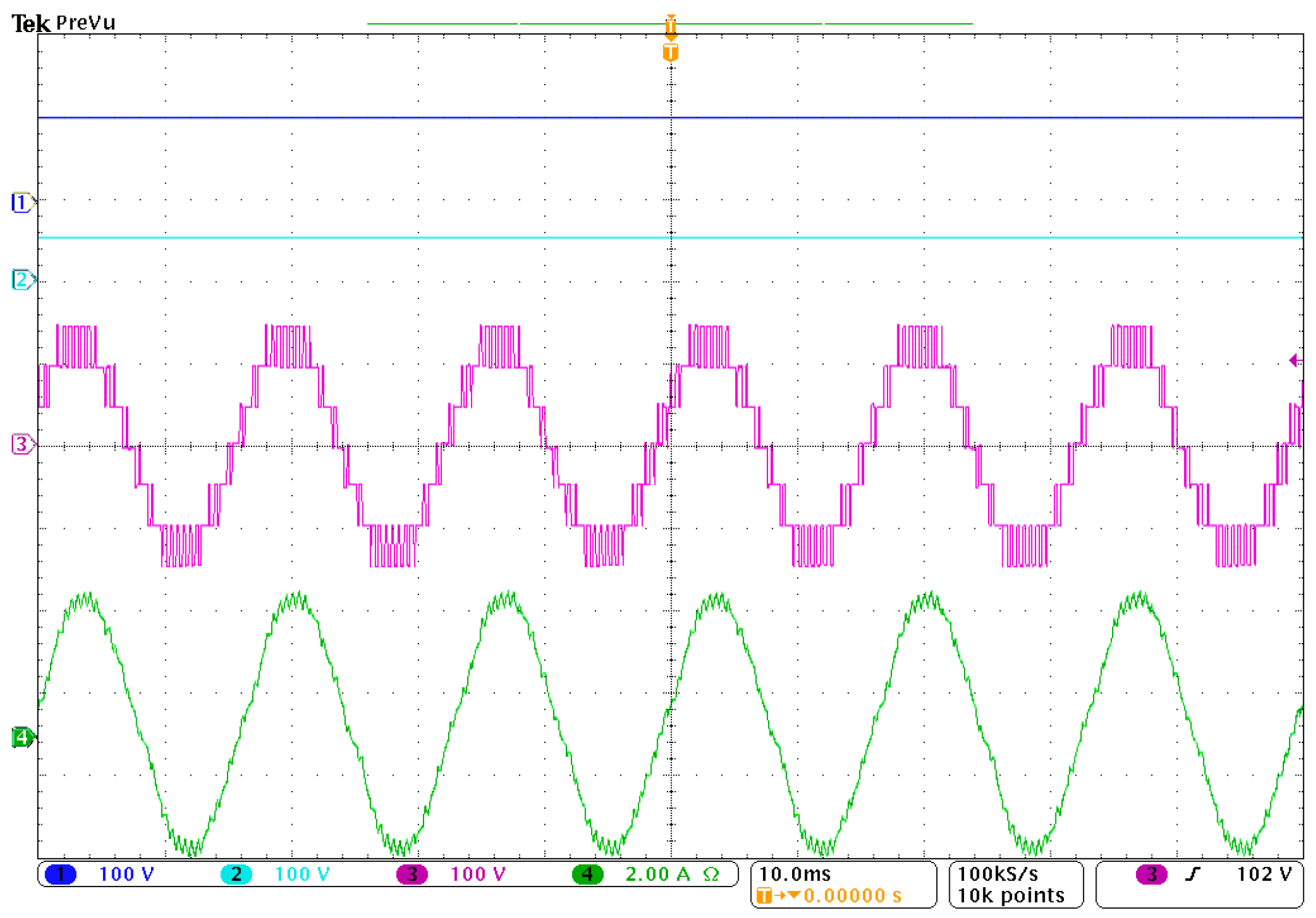
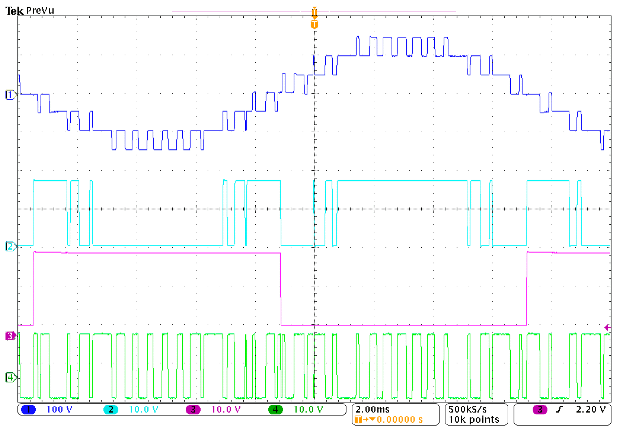
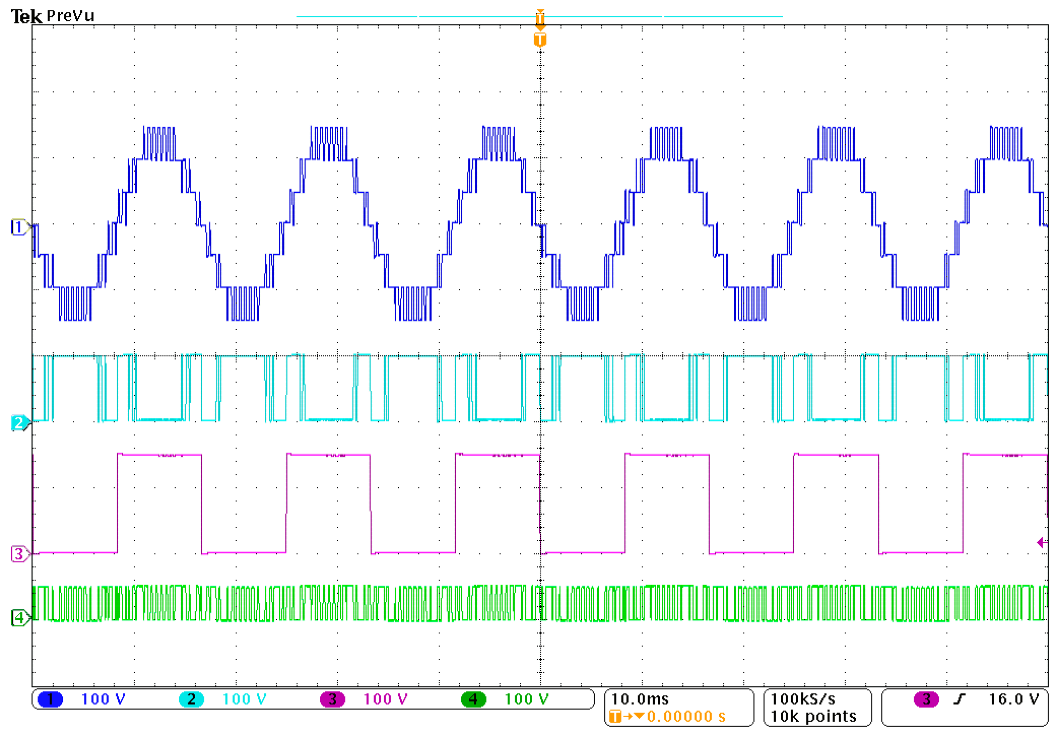
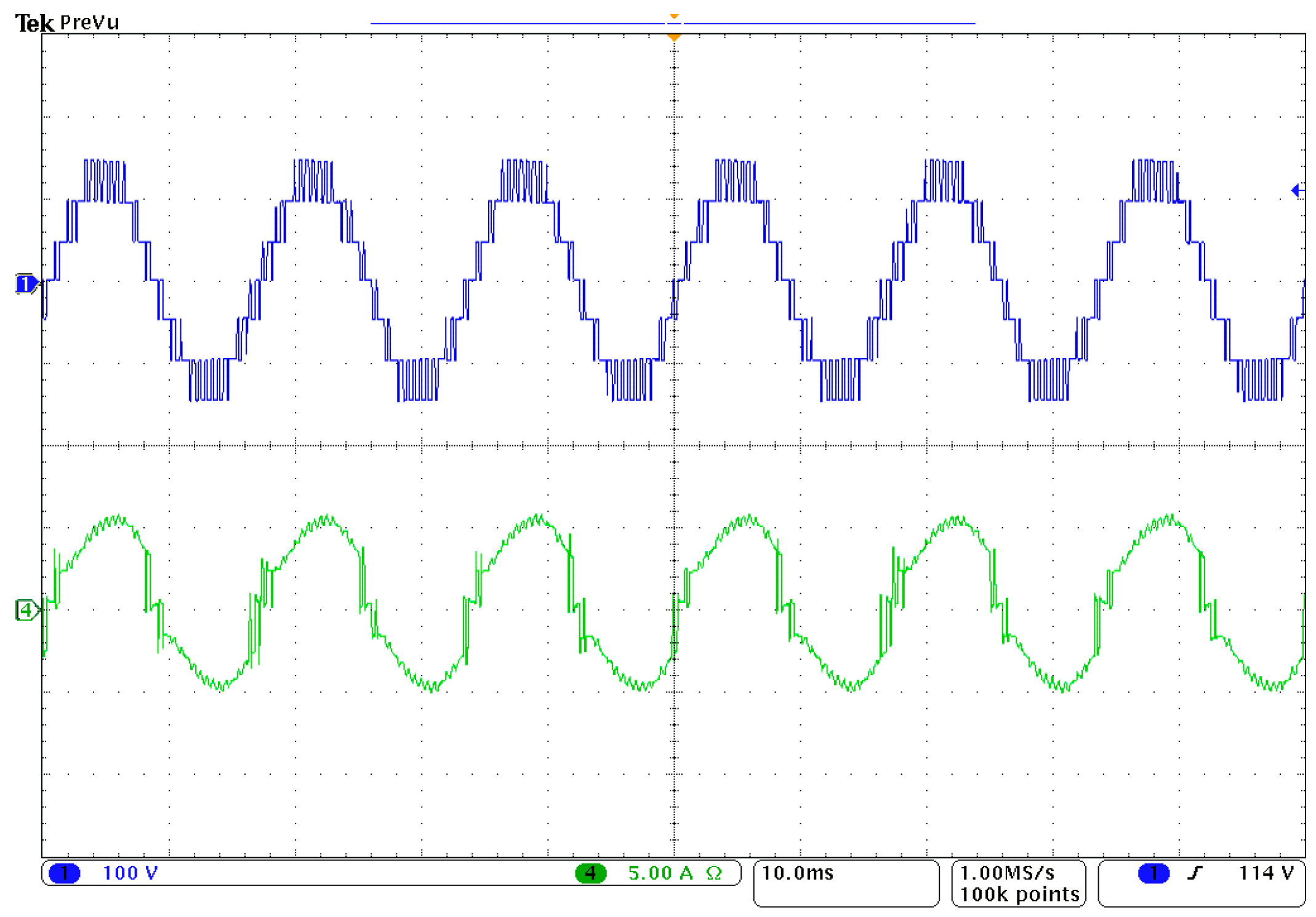
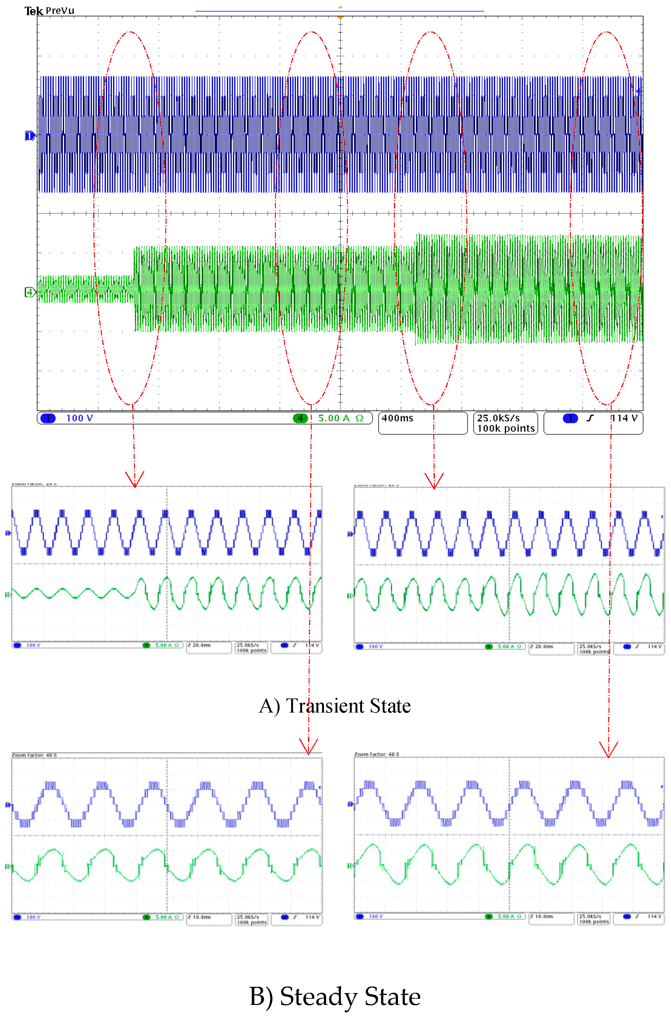
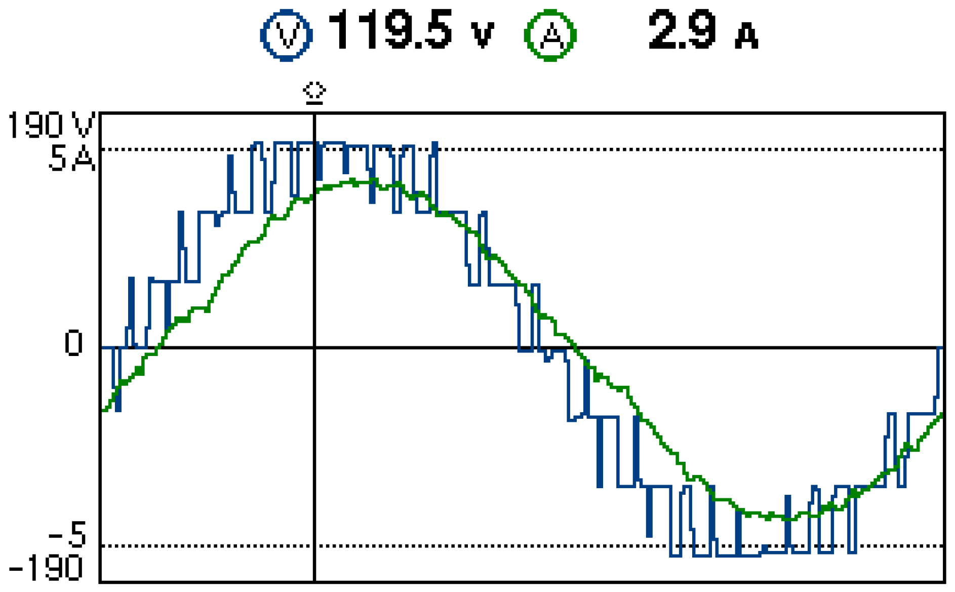
4. Experimental Results and Discussion

The proposed seven-level MPUC inverter has been implemented in standalone mode to verify the above analysis. It has been tested under various load types including linear and nonlinear. Six IGBT switches (600 V, 30 A, FGH30N60LSD) have been used in the experimental prototype. The designed switching algorithm was thoroughly explained in [23], which uses four level-shifted carriers to modulate the reference signal. It has been implemented on a dSpace 1103 real-time controller to generate switching pulses and fire the switches through gate drivers. Table 2 includes the complete system parameters. The whole setup was prepared based on Figure 1. Two DC sources are connected to the DC links V1 and V2 and different loads are connected at the output.
In the first test, the MPUC inverter has been connected to an RL load with parameters of Rl and Ll shown in Table 2 and the results are illustrated in Figure 3. The Vab waveform includes identical seven voltage levels with a maximum value of 150 V, which is the sum of two DC source amplitudes. The symmetrical load voltage and current waveforms prove the appropriate modulation technique. Moreover, the total harmonic distortion (THD) of the output voltage waveform without using any filters is 6%. With this low harmonic voltage, the required filters would be small and cost-effective for every application of the MPUC inverter, especially as a renewable energy interface.
To investigate the switching frequency of the MPUC topology, the gate pulses of switches T1, T2 and T3 as well as the output voltage have been captured for one cycle, which is illustrated in Figure 4. By counting the switching pulses in one cycle, the switching frequency of MPUC inverter IGBTs can be calculated, as presented in Table 3. Since each pair of switches is working complementarily, both switches in each cell would have an identical working frequency.
The voltage rating of each switch has been measured and the results are depicted in Figure 5. From Figure 4 and Figure 5, it is obvious that the two upper switches have a voltage rating of V1 and the two lower switches have to suffer the V2 during switching times. The advantage of the MPUC structure is that, although the two middle switches’ voltage ratings are higher than those of the other switches and it is V1 + V2, they are working at grid frequency, thus high-power switches with low switching frequency can be used in the middle cell including T2 and T5.
In another test, a nonlinear load including a single-phase diode rectifier with resistor and inductor on its DC side (Rdc = 20 Ω and Ldc = 60 mH) has been added, as shown in Figure 1. The load voltage and current waveforms, as well as the rectifier DC side voltage and current, have been depicted in Figure 6.
Another test has been performed to show the performance of the proposed topology in real conditions. In this part, the MPUC was supplying the RL load to which the nonlinear load was connected, and after a while a single-phase universal motor was paralleled with other loads (linear and nonlinear). The step-by-step process for connecting loads is depicted in Figure 7, which shows acceptable results in the case of UPS application.
For the last test, the design consideration explained in Section 3 regarding the 120 V output AC voltage RMS value has been applied. Figure 8 shows the output voltage and current waveforms as well as RMS values that are near the expected value calculated earlier in Equation (7). In this case, the source values have been set to 113.2 V and 56.6 V, respectively, and the ma is 0.98 to generate a voltage waveform with maximum 170 V and RMS value of 120 V 60 Hz useable for single-phase UPS applications.
Finally, a comparison has been performed between a single-phase MPUC inverter and the popular topology of multilevel inverters called Cascaded H-Bridge (CHB), which contains full-bridge inverter cells including four semiconductor switches and one DC source in each cell [25]. The CHB inverter can generate different voltage levels based on the connected DC sources’ amplitudes. If the DC sources are identical it would be called CHB with equal DC sources; if the sources are not identical, it is called CHB with unequal DC sources. Table 4 contains information to compare the seven-level MPUC inverter to the seven-level CHB inverters with equal and unequal DC sources.
As shown in Table 4, the advantage of the proposed seven-level MPUC inverter is that it has fewer components, which makes it cost-effective for manufacturers. Moreover, the low THD of the output voltage requires small filters that can make the inverter package smaller than other conventional inverters. Finally, it should be mentioned that the low switching frequency of the MPUC switches leads to reduced power losses that increase the inverter efficiency and lifetime.
As a simple comparison with CHB and NPC, it could be mentioned that the MPUC converter uses only six switches and two DC sources to generate a seven-level voltage waveform. In a similar case, the CHB uses eight switches that increase the manufacturing costs and power losses. Moreover, NPC uses 12 active switches, 10 diodes, and six DC sources to produce a seven-level voltage waveform that is obviously much more expensive and makes more power losses.
Moreover, looking at Figure 1, it can be seen that the two pairs of switches have common emitter (T2–T3, T4–T5), so their gate drives need a common power supply, which entails a reduction in the size of the manufactured circuit boards.

5. Conclusions

In this paper a reconfigured PUC inverter topology has been presented and studied experimentally. The proposed MPUC inverter can generate a seven-level voltage waveform at the output with low harmonic contents. The associated switching algorithm has been designed and implemented on the introduced MPUC topology with reduced switching frequency aspect. Switches’ frequencies and ratings have been investigated experimentally to validate the good dynamic performance of the proposed topology. Moreover, the comparison of MPUC to the CHB multilevel inverter showed other advantages of the proposed multilevel inverter topology, including fewer components, a lower manufacturing price, and a smaller package due to reduced filter size.

Author Contributions

All authors contributed equally to the work presented in this paper.

Funding

This research received no external funding.

Conflicts of Interest

The authors declare no conflict of interest.

References

  1. Bose, B.K. Multi-Level Converters; Multidisciplinary Digital Publishing Institute: Basel, Switzerland, 2015. [Google Scholar]
  2. Mobarrez, M.; Bhattacharya, S.; Fregosi, D. Implementation of distributed power balancing strategy with a layer of supervision in a low-voltage DC microgrid. In Proceedings of the 2017 IEEE Applied Power Electronics Conference and Exposition (APEC), Tampa, FL, USA, 26–30 March 2017; pp. 1248–1254. [Google Scholar]
  3. Franquelo, L.G.; Rodriguez, J.; Leon, J.I.; Kouro, S.; Portillo, R.; Prats, M.A.M. The age of multilevel converters arrives. IEEE Ind. Electron. Mag. 2008, 2, 28–39. [Google Scholar] [CrossRef]
  4. Malinowski, M.; Gopakumar, K.; Rodriguez, J.; Perez, M.A. A survey on cascaded multilevel inverters. IEEE Trans. Ind. Electron. 2010, 57, 2197–2206. [Google Scholar] [CrossRef]
  5. Nabae, A.; Takahashi, I.; Akagi, H. A new neutral-point-clamped PWM inverter. IEEE Trans. Ind. Appl. 1981, 5, 518–523. [Google Scholar] [CrossRef]
  6. Samadaei, E.; Gholamian, S.A.; Sheikholeslami, A.; Adabi, J. An Envelope Type (E-Type) Module: Asymmetric Multilevel Inverters with Reduced Components. IEEE Trans. Ind. Electron. 2016, 63, 7148–7156. [Google Scholar] [CrossRef]
  7. Babaei, E.; Gowgani, S.S. Hybrid multilevel inverter using switched capacitor units. IEEE Trans. Ind. Electron. 2014, 61, 4614–4621. [Google Scholar] [CrossRef]
  8. Vahedi, H.; Al-Haddad, K.; Ounejjar, Y.; Addoweesh, K. Crossover Switches Cell (CSC): A New Multilevel Inverter Topology with Maximum Voltage Levels and Minimum DC Sources. In Proceedings of the 39th Annual Conference of the IEEE Industrial Electronics Society, Vienna, Austria, 10–13 November 2013. [Google Scholar]
  9. Schweizer, M.; Kolar, J.W. Design and implementation of a highly efficient three-level T-type converter for low-voltage applications. IEEE Trans. Power Electron. 2013, 28, 899–907. [Google Scholar] [CrossRef]
  10. Escalante, F.M.; Vannier, J.C.; Arzandé, A. Flying capacitor multilevel inverters and DTC motor drive applications. IEEE Trans. Ind. Electron. 2002, 49, 809–815. [Google Scholar] [CrossRef]
  11. Trabelsi, M.; Bayhan, S.; Metry, M.; Abu-Rub, H.; Ben-Brahim, L.; Balog, R. An effective Model Predictive Control for grid connected Packed U Cells multilevel inverter. In Proceedings of the 2016 IEEE Power and Energy Conference at Illinois (PECI), Urbana, IL, USA, 19–20 February 2016. [Google Scholar]
  12. Zhang, C.; Geng, H.; Li, S.; Yang, G.; Dong, L. Hybrid Communication Topology and Protocol for Distributed-Controlled Cascaded H-Bridge Multilevel STATCOM. IEEE Trans. Ind. Appl. 2017, 53, 576–584. [Google Scholar]
  13. Gowaid, I.A.; Adam, G.P.; Massoud, A.M.; Ahmed, S.; Williams, B.W. Hybrid and Modular Multilevel Converter Designs for Isolated HVDC-DC Converters. IEEE J. Emerg. Sel. Top. Power Electron. 2018, 6, 188–202. [Google Scholar] [CrossRef]
  14. Vahedi, H.; Al-Haddad, K. PUC5 Inverter—A Promising Topology for Single-Phase and Three-Phase Applications. In Proceedings of the IECON 2016-42nd Annual Conference of the IEEE Industrial Electronics Society, Florence, Italy, 23–26 October 2016. [Google Scholar]
  15. Vahedi, H.; Kanaan, H.Y.; Al-Haddad, K. PUC converter review: Topology, control and applications. In Proceedings of the IECON 2015-41st Annual Conference of the IEEE Industrial Electronics Society, Yokohama, Japan, 9–12 November 2015; pp. 4334–4339. [Google Scholar]
  16. Kumar, P.R.; Kaarthik, R.S.; Gopakumar, K.; Leon, J.I.; Franquelo, L.G. Seventeen-level inverter formed by cascading flying capacitor and floating capacitor H-bridges. IEEE Trans. Power Electron. 2015, 30, 3471–3478. [Google Scholar] [CrossRef]
  17. Kumar, R.; Singh, B. Single Stage Solar PV Fed Brushless DC Motor Driven Water Pump. IEEE J. Emerg. Sel. Top. Power Electron. 2017, 5, 1377–1385. [Google Scholar] [CrossRef]
  18. Vahedi, H.; Labbe, P.; Al-Haddad, K. Sensor-Less Five-Level Packed U-Cell (PUC5) Inverter Operating in Stand-Alone and Grid-Connected Modes. IEEE Trans. Ind. Informat. 2016, 12, 361–370. [Google Scholar] [CrossRef]
  19. Vahedi, H.; Al-Haddad, K. Method and System for Operating a Multilevel Inverter. U.S. Patent US9923484B2, 20 March 2018. [Google Scholar]
  20. Sulake, N.; Devarasetty Venkata, A.; Choppavarapu, S. FPGA Implementation of a Three-Level Boost Converter-fed Seven-Level DC-Link Cascade H-Bridge inverter for Photovoltaic Applications. Electronics 2018, 7, 282. [Google Scholar] [CrossRef]
  21. Kang, J.-W.; Hyun, S.-W.; Ha, J.-O.; Won, C.-Y. Improved Neutral-Point Voltage-Shifting Strategy for Power Balancing in Cascaded NPC/H-Bridge Inverter. Electronics 2018, 7, 167. [Google Scholar] [CrossRef]
  22. Lee, S.; Kim, J. Optimized Modeling and Control Strategy of the Single-Phase Photovoltaic Grid-Connected Cascaded H-bridge Multilevel Inverter. Electronics 2018, 7, 207. [Google Scholar] [CrossRef]
  23. Vahedi, H.; Sharifzadeh, M.; Al-Haddad, K. Modified Seven-Level Pack U-Cell Inverter for Photovoltaic Applications. IEEE J. Emerg. Sel. Top. Power Electron. 2018, 6, 1508–1516. [Google Scholar] [CrossRef]
  24. Vahedi, H.; Al-Haddad, K. Real-Time Implementation of a Seven-Level Packed U-Cell Inverter with a Low-Switching-Frequency Voltage Regulator. IEEE Trans. Power Electron. 2016, 31, 5967–5973. [Google Scholar] [CrossRef]
  25. Wu, B. High-Power Converters and AC Drives; Wiley-IEEE Press: Hoboken, NJ, USA, 2006. [Google Scholar]
Figure 1. Single-phase seven-level MPUC inverter in standalone mode of operation.
Electronics 08 00268 g001
Figure 2. Seven-level AC waveform with specified angles for RMS calculation.
Electronics 08 00268 g002
Figure 3. Seven-level MPUC inverter output voltage and current with DC source voltages. Ch1: V1, Ch2: V2, Ch3: Vab, Ch4: il.
Electronics 08 00268 g003
Figure 4. One cycle of output voltage and gate pulses of MPUC inverter switches. Ch1: Vab, Ch2: T1 gate pulses, Ch3: T2 gate pulses, Ch4: T3 gate pulses.
Electronics 08 00268 g004
Figure 5. MPUC inverter switches’ voltage ratings. Ch1: Vab, Ch2: T1 voltage, Ch3: T2 voltage, Ch4: T3 voltage.
Electronics 08 00268 g005
Figure 6. Test results when a nonlinear load is connected to the MPUC inverter. Ch1: Vab, Ch4: il.
Electronics 08 00268 g006
Figure 7. Output voltage and current waveform of MPUC inverter when different loads are added step by step. Ch1: Vab, Ch4: il. (A) Transient state when nonlinear load is added to the RL load (left) and after a while a motor load is added to the system (right); (B) steady state when a nonlinear load is added to the RL load (left) and after a while a motor load is added to the system (right).
Electronics 08 00268 g007
Figure 8. Voltage and current waveform of MPUC inverter with RMS calculation for 120 V system.
Electronics 08 00268 g008
Table 1. All possible switching states and voltage levels of MPUC inverter.
Switching StateT1T2T3T4T5T6Vab
1101010V1 + V2
2100011V1
3001110V2
40001110
51110000
6110001−V2
7011100−V1
8010101V2 + V1
Table 2. Experimental setup parameters.
First DC bus voltage (V1)100 V
Second DC bus voltage (V2)50 V
Load Voltage Frequency (fgrid)60 Hz
Switching Frequency (fPWM)2 KHz
AC Load Resistor (Rl)40 Ω
AC Load Inductor (Ll)20 mH
Rectifier Side Resistor (Rdc)20 Ω
Rectifier Side Inductor (Ldc)60 mH
Single-Phase AC Universal Motor120 V, 3 A
Table 3. Switching frequency of MPUC inverter switches.
T1 & T4600 Hz
T2 & T560 Hz
T3 & T61920 Hz
Table 4. Comparison between seven-level MPUC topology and seven-level CHBs inverter.
TopologiesActive SwitchesDC Sources
seven-level CHB with Equal DC Sources123
seven-level CHB with Unequal DC Sources82
seven-level MPUC62

