Abstract
In this study, a split-gate resurf stepped oxide with a floating electrode (FSGRSO) UMOSFET has been proposed. The source in the trench is divided into two electrodes, namely: the upper electrode and the lower electrode. The upper one is the floating electrode, which redistributes the electric potential vertically, and improves the breakdown voltage and figure of merit (FOM). The breakdown (BV) and FOM of the FSGRSO UMOSFET have been improved up to 27.3% and 62.7%, respectively, compared with the SGRSO UMOSFET, according to the simulation results.
1. Introduction
With the development of power electronic systems, the power metal oxide semiconductor field effect transistor (MOSFET) device has become one of the irreplaceable important devices in the field of microelectronics because of its excellent performance. The breakdown (BV) and on-state specific resistance (RSP) are the two most important characteristics of power MOSFETs. The RSP determines the power dissipation of the device, but it is difficult to realize a low RSP for the determined BV due to the one-dimensional silicon limit. Super-junction (SJ) structures [1,2,3,4] in the drift region have been proposed in order to overcome it. The SJ can decrease the RSP effectively at a given BV. However, it is difficult to avoid the problem of doping interdiffusion in the production process. Therefore, a trench MOSFET with a new structure, the resurf stepped oxide (RSO) U-shape MOSFET(UMOSFET) [5,6,7,8,9,10], has been proposed to solve the problem between the BV and RSP. It is based on utilizing an electrode embedded within an oxide-coated deep trench as a part of the drift region [5]. Subsequently, a split-gate RSO (SGRSO) UMOSFET [11,12,13,14,15,16,17,18,19,20] with an isolated field-plate (FP) between the gate and drain has been proposed. Compared with the RSO UMOSFET and typical trench MOSFET, it exhibits relatively low switching losses. However, the field distribution in the drift region of this structure is not ideal compared with the SJ MOSFET, especially for breakdown voltages above 200 V [21]. Some new structures have been proposed in recent years, such as a split-gate UMOSFET with a linearly graded doping profile [11,22], slope-side oxygen [23], or p-pillar [14,16]. However, it is difficult to control the epitaxial doping in the actual process and produce a better slope-side oxygen or p-pillar. Therefore, research about the advanced SGRSO UMOSFET structure that adjusts the distribution of the electric potential vertically and improves the breakdown voltage without increasing the on-state specific resistance (RSP) is an urgent problem that needs to be solved.
In recent years, a double SGRSO (DSGRSO) UMOSFET has been proposed, which has double electrodes in the trench and the lower electrode is floating [24]. However, the effect of the process on the thickness of the dielectric layer is not considered. In this study, a split-gate resurf stepped oxide with a floating electrode (FSGRSO) UMOSFET, as well as its fabrication feasibility, have been proposed in order to improve the FOM of the device. The source in the trench is divided into two electrodes, namely: the upper electrode and the lower electrode—the upper electrode is floating, which is opposite to the DSGRSO [24]. The floating electrode can redistribute the equipotential vertically, and obtains a better characteristic. The BV and FOM have been improved compared with the SGRSO UMOSFET according to the simulation results.
2. Device Structure and Principles of Operation
A simplified cross-sectional view of the FSGRSO UMOSFET is shown in Figure 1a. Conventionally, the split-gate electrode within the oxide-coated trenches is tied to the source in order to achieve charge-coupling during operation in the blocking mode, as shown in Figure 1b. In this work, a SGRSO UMOSFET has been proposed. The two field plates are dividedly in contact, as follows: the lower field plate (E2) is in contact with the source electrode, and the upper field plate is floating. A thicker oxide serves as an isolation oxide between the floating and source electrodes.
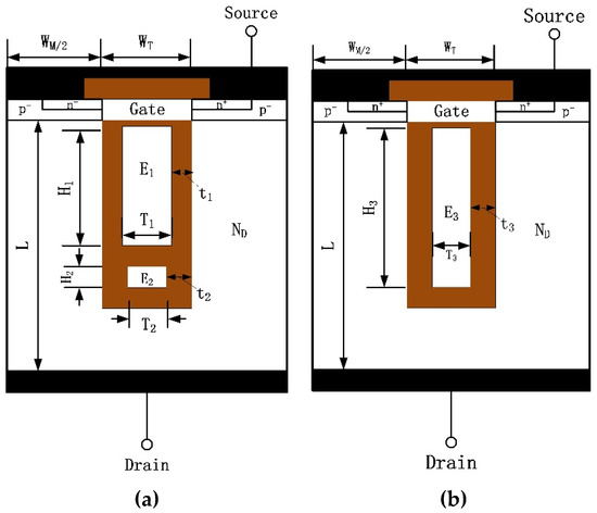
Figure 1.
Schematic cross-section of a (a) split-gate resurf stepped oxide with a floating electrode (FSGRSO)UMOSFETand a (b) split-gate resurf stepped oxide (SGRSO) UMOSFET.
The floating electrode can be regarded as an equipotential body in the electric field, and the surface of the floating electrode can be regarded as an equipotential surface. Therefore, the equipotential action of the floating electrode leads the high potential of the drain terminal to the source region with a low potential, and modulates the electric field of the drift region. It is similar to the resurf principle, which extends the depletion region to the entire drift region to reduce a high electric field at the surface of the source. As can be seen from Figure 2c,d, a portion of the dense potential lines at the bottom of the trench are transferred to the upper and middle area of the trench, and the potential lines are more evenly distributed in the drift region, because of the equipotential action of the floating electrode. In addition, the distribution of the electric field for the FSGRSO UMOSFET is more uniform than that of the SGRSO UMOSFET, as shown in Figure 2a,b. Therefore, the FSGRSO UMOSFET exhibits a higher BV and FOM.
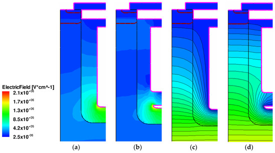
Figure 2.
Electric field distribution of the (a) SGRSO and (b) FSGRSO UMOSFETs, and the potential distribution of (c) the SGRSO and (d) FSGRSO UMOSFETs.
3. Fabrication Procedure
The process for the fabrication of the FSGRSO UMOSFET is similar to that of the basic SGRSO UMOSFET structure, as shown in Figure 3. This device structure was fabricated by starting with an n-type epitaxial layer grown on a heavily doped N+ substrate. Next, a deep trench was formed by reactive ion etching. Then, a thick oxide was thermally grown on the trench surface and etched off to smooth the trench corners (a). Next, a 1.2-μm oxide was deposited on the trench surface (b). The trench was then refilled with highly doped n-type polysilicon, and etched back to the depth (c). Afterward, the trench was refilled with oxide by depositing it again. All of the exposed oxide in the trench was removed, except for a thicker oxide, which served as an isolation oxide between the floating and the source electrodes (d). Subsequently, a thick oxide and n-type polysilicon were deposited again in the trench. The polysilicon was then etched until it was recessed below the surface to a depth slightly below the depth of the p-base region (e). Then, the thick oxide was etched back and a 50-nm oxide was thermally grown on the trench sidewalls to form the gate oxide (f). Following this, a third polysilicon layer was deposited and etched back to the surface to serve as the gate electrode (g). Finally, the p+ and n+ ions were implanted for the source region, and the device fabrication was then completed by the deposition of the source metal layer (h).
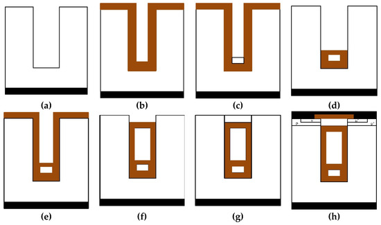
Figure 3.
Proposed fabrication process steps for the FSGRSO UMOSFET. (a) Trench are opend, (b) Thick oxide are deposited, (c) N-type Poly are deposited and etched back, (d) Trench are filled with oxide and etched back, (e) Thick oxide and N-type Poly are deposited, then the N-type Poly are etched back, (f) Gate oxide are grown, (g) Gate poly fills the trench and etch back, (h) Implante the p+ and n+ ions.
4. Results and Discussion
To compare the characters of the two structures, an extensive analysis of the device was conducted using the same structural parameters shown in Table 1. They were adopted from the model of bandgap narrowing, the concentration-dependent mobility model (CONMOB), the parallel electric field-dependent mobility model (FLDMOB), and the Shockley–Read–Hall model [24]. For the SGRSO UMOSFET, the target breakdown voltage was designed to be 200 V, using the details given in Table 1. The results show that the new structure device has better BV and FOM characteristics compared with the SGRSO UMOSFET.

Table 1.
Device parameters for the comparison of simulations.
Figure 4 shows the dependence of BV and FOM on the doping of the n-drift for the two structures. As the introduction of the floating electrode improved the distribution of the electric field in the n-drift, the BV and FOM (BV2/RSP) of the FSGRSO UMOSFET were higher than that of the SGRSO UMOSFET in a 4.7 × 10 to 9.4 × 10¹⁵/cm3 concentration. Furthermore, the gap of the breakdown voltage between the two structures’ devices gradually widened with the reduction of the epitaxial doping concentration in the range of a doping concentration of 4.7 × 10 to 6 × 10¹⁵/cm3. It achieved 258.3 and 202.9 V for the FSGRSO and SGRSO UMOSFETs, respectively, which was an improvement of 27.3%. Then, the FOM (BV2/RSP) of the FSGRSO UMOSFET improved by 62.7% compared with the SGRSO UMOSFET when the doping concentration was 6 × 10¹⁵/cm3.
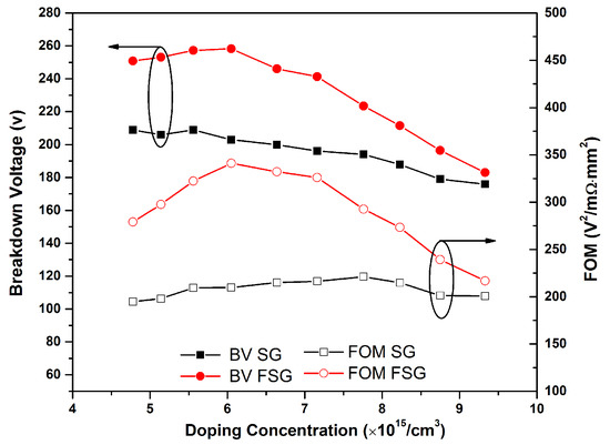
Figure 4.
Dependence of the breakdown (BV) and figure of merit (FOM) on the doping concentration.
Figure 5 gives the FSGRSO and SGRSO UMOSFETs’ dependence of BV or FOM on the mesa width (WM) when the doping concentration is 6.0 × 10¹⁵/cm3. The results show that the breakdown voltage and FOM values of the devices with a floating structure were always higher than those with an ordinary structure, in the range of 2.0 to 5.5 μm. Because of the modulating effect of the floating electrode, the electric field distribution in the drift area was more likely to be uniform. Therefore, the device with a floating structure could reach the optimal value with a small mesa width, which can reduce the cell pitch, the on–off resistance, and the power consumption, and increase the original cell density and the current with the same chip area. The devices with a floating electrode and ordinary structure reached the optimal value when the mesa width was 3.4 and 4.4 μm, respectively, as shown in Figure 5. The BV and FOM of the FSGRSO UMOSFET were improved by up to 27.3% and 62.7%, respectively, at a 3.4 μm mesa width.
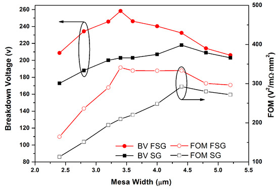
Figure 5.
Dependence of BV and FOM on the mesa width.
The dependence of the BV and FOM on the thickness of the drift region (L) is shown in Figure 6 at a 3.4-μm mesa width for the two structures. The results show that the trends of the BV and FOM, depending on the thickness of the drift region, were similar for the FSGRSO and SGRSO UMOSFETs. Furthermore, the BV and FOM (BV2/Rsp) of the FSGRSO UMOSFET were higher than that of the SGRSO UMOSFET in 10–25 μm, due to the floating electrode. The breakdown voltage of the two devices rose and stabilized gradually with the increase of the drift region thickness. However, the FOM value decreased as the L increased above 16 μm, and achieved a maximum value when the L was 16 μm, because of the increase of RSP with the drift region thickness. Its optimum FOM and BV improved by 66.8% and 29.7%, respectively, compared with that of the SGRSO UMOSFET when the L was 16 μm, as shown in Figure 6.
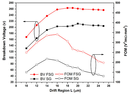
Figure 6.
Dependence of BV and FOM on the drift region thickness.
The relationship between the structure sizes of the FSGRSO UMOSFET and the BV is shown in Figure 7. The different values of the height (H1) and width (T1) for a floating electrode and the width of the source in the trench were considered. The effect of the equipotential gradually strengthen and the dense potential at the groove bottom gradually moved to the upper part with the increase of height in the floating electrode. Therefore, the BV of the FSGRSO UMOSFET was still higher than a device with ordinary construction. The BV of the FSGRSO UMOSFET achieved an optimal BV when H1 was 5.2 μm, which means that the potential line of the drift region reached an optimum state. If the length of the floating electrode was continuously increased or decreased, the balance would be broken and the breakdown voltage would decrease at the same time. The neighboring oxide thickness decreased with the increase of T2, which must be sufficient in order to provide the desired charge coupling and support the entire drain-blocking voltage. The result shows that the BV achieved an optimal value when the T2 and the oxide thickness were both 1.2 μm. The principle was the same as T1. To compare the characteristics of the FSGRSO and SGRSO UMOSFETs, we adopted the FOMs of BV2/RSP and RSP × Qgd. Figure 8 shows that the FOM (RSP × Qgd) of the FSGRSO UMOSFET is slightly higher compared with the SGRSO UMOSFET, because of the floating electrode, E1, which requires more research in the future.
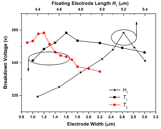
Figure 7.
Dependence of the BV on the width of the floating electrode E1 (T1), width of the floating electrode E2 (T2), and length of the floating electrode (H1) for the FSGRSO UMOSFET.
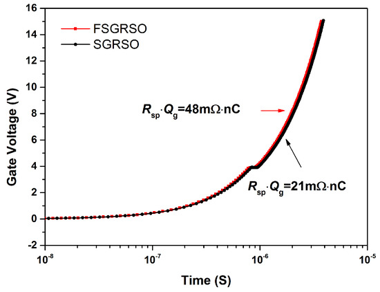
Figure 8.
FOM (on-state specific resistance (RSP) × Qgd) for the FSGRSO and SGRSO UMOSFETs.
Figure 9a shows the output characteristics for the SGRSO and FSGRSO UMOSFET for all of the bias conditions when the BV is 200 V, as shown in Figure 9b. The Rsp of the device is the ratio of the applied VDS to the resulting IDS in the linear region of the operation, multiplied by the active area, and it varies with the applied VGS [25]. It is obvious that the FSGRSO UMOSFET had a higher drain current compared with the conventional structure when the VGS was 4, 6, 8, and 12 V, respectively. When the VGS was 6 V, the current of the FSGRSO UMOSFET even exceeded the current of the SGRSO UMOSFET, at 12 V in particular. The Rsp evaluated at VDS = 0.3 V, as a function of the gate voltage for the FSGRSO UMOSFET in contrast to the SGRSO UMOSFET, is shown in Figure 9c. The FSGRSO UMOSFET decreased the Rsp by more than 15% compared with the SGRSO UMOSFET. Furthermore, the FSGRSO UMOSFET had a better transfer characteristic at VDS = 0.3 V, as shown in Figure 9d, because the floating electrode could modulate the electric field in the drift region of the device and improve the breakdown voltage of the device. Therefore, a device with a floating electrode structure can increase the doping concentration of the drift region and reduce the resistance at a given breakdown voltage. The characters of the proposed structure have been compared with the one-dimensional silicon limit and other UMOSFETs in Figure 10. We can see that the proposed device has a better performance over the previous power UMOSFET.
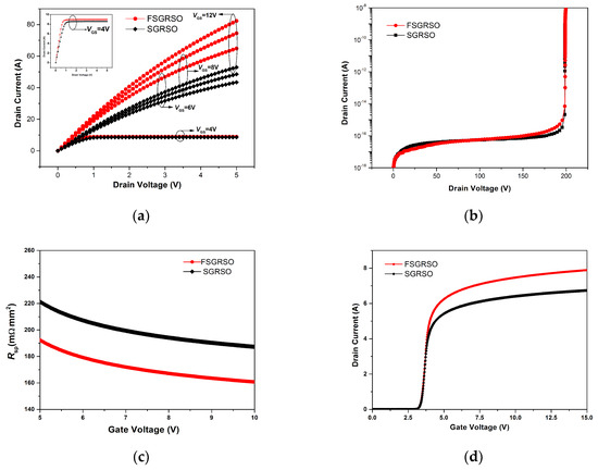
Figure 9.
Characteristics comparing of the SGRSO and FSGRSO UMOSFET (a) output characteristics at VGS = 12, 8, 6, and 4 V (inset); (b) breakdown voltage; (c) ON-state resistance (Rsp); and (d) transfer characteristic.
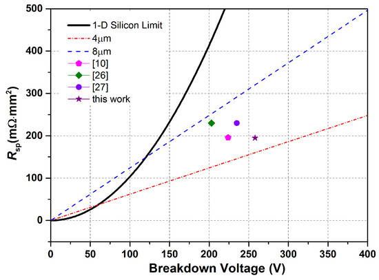
Figure 10.
RSP as a function of the BV for the one-dimensional silicon limit, two-dimensional charge-coupling limits for the pitches of 4 and 8 μm, references [10,26,27], and this work.
5. Conclusions
In this work, the FSGRSO UMOSFET has been proposed and verified, which has 258.3 V BV, 195 mΩ∙mm2 RSP, and 341 V2/ mΩ∙mm2 FOM. The source in the trench is divided into two electrodes, namely: the upper electrode and the lower electrode. The upper one is a floating electrode, which redistributes the electric potential vertically and improves the BV and FOM. The BV and FOM of FSGRSO UMOSFET have been improved up to 27.3% and 62.7%, respectively, according to the simulation results.
Author Contributions
Conceptualization, R.C. and L.W.; methodology, L.W.; software, N.J.; validation, N.J., H.Z. and M.G.; formal analysis, R.C.; investigation, R.C.; resources, L.W.; data curation, R.C.; writing—original draft preparation, R.C.; writing—review and editing, R.C.; visualization, N.J.; supervision, L.W.; project administration, L.W.; funding acquisition, L.W.
Funding
This research received no external funding.
Conflicts of Interest
The authors declare no conflict of interest.
References
- Lin, Z.; Huang, H.; Chen, X. An Improved Superjunction Structure with Variation Vertical Doping Profile. IEEE Trans. Electron Devices 2015, 62, 228–231. [Google Scholar] [CrossRef]
- Cao, Z.; Duan, B.; Shi, T.; Yuan, S.; Yang, Y. A Superjunction U-MOSFET with SIPOS Pillar Breaking Superjunction Silicon Limit by TCAD Simulation Study. IEEE Electron Device Lett. 2017, 38, 794–797. [Google Scholar] [CrossRef]
- Park, J.; Lee, J. A 650 V Super-Junction MOSFET with Novel Hexagonal Structure for Superior Static Performance and High BV Resilience to Charge Imbalance: A TCAD Simulation Study. IEEE Electron Device Lett. 2017, 38, 111–114. [Google Scholar] [CrossRef]
- Kang, H.; Udrea, F. Analytic Model of Specific ON-State Resistance for Superjunction MOSFETs with an Oxide Pillar. IEEE Electron Device Lett. 2019, 40, 761–764. [Google Scholar] [CrossRef]
- Baliga, B.J. Vertical Field Effect Transistors Having Improved Breakdown Voltage Capability and Low On-State Resistance. U.S. Patent 5637898A, 10 June 1997. [Google Scholar]
- Koops, G.E.J.; Hijzen, E.A.; Hueting, R.J.E.; Zandt, M.A.A. RESURF stepped oxide (RSO) MOSFET for 85V having a record-low specific on-resistance. In Proceedings of the 16th International Symposium on Power Semiconductor Devices and ICs, Kitakyushu, Japan, 24–27 May 2004; pp. 185–188. [Google Scholar]
- Gajda, M.A.; Hodgskiss, S.W.; Mounfield, L.A.; Irwin, N.T.; Koops, G.E.J.; van Dalen, R. Industrialisation of Resurf Stepped Oxide Technology for Power Transistors. In Proceedings of the IEEE International Symposium on Power Semiconductor Devices and IC’s, Naples, Italy, 4–8 June 2006; pp. 1–4. [Google Scholar]
- Goarin, P.; Koops, G.E.J.; van Dalen, R.; Cam, C.L.; Saby, J. Split-gate Resurf Stepped Oxide (RSO) MOSFETs for 25V applications with record low gate-to-drain charge. In Proceedings of the 19th International Symposium on Power Semiconductor Devices and IC’s, Jeju Island, Korea, 27–31 May 2007; pp. 61–64. [Google Scholar]
- Tong, C.F.; Cortes, I.; Mawby, P.A.; Covington, J.A. Static and Dynamic Analysis of Split-Gate RESURF Stepped Oxide (RSO) MOSFETs for 35 V Applications. In Proceedings of the Conference on Electron Devices, Santiago de Compostela, Spain, 11–13 February 2009. [Google Scholar]
- Park, C.; Azam, M.; Dengel, G.; Shibib, A.; Terrill, K. A New 200 V Dual Trench MOSFET With Stepped Oxide for Ultra Low RDS(on). In Proceedings of the 31st International Symposium on Power Semiconductor Devices and ICs, Shanghai, China, 19–23 May 2019; pp. 95–98. [Google Scholar]
- Baliga, B.J.; North Carolina State University. Power Semiconductor Devices Having Improved High Frequency Switching and Breakdown Characteristics. U.S. Patent 5,998,833, 7 December 1999. [Google Scholar]
- Wang, Y.; Hu, H.; Jiao, W. Split-Gate-Enhanced UMOSFET with an Optimized Layout of Trench Surrounding Mesa. IEEE Trans. Electron Devices 2012, 59, 3037–3041. [Google Scholar] [CrossRef]
- Wang, Y.; Lan, H.; Cao, F.; Liu, Y.-T.; Shao, L. A novel power UMOSFET with a variable K dielectric layer. Chin. Phys. Soc. 2012, 21, 569–572. [Google Scholar]
- Wang, Y.; Hu, H.F.; Yu, C.H.; Lan, H. High-performance split-gate enhanced UMOSFET with p-pillar structure. IEEE Trans. Electron Devices 2013, 60, 2302–2307. [Google Scholar] [CrossRef]
- Wang, Y.; Lan, H.; Dou, Z.; Hu, H.F. Method to improve trade-off performance for split-gate power U-shape metal-oxide semiconductor field-effect transistor with compound trench dielectrics. IET Power Electron. 2014, 7, 2030–2034. [Google Scholar]
- Wang, Y.; Hu, H.F.; Wang, L.G.; Yu, C.H. Split gate resurf stepped oxide UMOSFET with P-pillar for improved performance. IET Power Electron. 2014, 7, 965–972. [Google Scholar] [CrossRef]
- Wang, Y.; Hu, H.F.; Yu, C.-H.; Wei, J.-T. Advanced hexagonal layout design for split-gate reduced surface field stepped oxide U-groove metal–oxide–semiconductor field-effect transistor. IET Power Electron. 2015, 8, 678–684. [Google Scholar]
- Park, C.; Havanur, S.; Shibib, A.; Terrill, K. 60 V rating split gate trench MOSFETs having best-in-class specific resistance and figure-of-merit. In Proceedings of the 28th International Symposium on Power Semiconductor Devices and ICs, Prague, Czech Republic, 12–16 June 2016; pp. 387–390. [Google Scholar]
- Wang, Y.; Yu, C.; Li, M.; Cao, F.; Liu, Y. High-Performance Split-Gate-Enhanced UMOSFET with Dual Channels. IEEE Trans. Electron Devices 2017, 64, 1455–1460. [Google Scholar] [CrossRef]
- Kobayashi, K.; Kato, H.; Nishiguchi, T.; Shimomura, S.; Ohno, T.; Nishiwaki, T.; Aida, K.; Ichinoseki, K.; Oasa, K.; Kawaguchi, Y. 100-V Class Two-step-oxide Field-Plate Trench MOSFET to Achieve Optimum RESURF Effect and Ultralow On-resistance. In Proceedings of the 31st International Symposium on Power Semiconductor Devices and ICs, Shanghai, China, 19–23 May 2019; pp. 99–102. [Google Scholar]
- Baliga, B.J. Advanced Power MOSFET Concepts; Springer Science and Business Media: New York, NY, USA, 2010. [Google Scholar]
- Baliga, B.J. Trends in power discrete devices. In Proceedings of the 10th International Symposium on Power Semiconductor Devices and ICs, Kyoto, Japan, 3–6 June 1998; pp. 5–10. [Google Scholar]
- Wang, Y.; Hu, H.; Jiao, W. High-Performance Gate-Enhanced Power UMOSFET with Optimized Structure. IEEE Electron Device Lett. 2010, 31, 1281–1283. [Google Scholar] [CrossRef]
- Wang, Y.; Hu, H.F.; Dou, Z.; Yu, C.H. Way of operation to improve performance for advanced split-gate resurf stepped oxide UMOS. IET Power Electron. 2014, 7, 2964–2968. [Google Scholar] [CrossRef]
- Shenai, K. A 55-V, 0.2-mΩ cm2 vertical trench power MOSFET. IEEE Electron Device Lett. 1991, 12, 108–110. [Google Scholar] [CrossRef]
- Hattori, Y.; Nakashima, K.; Kuwahara, M.; Yoshida, T.; Yamauchi, S.; Yamaguchi, H. Design of a 200V Super Junction MOSFET with n-buffer regions and its Fabrication by Trench Filling. In Proceedings of the International Symposium on Power Semiconductor Devices and ICs, Kitakyushu, Japan, 24–27 May 2004; pp. 189–192. [Google Scholar]
- Shibata, T.; Noda, Y.; Yamauchi, S.; Nogami, S.; Yamaoka, T.; Hattori, Y.; Yamaguchi, H. 200V Trench Filling Type Super Junction MOSFET with Orthogonal Gate Structure. In Proceedings of the 19th International Symposium on Power Semiconductor Devices and IC’s, Jeju Island, Korea, 27–31 May 2007; pp. 37–40. [Google Scholar]
© 2019 by the authors. Licensee MDPI, Basel, Switzerland. This article is an open access article distributed under the terms and conditions of the Creative Commons Attribution (CC BY) license (http://creativecommons.org/licenses/by/4.0/).