1. Introduction
Nowadays, there is no doubt that tests and debugging are crucial in electronics. These tests avoid damage to the hardware and allow engineers to know the behavior of the converter before including it in the real system. In recent years, due to the increase of digital controllers, a final system usually contains both digital and analog signals. In order to be able to work with these, different debugging techniques have emerged [
1,
2,
3]. One of the most important is hardware-in-the-loop (HIL), which allows debugging part of the system, such as the power converters, accurately emulating the behavior of the final real system and saving time, money, and effort during the design process [
4,
5,
6,
7,
8,
9,
10]. Recently, given the progress in digital electronics, the maximum switching frequencies that can be emulated in HIL have increased from tens to hundreds of kilohertz. The hardware platforms that can reach these real-time emulations are the field programmable gate arrays (FPGAs) [
11,
12,
13]. As such, in the last years the use of FPGAs with HIL models has increased [
14,
15,
16,
17,
18,
19].
In these real-time emulations of FPGAs, special attention must be paid to the occupied area and the integration step. To reach high switching frequency, a very small integration step is needed, however resolution problems can appear. Therefore, for both resolution issues and the final area in our design, the number representation in the signals plays a very important role. As has been previously studied by Sanchez et al. [
20], the fixed-point method is the perfect number representation method to optimize the integration step and area, due to the possibility of adjusting the number of bits for every signal, although this implies a higher time design than in the floating-point method [
18,
21,
22]. Sanchez et al. made a comparison among different representation methods, namely float-type and fixed-point methods, implementing a HIL model for a digital converter. They concluded that float can be synthesized, but this requires many resources. However, the fixed-point method is proposed as an alternative to this problem, because although it has the disadvantage of high design effort owing to the model being hand-coded, it also has an advantage in that every signal can be personalized regarding the number of bits, providing the minimum necessary number of bits without wasting them. Goñi et al. [
23] studied two methods to determine the number of bits of state variables in models of power converters and also in fixed-point simulated and analytical representation. However, the width of the other variables was not addressed. A similar analytical approach is used in this work for feedback signals. To our knowledge, no previous work has studied the influence of the number of bits of these signals, which play an important role in a power converter because it is a loop system and each signal influences the others. These signals transmit the value of one state variable to the rest of the system, which is required for the system to calculate the new value of the other state variables. This paper proposes to find out the minimum necessary number of bits for use in the feedback signals, the knowledge of which would increase the necessary resources for implementation. The information will be maintained to calculate a new and accurate value of the state variable in the next clock cycle.
The rest of the paper is organized as follows.
Section 2 presents the application example.
Section 3 presents the resolution issues, such as QX.Y notation and methods for estimation of the number of bits in the signals for implementation.
Section 4 presents the results. Finally,
Section 5 discusses the results and proposes a final design method, while conclusions are given in
Section 6.
2. Application Example
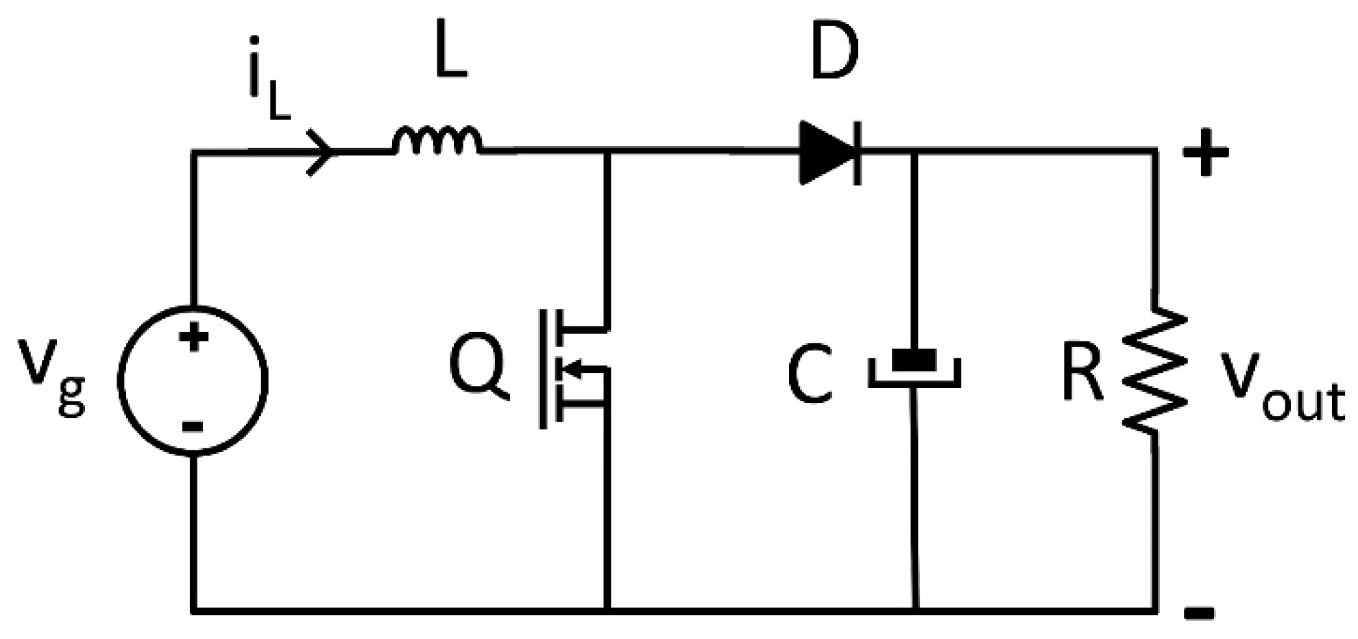
For the purpose of this paper, an application example is used, specifically a boost converter, to explain every process in detail. The topology of the boost converter is shown in
Figure 1. For the sake of clarity, the proposed model is the simplest one and does not contain losses, but similar conclusions could be drawn for other topologies. The model needs to calculate the state variables, namely the capacitor voltage (
vout) and the inductor current (
iL) in every time step considering the state of the switch.
The inductor voltage is defined by Equation (1)
From Equation (1), the inductor current for each time step
k, using the explicit Euler method, is defined as:
Similarly, the capacitor current is defined by Equation (3)
where, the output voltage for each time step
k is
where ∆
t is the simulation time step,
L is the inductance, and
C the capacitance. Considering the state of the switch (named
Q), the values of the inductor voltage (
vL) or capacitor current (
iC) change. When the switch is closed (
Q = 1), the diode does not conduct. On the one hand, the inductor current flows through the switch, while on the other hand the capacitor discharges through the load resistor. When the switch is open (
Q = 0) and the input current is positive, the diode conducts. This mode is known as continuous conduction mode (CCM). When the input current is zero and the diode does not conduct, the discontinuous conduction mode (DCM) appears. Thus, there are three possibilities: closed switch (
Q = 1), open switch (
Q = 0) in CCM when
iL > 0, and open switch in DCM when
iL = 0), which are defined in Equations (5), (6), and (7), respectively,
where
vg is the input voltage and
iR is the output current. The selected parameters of the boost converter used for experimental results are shown in
Table 1.
3. Resolution Issues and Implementation
This section describes the methods and rules that are applied to calculate the number of bits in the signals of our application example boost power converter.
The number of bits in the signals in HIL models of power converters is hugely important in real-time simulations in FPGAs. The clock frequency and the final area occupied in the FPGA are key factors in this kind of simulation. Although there are not many studies on the resolution of signals in HIL models of power converters, Goñi et al. [
23] proposed two methods to determine the resolution of state variables in models of power converters: an analytical approach and an approach based on simulations. Both methods lead to almost identical results, so the analytical approach is recommended due to its greatly reduced burden.
In the analytical approach, the width required for a state variable is determined by the maximum magnitude that can be stored in it (
x) and its resolution (∆
x). For state variables of power converters, which are the voltages in every capacitor and the currents in every inductor, it should be considered that the resolution for these signals is determined by their incremental values, which are added in every time step (see Equations (2) and (4)). Therefore, the width is determined by both the maximum and the incremental values. To be able to simultaneously represent both
x and ∆
x, the minimum number of bits would be:
However, ∆
x is only represented in Equation (8) by one bit, which is not enough to distinguish between its different values. For instance, with
x = 5 and ∆
x = 0.25, the width is 5 bits—three representing
x and two representing ∆
x. With this number of bits, in the fractional parts, only multiples of ∆
x can be represented, namely 0.25, 0.5, or 0.75. Then, as it has been previously shown in [
23] for the state variables, to be able to have enough resolution to store incremental values with higher accuracy, extra bits, named as
n, are added to the signal width:
Goñi et al. proposed that x should be the maximum value allowed in the simulation during transients, whereas ∆x is the minimum reasonable incremental value of the state variable excluding zero. For the value of n, they proposed that with a value around 8, the resolution obtained for the incremental values is enough. Following this approach, the number of bits for the state variables iL and vOut are obtained, as will be shown later.
Another important issue is the type of representation. In this paper, the fixed-point method with QX.Y notation has been chosen. With this notation, the number of bits for the integer part is named X, whereas the number of bits for the fractional part is named Y. Also, an extra bit denotes the sign using a complementary notation for 2. For instance, a Q5.2 signal has 1 + 5 + 2 bits. So, to represent 1.75 with this format, “00001” is used for X, with an inherent sign in the complementary notation of 2, while “11” is represented by Y, so finally the value is “0000111”. When the widths of the state variables are calculated with Equation (9), X has the number of bits needed to represent the maximum of the signal, and the rest are assigned to the fractional part Y. In other signals in the application, their widths depend on their associated hardware; therefore, they also depend on their equations. Rules of addition, subtraction, and multiplication with the fixed-point method are applied in order to retain information. To avoid overflow, in the addition and subtraction, the maximum of the integer parts of both operands (
X1 and
X2) is chosen by adding an extra bit. In the case of multiplication, the total number of bits of the integer part is the addition of the integer parts of both operands and an extra bit (
X1 +
X2 + 1). To avoid loss of resolution, the addition and subtraction requires the maximum of the fractional parts in the operands (
Y1 and
Y2), and in the case of multiplication requires the addition of both parts (
Y1 +
Y2).
For the implementation, the number of bits for every signal in the boost converter should be selected. Firstly, the signals, which are shown in
Figure 2, have to be classified. The state variables (
iL and
vout), constants (
dtL and
dtC), inputs (
vg and
ir), outputs (i
in and
voutExt), and feedback signals (
voutFeedback and
iLFeedback) are shown in red.
The state variables acquire their values from the addition of themselves and their incremental values, as is observed in Equations (2) and (4). As these variables are accumulative, the number of bits for their width, applying the rule of addition in the QX.Y notation (Equation (10)), would increase indefinitely. To avoid this, the width is limited to the value recommended by Goñi et al. in the analytical approach, shown in Equation (9). The maximum value during the transient phase for the output voltage, vout, is 792.7 V in the worst case simulation, whereas its increment is 20 µV. As such, the recommended width when applying Equation (9) is 26 + n (i.e., 34), but with the sign bit the total number of bits is 35. For the integer part (X), at least 10 bits are needed, with which the fractional part (Y) would be 24. Although 10 bits are enough for this specific maximum, to cover other possible critical maximums in other simulations, an extra bit is added to the integer part. Thus, the final format is Q (10 + 1).(24), that is Q11.24, with a total of 36 bits. For the current inductor, iL, the maximum is 127.3 A and its incremental value is 1.991 mA. Therefore, the recommended width would be 16 + n bits (i.e., 24), but the sign is added the numbers of bit would be 25. As 7 bits are needed for the integer part (X), then the fractional part (Y) would be 17 bits. Although 7 bits is enough for the integer part, one extra is added to avoid overflow situations. Thus, the final format is Q (7 + 1).17, that is, Q8.17, with a total width of 26 bits.
Constants have a single value, so their range is the minimum. Therefore, it was decided that 10 bits are enough to represent them. Regarding the inputs and outputs, the width is imposed by external restrictions, such as analog–digital (ADC or DAC) converters [
24], so it was decided that the width would be 13 bits (12 + sign bit). The number of bits of their integer parts is calculated based on their maximums, using the rest for the fractional part.
Now that the widths of most of the signals in our application example have been explained, we can focus on how many bits are useful in the feedback signals, voutFeedback and iLFeedback, without losing important information and avoiding wasting bits. This is the main contribution of the paper. These signals have the same information as the state variables. The only difference is that they do not need to accurately store the small increments, ∆x, which are already stored in the state variables themselves. The information that they have to transmit to the rest of the model is the present value of the state variable, so it can be used to calculate the increment of the other state variable.
It is without doubt that the number of integer bits of the feedback signals has to be the same as their homonymous state variables because their ranges (maximum values) are exactly the same. However, there is doubt over the number of fractional bits. It must be taken into account that the feedback signals are used in addition or subtraction with the inputs (see
Figure 2). For instance,
voutFeedback is subtracted from
vg in order to calculate the next increment in the inductor current. The same is true when
iLFeedback and
iR are used to calculate the next increment in the output voltage. Therefore, there doubt over whether using more bits in the feedback signals than in their associated inputs is useful or not, and to which extent. This doubt will be solved in the Results section by studying the condition in the width of the feedback signals that should be reached; that is, whether reaching the condition Y (feedback) > Y (input) is enough, if X (feedback) + Y (feedback) > X (input) + Y (input) is the real need, or if some other condition must be reached.
It is important to note that the model is a loop in which any signal has influence on both state variables. For instance, voutFeedback is used to calculate the next value of iL, and iLFeedback is then used to calculate the next value of vout, closing the loop. As a consequence, the signal with the highest error is finally responsible for the error of the circuit. Therefore, the following experiment is performed. All the variables are increased in 24 fractional bits, except for one input, which is maintained at 13 bits, along with its associated feedback signal. In this last signal, the fractional bits, Y, are removed to study the relation between the overall error and Y. The removal is done by decreasing Y until the error is near 100%.
4. Results
In order to carry out these experiments, this section presents different simulations. All of them are in an open loop from the point of view of the controller. To be more precise, they use a constant duty cycle. The reason is that a controller would tend to compensate for the errors of the model by trying to reach the same final value, so the error values would be artificially modified.
The results will be presented as the error obtained for each value of Y in either feedback signal (voutFeedback or iLFeedback). The error is calculated from a reference or golden model, which should ideally be exactly the same as the fixed-point model but with infinite resolution. This is modelled through the implementation of the same model using the real VHSIC Hardware Description Language (VHDL) data type, which is a floating point containing 64 bits. Then, the difference between the fixed-point model with each value of Y and the real model is represented through the mean average error (MAE) divided by the typical values, which are 0.75 A and 400 V for iL and vout, respectively.
The first set of simulations are carried out starting with initial conditions
vout = 400 V and
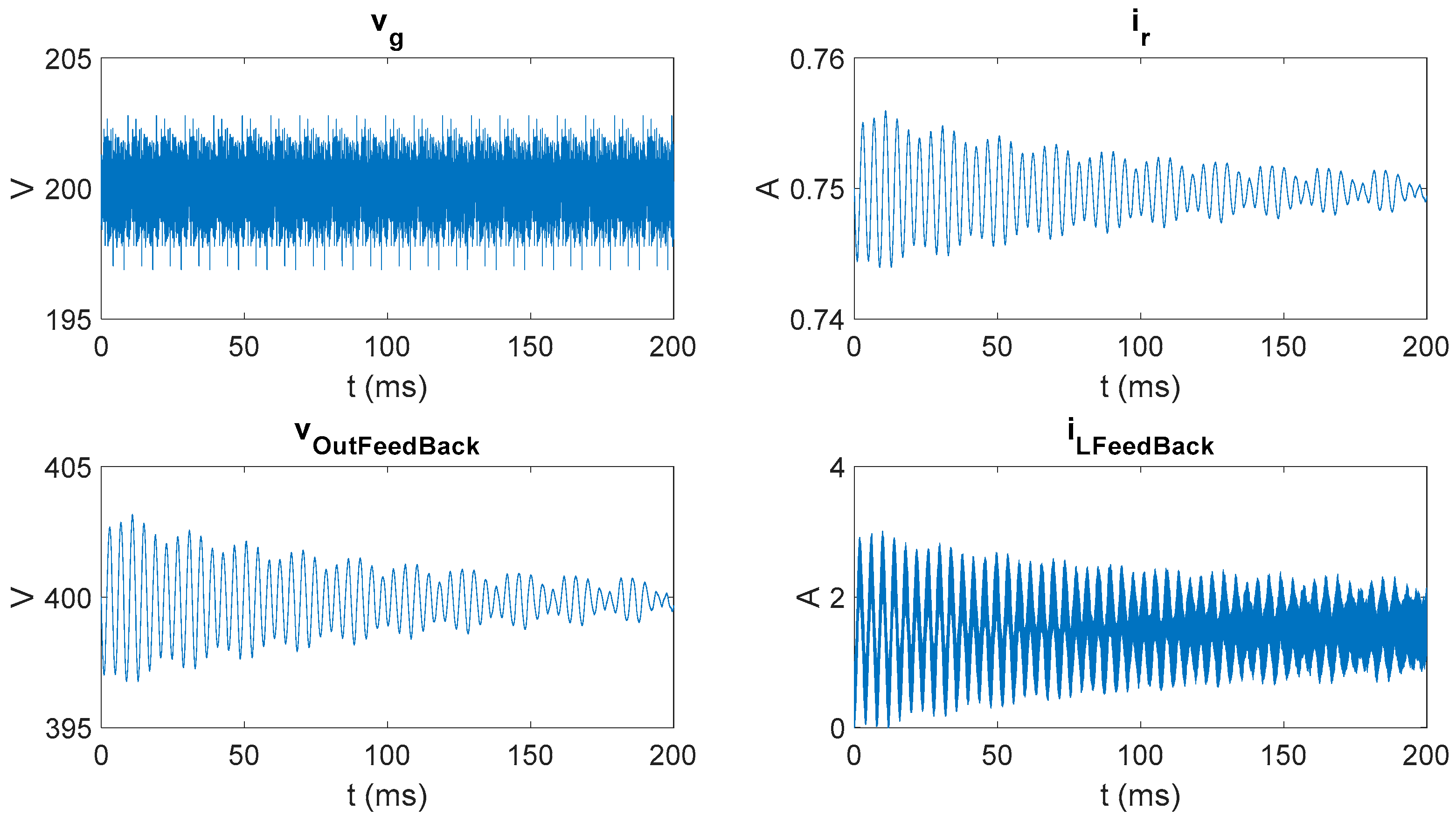
iL = 0 A. The waveforms of the inputs and feedback signals are shown in
Figure 3. Here,
iR has the same kind of waveform as
vout because a resistive load is simulated. Regarding
vg, which is an independent input, as this application example is a DC–DC conversion, it could be a constant. However, if it was constant, it would be difficult to study the necessary number of bits in its associated feedback signal (
voutFeedback), as will be explained later. That is why white noise is superimposed to the average value of 200 V, as shown in
Figure 3.
Analyzing
Figure 3, the number of bits that change in each signal can be extracted. For instance,
vout changes between approximately 397 and 403 V. Its maximum variation is 6 V, so a total of log
2 (6) bits, rounded up to 3, are changed. Then, the number of integer bits that really change in
vout is 3, which will be noted as Xmov (
vout) = 3. However, the total number of changing bits in
vout is Xmov + Y = 3 + Y, since all the fractional bits will also change. Using the same reasoning, for
vg (represented with Q9.3 bits) with a variation of 5 V, Xmov (
vg) = 3, but its total moving bits are Xmov + Y = 3 + 3 = 6 in
vg. For
iR, that is Q2.10 bits, a variation of 0.01125 A is obtained, so Xmov + Y = (−6) + 10 = 4 bits are changing, and finally for the
iLFeedback that varies 3 A, the changing bits are Xmov + Y = 2 + Y.
As previously explained, the first experiment checks the error when all the signals have 24 bits more than those theoretically necessary (as shown in
Figure 2), except
vg and
voutFeedback. Here,
vg is set to Q9.3, while
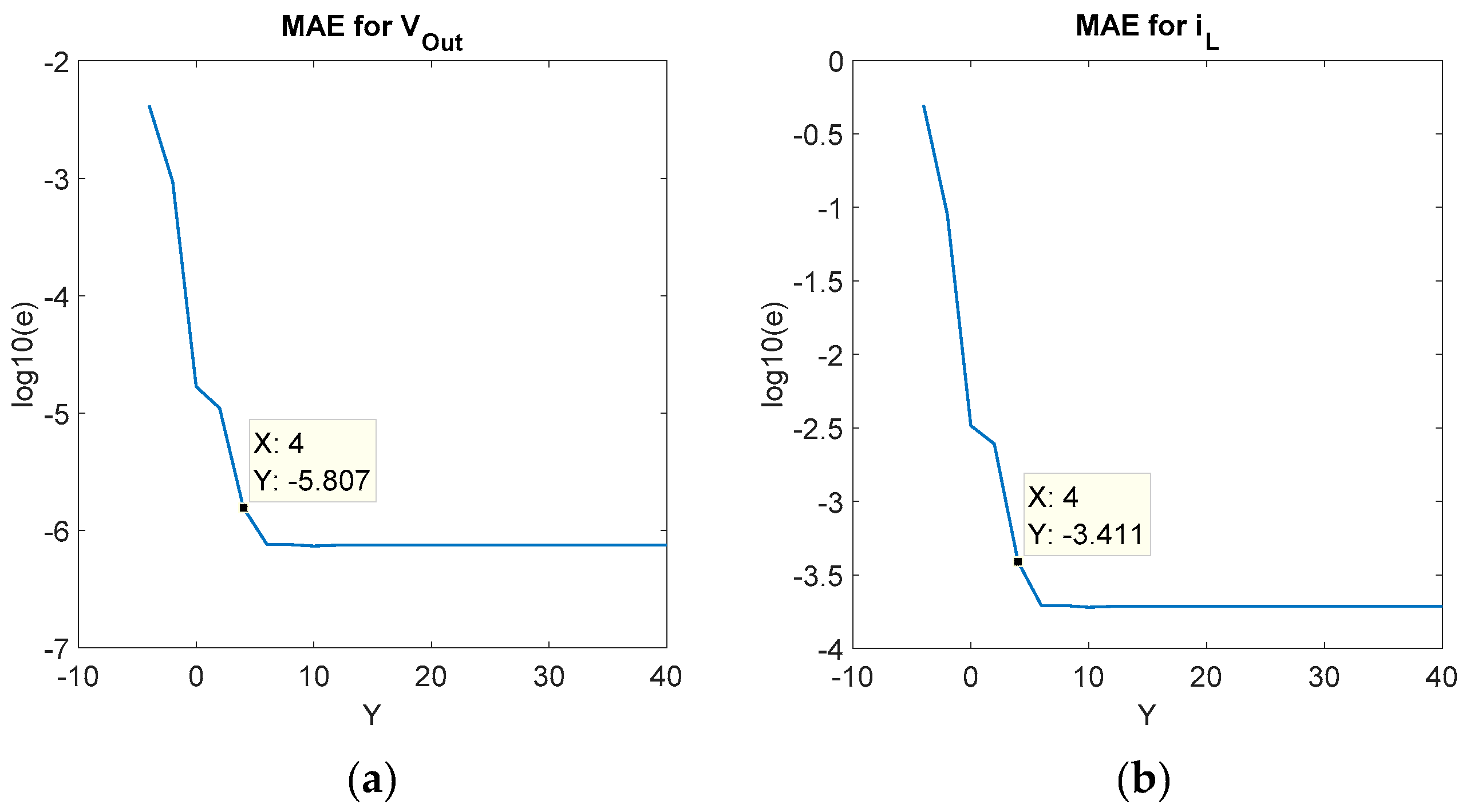
voutFeedback is Q11.Y with variable Y. Therefore, these two signals should be the main ones responsible for the error. The relative MAE in each state variable for this case is represented in
Figure 4a for
vout and
Figure 4b for
iL. The vertical axis is the relative MAE in logarithmic scale (so 0 means 100% error) and the horizontal axis is Y, the number of fractional bits of
voutFeedback. Y is moved from a maximum of 48 bits (24 of the original
vout in
Figure 2 plus the 24 extra bits) down to −3, when the relative error of the inductor current approaches 100%. The relative error of the output voltage is smaller, but in accordance with the smaller relative change of this state variable, as seen in
Figure 3. Regardless, the behavior in both state variables follows the same pattern. This agrees with the fact that the model is a loop in which the error in any point propagates to the rest of the model. The second conclusion is that the error stops decreasing after a certain number of Y bits is used (flat area of each series in the graphs). This reflects the fact that the signal with the highest error is responsible for almost all the error, and a slightly decrease of the error in other signals leads does not produce positive results. However, the left part of each series in the graphs shows that the error decreases as the number of Y bits increases almost linearly. Therefore, the error in that part of each series is mainly caused by the signal, which changes its number of bits,
voutFeedback, while the error in the flat part is mainly caused by another signal. As all other signals except
vg and
voutFeedback have 24 bits more than theoretically necessary, the signal causing the error in this right part is
vg.
Figure 4 also shows the frontier between both error-dominant parts, which is when Y (
voutFeedback) = 3. This is also the number of fractional bits of its associated input,
vg.
The same analysis of the error in the state variables,
vout and
iL, is done in
Figure 5. In this case, the other feedback signal,
iLFeedback, changes its number of fractional bits (Q8.Y) and
iR is set to Q2.10, so only these two signals can be the cause of the error, since the rest of the signals have 24 bits more than they need. In this case, Y is moved from 41 (17 + 24) down to −4. The same general conclusions can be extracted, while the frontier between error-dominant parts is around Y (
iLFeedback) = 0. However, the number of fractional bits in
iR is 10. This discards the possibility that the necessary number of fractional bits in each feedback signal must be equal to the number of fractional bits in its associated input. However, when analyzing the number of changing bits in both signals it can be seen that they are very similar in the error frontier: Xmov (
iLFeedback) + Y (
iLFeedback) = 2 + 0 = 2 bits, while Xmov (
iR) + Y (
iR) = −6 + 10 = 4 bits.
Therefore, the proposed hypothesis is that the total number of moving bits in each pair of feedback values and the associated input must be the same. This also agrees with the results of
Figure 4. In this case, Xmov (
voutFeedback) + Y (
voutFeedback) = 3 + 3 = 6 bits in the error frontier, while Xmov (
vg) + Y (
vg) = 3 + 3 = 6 bits. However, in order to confirm this hypothesis, additional results are desirable. These are extracted from a similar experiment with other simulation results.
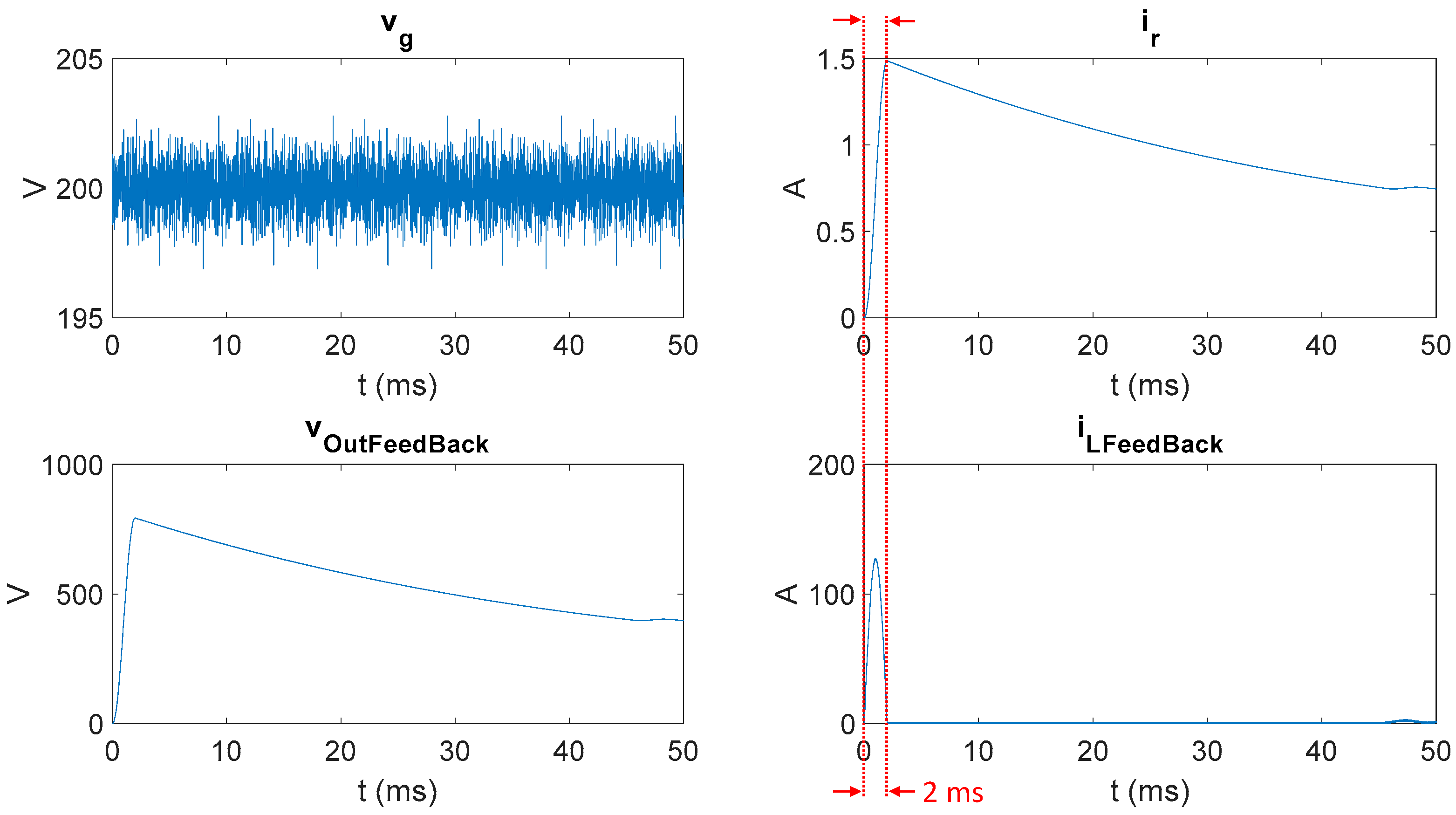
In this second set of simulations, a constant duty cycle with initial conditions
vout = 0 V and
iL = 0 A is used. The waveforms of the four signals under study are represented in
Figure 6 with these initial conditions, in contrast to
Figure 3, which shows the waveforms under other set of initial conditions. However, very different limits are reached in these new simulations, which significantly change Xmov. The new obtained values are Xmov (
vg) = 3, Xmov (
voutFeedback) = 10, Xmov (
iR) = 2, and Xmov (
iLFeedback) = 7.
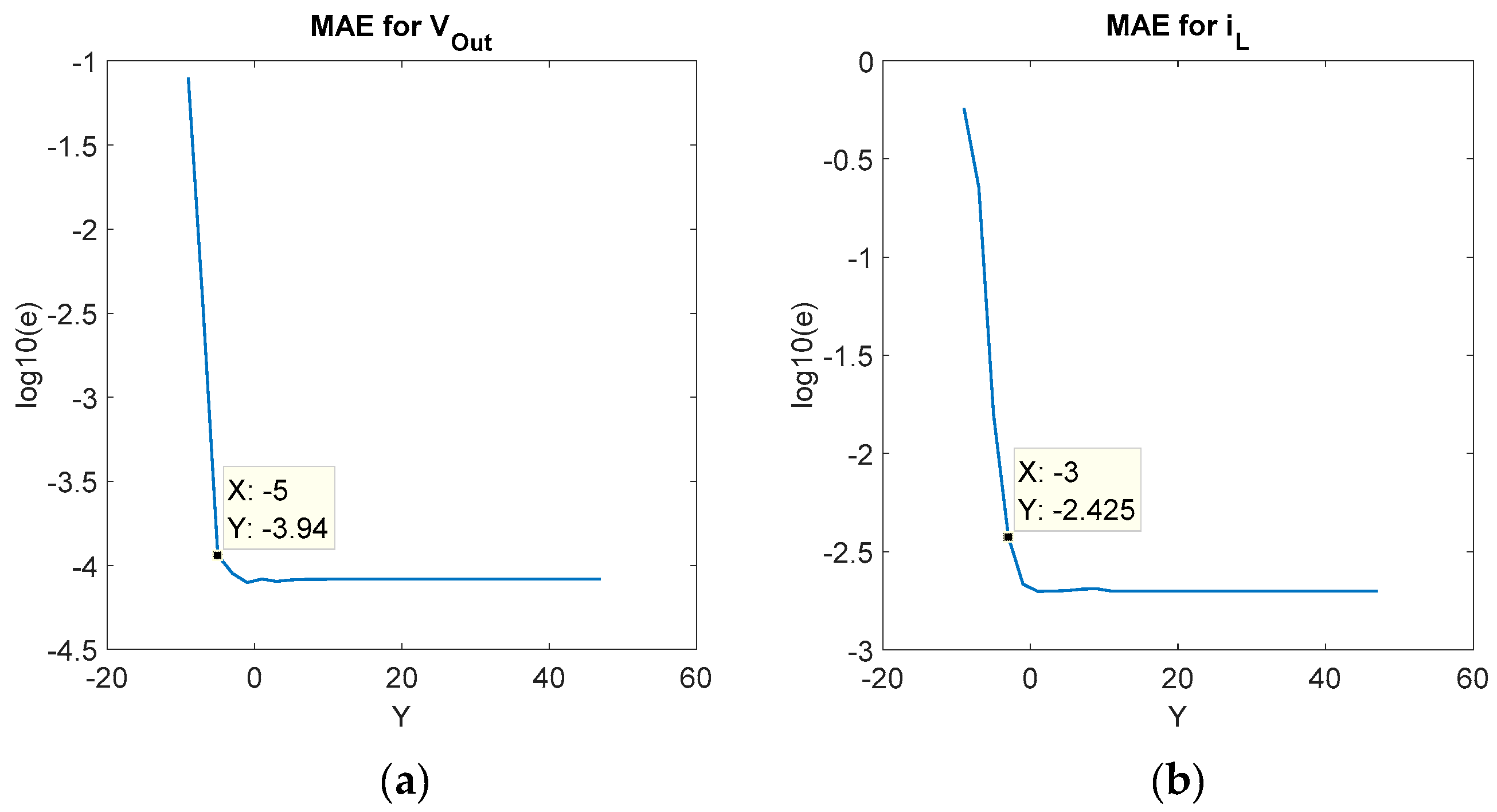
Again, the first error analysis is carried out by removing
voutFeedback, while
vg is set to Q9.3. The rest of the signals have 24 additional bits to discard if they are the source of error.
Figure 7 shows the relative MAE in both state variables. In this case, the error frontier is Y (
voutFeedback) = −5 or −3, depending on the state variable. Analyzing the total number of changing bits in the error frontier, Xmov (
voutFeedback) + Y (
voutFeedback) = 10 + (−5) = 5 or 10 + (−3) = 7 bits, while Xmov (
vg) + Y (
vg) = 3 + 3 = 6 bits, so the results are in agreement with the hypothesis.
Regarding the other pair of feedback input signals,
iLFeedback and
iR, an additional consideration must be taken into account. The number of moving bits of
iLFeedback is very different in two parts of the simulation. In the start-up, which lasts for 2 ms (marked in red color in
Figure 6), Xmov (
iLFeedback) = 7, since the current reaches 127.3 A starting from 0 A. However, after that short abrupt transient phase, the current dramatically decreases and in fact enters the DCM for a long time. Not only is the number of changing bits dramatically decreased, but the possible error is reset to 0 every switching period, since the current is forced to be 0 A. Therefore, the error comparison should be made only during that part of the simulation (first 2 ms) to avoid biased results because of the DCM mode resetting the error of
iLFeedback every switching period.
The error during those starting 2 ms is analyzed in
Figure 8. The error frontier is in Y (
iLFeedback) = 4, so Xmov (
iLFeedback) + Y (
iLFeedback) = 7 + 4 = 11 bits, while Xmov (
iR) + Y (
iR) = 2 + 10 = 12 bits, which is in good agreement with the hypothesis.
5. Discussion and Proposed Design Criteria
The conclusion of the previous results is that the number of moving bits (Xmov + Y) in a feedback signal must be equal or greater than those in its associated input (see Equation (12)) in order to reach the same level of error. Further additional fractional bits, Y, in the feedback signal are wasted since the error is then imposed by the input, for which the number of bits is externally set by some hardware restriction (e.g., number of bits in an ADC). However, this criterion of (Xmov + Y) would be difficult to use because, as has been previously seen, Xmov changes in the same model in different simulation scenarios. The question is how to set a reasonable number of bits for the feedback signals that will be enough for most simulation conditions, without unnecessary waste of resources and without having to know in detail all possible simulations conditions. Since X (feedback) is directly inherited from the state variable, the only parameter to determine is Y (feedback).
The proposed solution to set Y (feedback) is by simultaneously meeting the following three criteria:
In all the cases in which Xmov (feedback) ≥ Xmov (input), only with criterion I is Equation (12) met. For the cases in which Xmov (feedback) < Xmov (input), meeting criterion I is not enough to also fulfill Equation (12). However, Equation (12) will be met using criterion II as long as [Xmov (input) − Xmov (feedback)] ≤ [X (input) − X (feedback)].
With criteria I and II, the only possibility for not meeting Equation (12) is that Xmov (feedback) < Xmov (input) and [Xmov (input) − Xmov (feedback)] > [X (input) − X (feedback)]. This limits the possibility to cases in which Xmov (feedback) is quite low (i.e., the feedback signal (and therefore the state variable) has small changes during the simulation. When the changes are small, the error will also be smaller, so this possibility will be self-limited in its impact. For those cases, criterion III sets a natural ceiling for the possible error in that specific signal. This criterion is true for any signal and is a natural part of any fixed-point design. This last criterion assures an acceptable level of error, even when not meeting Equation (12). The error will be caused by the feedback and not the input, but the error will be low anyhow.
