Article

Realization of High-Performance Broadband Quadrature Directional Couplers in UMS PH25 Technology

by
Slawomir Gruszczynski
*,
Robert Smolarz
and
Krzysztof Wincza
Department of Electronics, AGH University of Science and Technology, 30-059 Krakow, Poland
*
Author to whom correspondence should be addressed.
Electronics 2019, 8(12), 1520; https://doi.org/10.3390/electronics8121520
Submission received: 5 November 2019 / Revised: 28 November 2019 / Accepted: 7 December 2019 / Published: 11 December 2019
(This article belongs to the Special Issue RF/Mm-Wave Circuits Design and Applications)

Abstract

:
The problem of the realization of broadband quadrature directional couplers in UMS (United Monolithic Semiconductors) PH25 is thoroughly investigated. The limitations of the selected technology are discussed with respect to directional couplers’ design. It is shown that, in such technologies, two major problems have to be overcome to achieve the high-performance of the resulting integrated couplers, i.e., the realization of appropriate coupling together with appropriate characteristic impedances, and the equalization of inductive and capacitive coupling coefficients that are inherently different in inhomogeneous dielectric structures. Three different solutions that allow for achieving strong coupling in the selected UMS PH25 process were selected and experimentally investigated, showing the possibility of such circuits’ realization. In each of the presented integrated couplers, capacitive compensation techniques were applied for coupling coefficients’ equalization.

1. Introduction

Quadrature directional couplers are well-known components that are often used in complex microwave circuits and networks [1,2,3,4]. Initially, such components were realized in a thick-film technology and interconnected with active devices placed on common supporting dielectric substrate [5]. Presently, it is a common practice to implement directional couplers in high frequency integrated circuits [6,7,8,9,10,11]. One frequently used solutions is to integrate branch-line directional couplers [1,7] and couplers designed with a quasi-lumped element approach due to simplicity of their design and physical realization [2,3,4,6,9,12,13]. However, such couplers feature inherently narrow operational bands, resonant reflections, and isolation responses, as well as a large imbalance between transmission and coupling characteristics, all of which limit their applications in broadband circuits and networks. A competitive solution is to implement coupled-line directional couplers in which operational bandwidths up to one frequency octave are easily achievable [14,15,16]. However, the price to be paid for a good frequency response is the difficulty of the coupled-line section’s design, and the constraints of the chosen fabrication technology impose additional challenges.
The conditions of an ideal coupled-line section’s realization have been investigated; in general cases of geometrically asymmetrical coupled-line sections, it is required that the inductive coupling coefficient kL and capacitive coupling coefficients kC are equal [17,18]:
k C = C 12 C 11 C 22 = k L = L 12 L 11 L 22
where Ci,j, Li,j are elements of per unit length capacitance and inductance matrices of a two-conductor coupled-line system. Additionally, the following impedance condition has to be fulfilled:
Z T i = L i i C i i
where ZTi, i = 1, 2 are the characteristic impedances of terminating lines. In case of symmetrical coupled-line sections, Condition (1) is equivalent to the equalization of even and odd mode phase velocities.
Over the years, several methods have been proposed that allow for the fulfillment of these conditions. Among the developed methods, two major groups can be distinguished. First are the methods in which the geometry of coupled-lines and dielectric stratification are appropriately selected, such that, for the desired coupling level, the coupling coefficients are equalized and the terminating impedances are equal to the required values [19,20]. Though the application of these compensation methods results in a very good performance of the designed coupled-line sections in terms of isolation and return losses, they require freedom in the dielectric stack-up selection and in the geometry of coupled conductors, which, in general, cannot be achieved in processes designated for monolithic integrated circuits. In such processes, it is common that the dielectric stratification cannot be modified and that the constraints on conductor dimensions and their relative placement are very tight. The second group of compensation methods utilizes lumped and distributed elements that are connected to coupled-line sections [18,21]. In such methods, it is assumed that additional lumped elements modify one of the coupling coefficients (usually the capacitive one) without affecting the other and the characteristic impedance of coupled lines; therefore, the equalization of coupling coefficients can be achieved along with the impedance condition.
In this paper, we present thorough investigations on the coupled-line directional couplers that are designed and fabricated in the chosen UMS PH25 technology. In this paper, three different techniques of 3-dB hybrid couplers’ realization are presented: (i) a three-strip coupled-line directional coupler, (ii) a Lange-type coupled-line directional coupler, and (iii) a directional coupler composed of coupled-line sections in conjunction with left-handed transmission-line sections. For each of the investigated directional couplers, a capacitive compensation technique is applied, resulting in the achievement of their good impedance match and directional properties. Moreover, we propose a modified compensation technique in which only one type of compensation elements is required—capacitors connected in-between the coupled conductors. We show how the compensation can be achieved in a broad frequency range and implemented in the chosen technology. Finally, experimental results of the three fabricated directional couplers are presented for comparison of the achieved properties and commented.

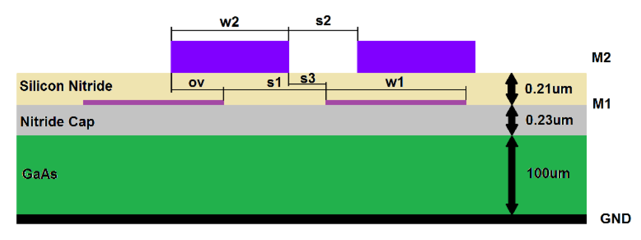
2. Analysis of Coupled-Line Section’s Realization in UMS PH25 Technology

The UMS PH25 technology is optimized for low noise and multipurpose operation up to 60 GHz. The process includes two metal interconnected layers, precision TaN resistors, high values TiWSi resistors, metal-insulator-metal (MIM) capacitors, air bridges, and holes through the substrate. The simplified stack-up offered in the technology is shown in Figure 1 and consists of three dielectric layers, namely a 100 um-thick GaAs layer with a dielectric constant εr = 12.8 and a loss tangent tg δ = 0.0065, a 0.23 um nitride cap layer with a dielectric constant εr = 7.2 (the loss tangent is not specified by the technology), and a 0.21 um-thin nitride layer (εr = 7.2, the loss tangent is also not specified), which separates the two metallization layers M1 and M2. The M2 is a gold, 3 um-thick low-resistivity metallization for the purpose of signal routing. The M1 is a thin layer of higher resistivity (0.06 Ohm/sq) mainly for the purpose of the fabrication of capacitor bottom electrodes.
With the presented stack-up, a number of coupled-line geometries can be proposed. However, the analysis of each of the considered coupled-line geometries needs to be conducted while taking the limitations of the technology into account. The major limitations that affect the design of coupled-line sections are listed in brief in Table 1. Below, we present the analysis of four cases of coupled-line geometries that are often utilized for the design of directional couplers. The numerical calculations of all coupled-line geometries were made with the use of Linpar software [22], which was also used in further development of the fabricated models.

2.1. Edge-Coupled Lines

The edge-coupled-line geometry is mainly limited by the minimum slot s2 between the coupled strips, a minimum that affects the maximum available coupling; for the minimum slot s2 = 8 um, the coupling k = 0.545 (C = −5.28 dB) can be obtained for a coupled-line section with a characteristic impedance equal to 50 Ω. The calculated coupling coefficient vs. slot s2 is presented in Figure 2a, whereas the calculated even and odd-mode dielectric constants are presented in Figure 2b. As is seen, the coupled-line geometry can be utilized primarily for weakly-coupled directional couplers, and the modal relative dielectric constants have different values. Therefore, the directional coupler’s design with this geometry would require some compensation techniques in order to obtain good directional properties for the coupler.

2.2. Two-Strip Asymmetric Coupled Lines

Another coupled-line configuration that can be considered in the UMSPH25 stack-up is a two-strip geometry, in which one of the strips is placed on the M1 layer and the other one is placed on the M2 layer. In such a structure, the two strips could either be separated and the the minimum slot s3 > 4 um has to be kept, or the two strips could overlap and the minimum overlapping ov > 2 um has to be ensured. Figure 3 presents the calculated capacitive and inductive coupling coefficients and strips’ widths for the case of separated strips vs. slot dimension, assuming the characteristic impedances of strips equal to 50 Ω. As can be seen, the achievable couplings k were not greater than 0.6, and it was not possible to realize higher couplings due to the required minimum slot width.
On the other hand, similar characteristics are presented for the case of overlapped strips in Figure 4. In this case, due to the very small thickness of the separating layer, and thus a high mutual capacitance between strips, the achievable coupling was very high. However, in this case there was a problem with the characteristic impedance, which was always much lower than 50 Ω and was also limited by minimum widths of the conductors. To conclude, the two-strip configuration can also be practically used for the realization of weakly coupled lines, similarly to the geometry described in Subsection A.

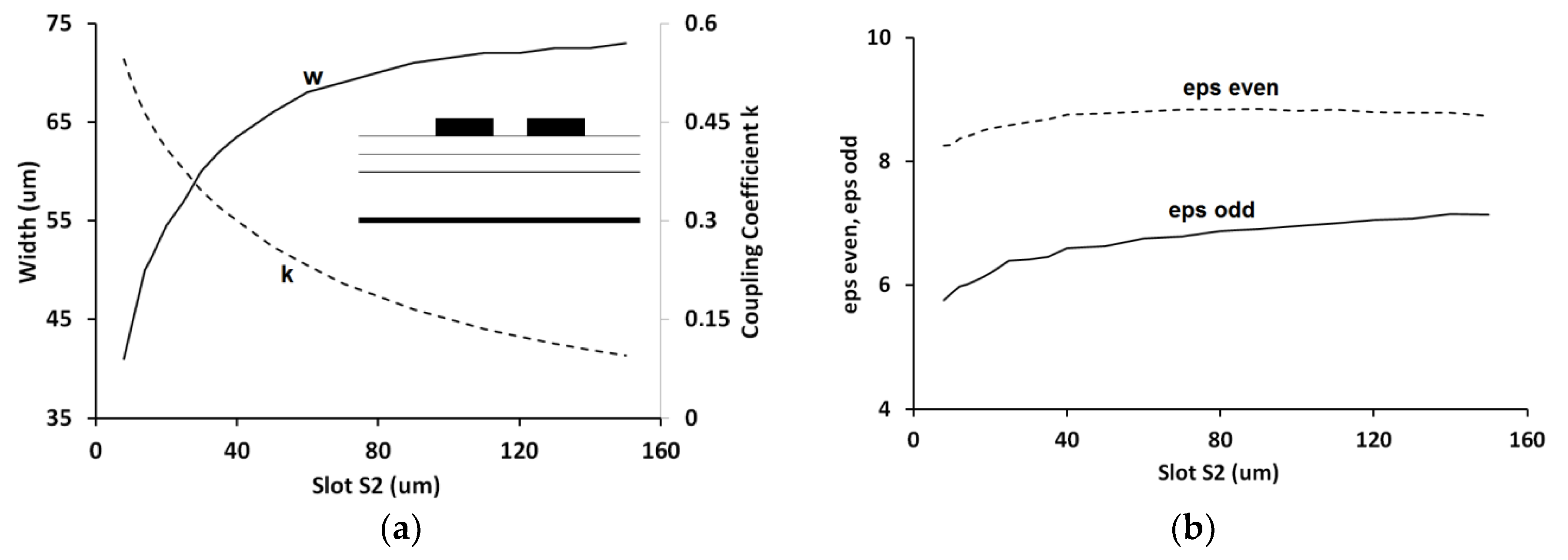
2.3. Three-Strip Asymmetric Coupled Lines

The three-strip coupled-line geometry, shown as an inset in Figure 5a, has been considered following its potential applicability for the design of 3-dB directional couplers, as was reported in [19]. In this configuration, the two conductors placed on the M1 layer are considered as one conductor (physically connected) and are coupled to the conductor on the top layer. The calculated coupling coefficients and the strips’ widths are presented in Figure 5. From the presented calculations, it can be seen that the mean coupling (algebraic mean between the two coupling coefficients) reached k = 0.71 (C = −2.97 dB) for the minimum slot s3 = 4 um. The inductive and capacitive coupling coefficients were not equal; hence, the directivity of such a coupled-line section is limited. However, as is described later in this paper, the capacitive compensation for such a section can be applied.

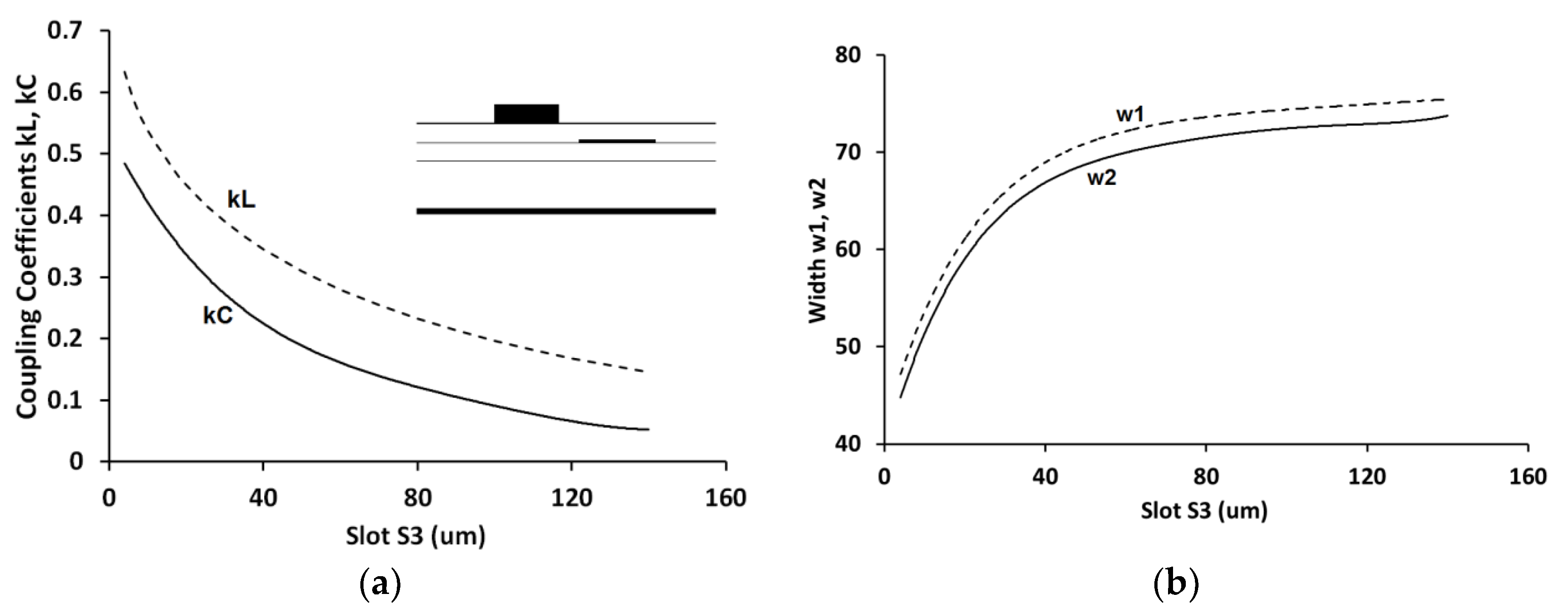
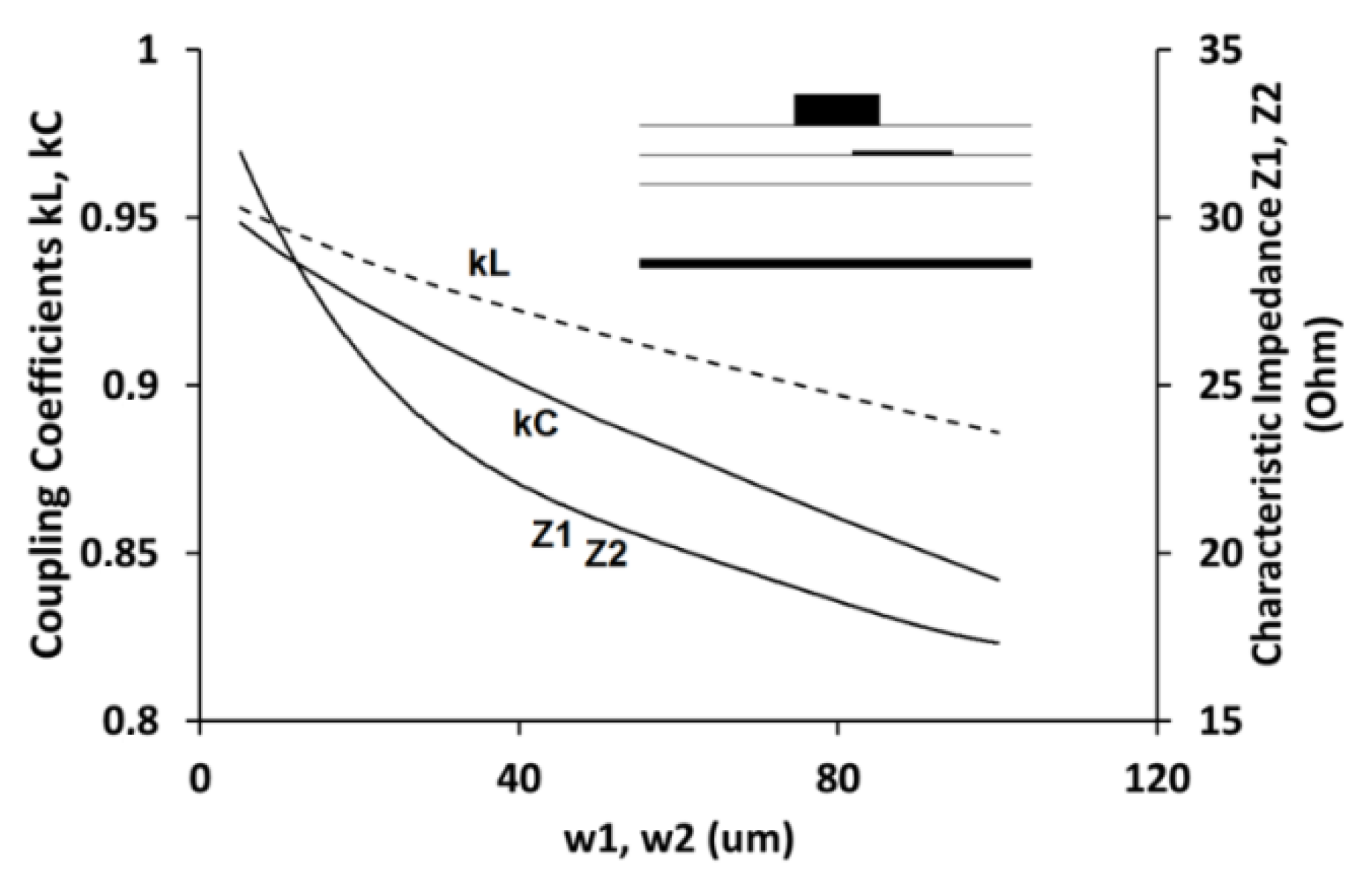
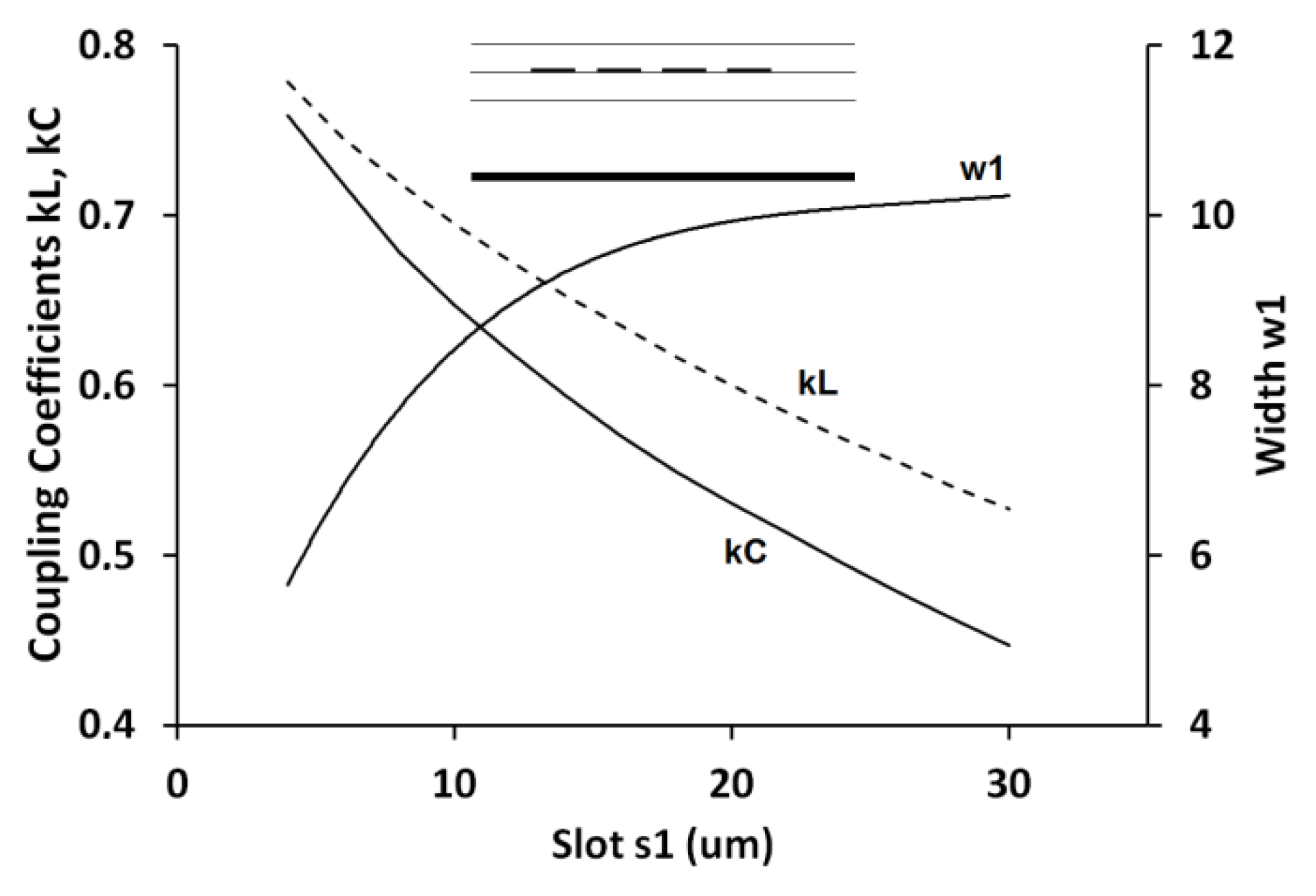
2.4. Interconnected Four Coupled Lines

Another considered geometry is the one shown as an inset in Figure 6 and consists of four coupled conductors. This is the configuration that is widely known and used for the design of Lange couplers, in which the conductors are appropriately interconnected (the first with the third and the second with the fourth) [14,15]. The calculated coupling coefficients and the strips’ widths are presented in Figure 6, and the structure allowed for a tight coupling realization k = 0.77 (C = −2.3 dB) with the constraints given in UMS PH25 technology. It is worth noting that the four-coupled-line geometry also features an inequality of coupling coefficients, similarly to the three-strip geometry. The requirement for the four-strip Lange coupler’s realization is the necessity of the bonding connection of non-adjacent strips, which can be made in UMS PH25 technology by using connections and M2 metallization.

3. Design of Coupled-Line 3-dB Directional Couplers in UMS PH25 Technology

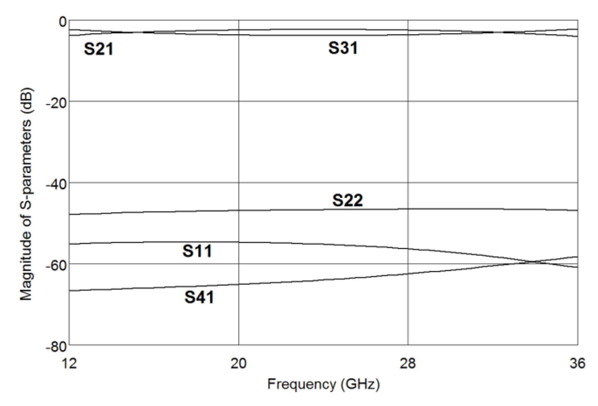
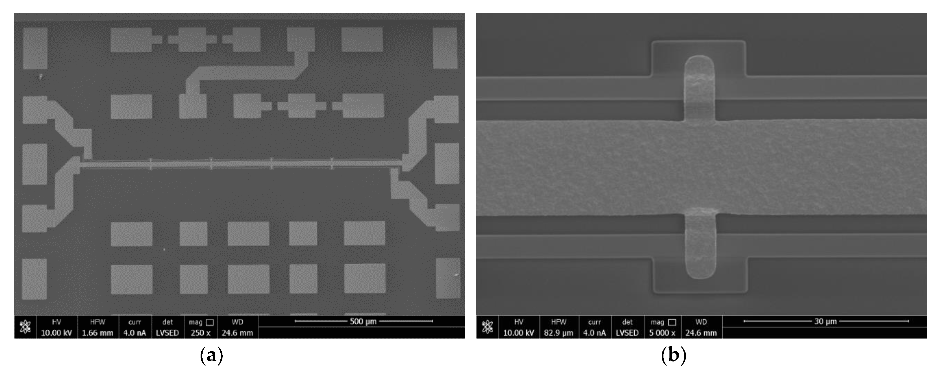
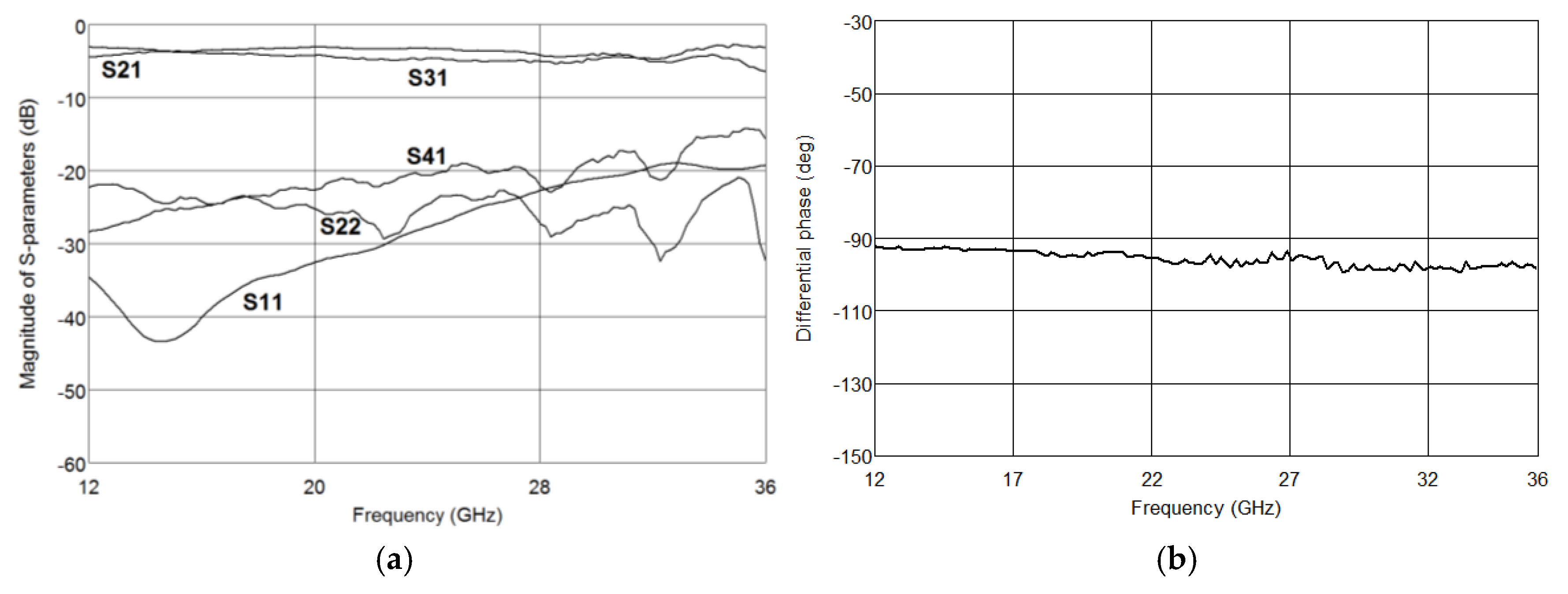
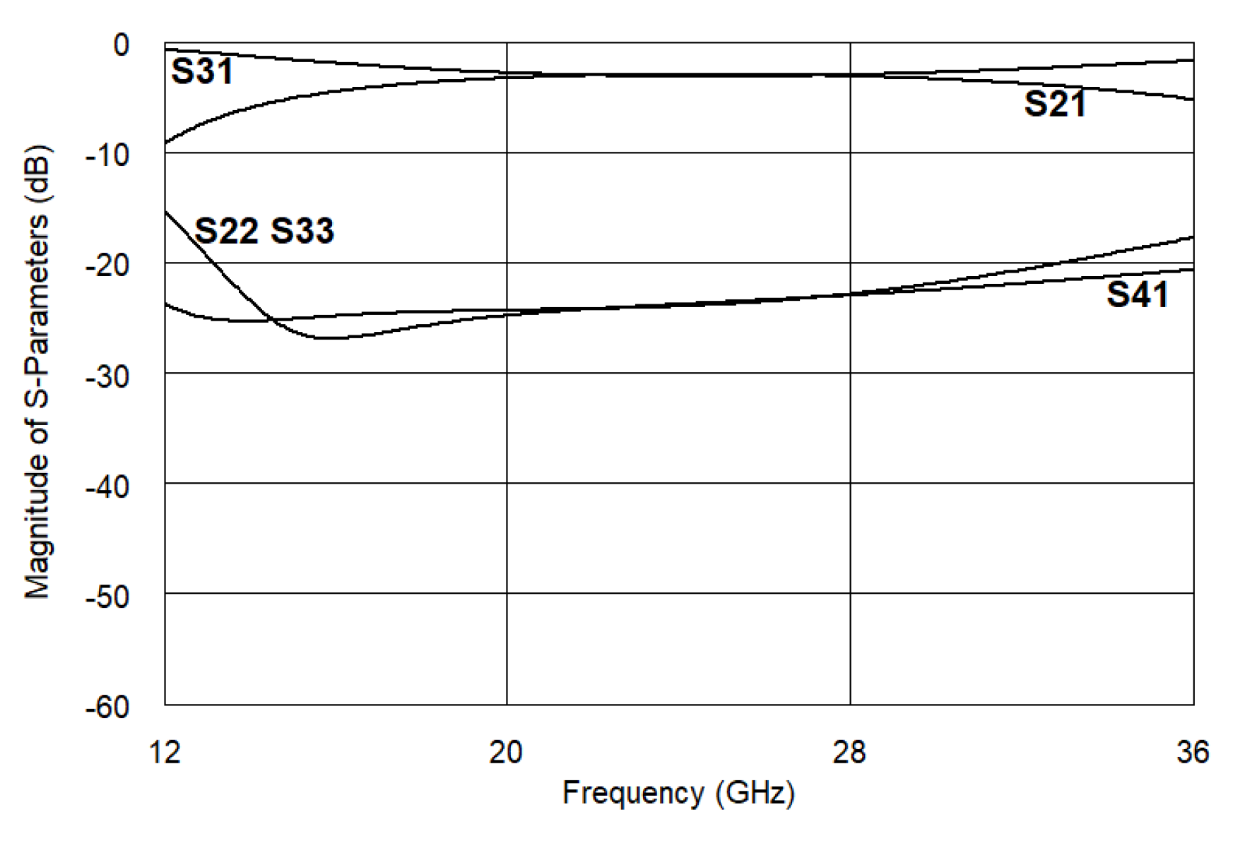
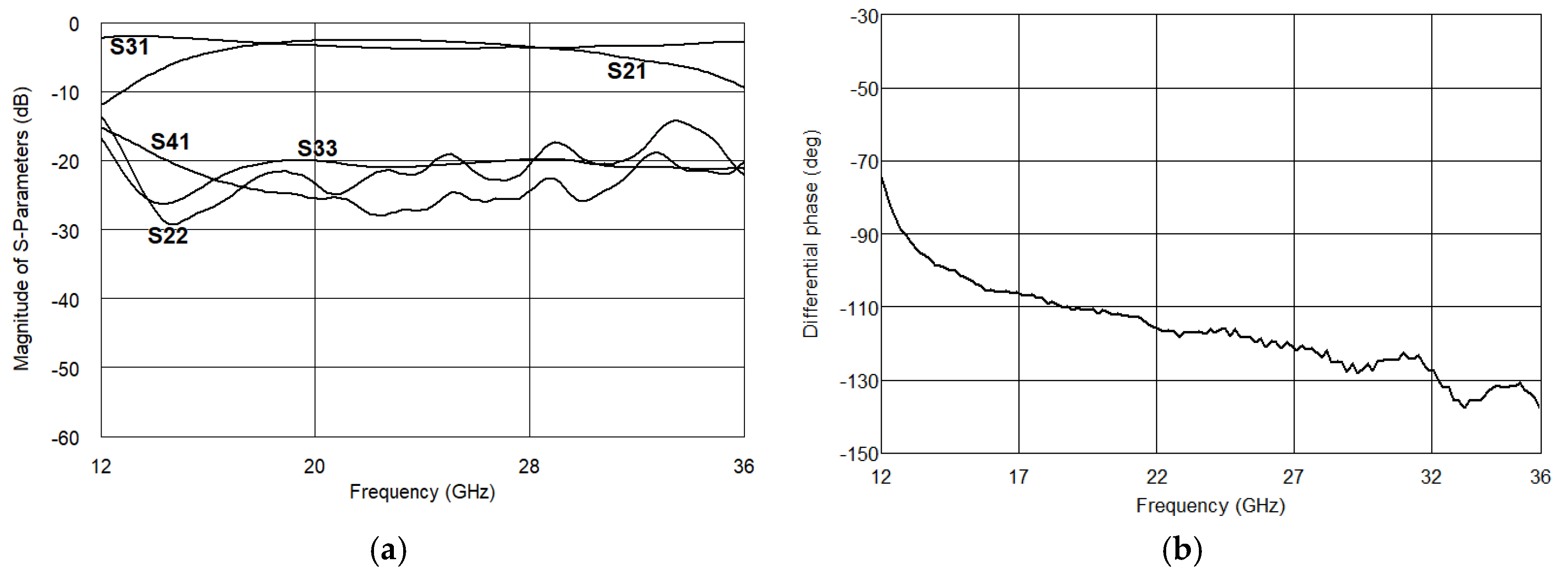
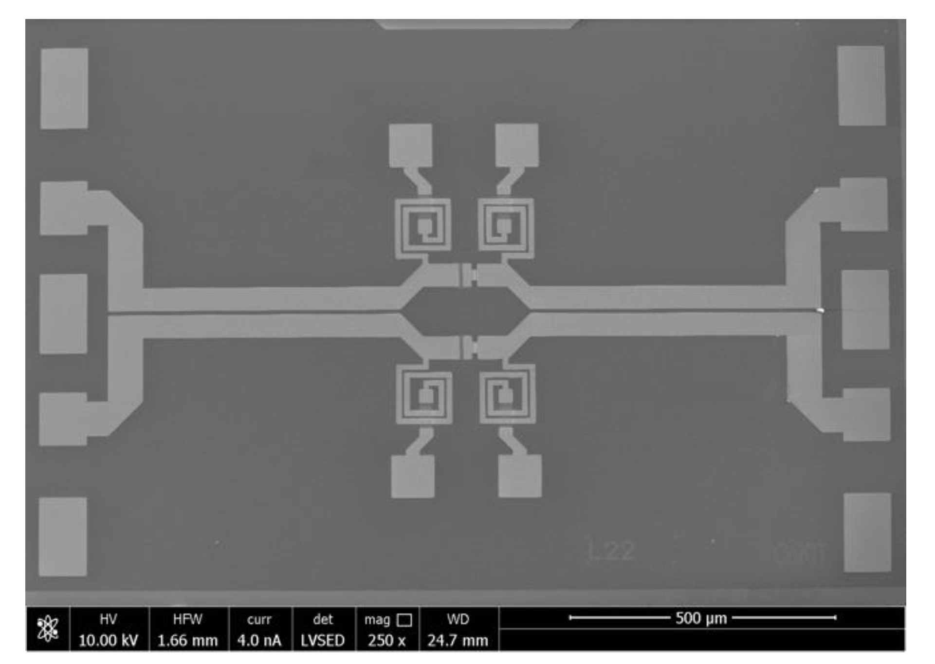
3.1. Three-Strip Asymmetric Coupled-Line Directional Coupler

Based on the analysis presented in the previous Section, the three-strip configuration is well suited for the realization of equal-split directional couplers. In this configuration, the coupling coefficients reached the level of k = 0.71; however, there was a large imbalance between the capacitive and inductive coupling coefficients that could have led to the deterioration of directive properties and reflections of the directional couplers. To further investigate the possibility of directional coupler’s design in this coupled-line geometry, an exemplary case of the geometry was theoretically and experimentally investigated. First, we investigated the deteriorative influence of the coupling coefficients’ imbalance on the properties of the coupled-line section. The coupled-line section’s geometry was designed in a way to maintain the 50 Ω terminating impedance and the mean coupling k = 0.707 (C = 3 dB), and the geometrical dimensions of such a section were as follows: w1 = 7.5 um, w2 = 34.5 um, and the slots between the strips s3 = 4 um. The obtained coupling coefficients were as follows: kL = 0.7632 and kC = 0.6497, and the reduced per-unit length matrices are:
L = [ 605.7 459.3 459.3 597.9 ] n H m ,   C = [ 243.8 156.6 156.6 238.3 ] p F m
The per-unit-length values were used to calculate the frequency response of the coupled-line section, and the results are presented in Figure 7. As can be seen, the section exhibited an equal power split at the center frequency, as predicted; however, the coupling coefficients’ imbalance resulted in a poor response in terms of isolation and return losses, which were on the level of 20 dB at the center frequency and gradually deteriorated with the frequency increase. It is worth underlining that the results were strictly theoretical and did not take the further deterioration of the response resulting from the necessary connection of the strips w1 , the connection of the input/output transmission lines, and the manufacturing accuracy into account. Hence, the expected overall performance of such a section would be, in practice, worse than the results presented in Figure 7.

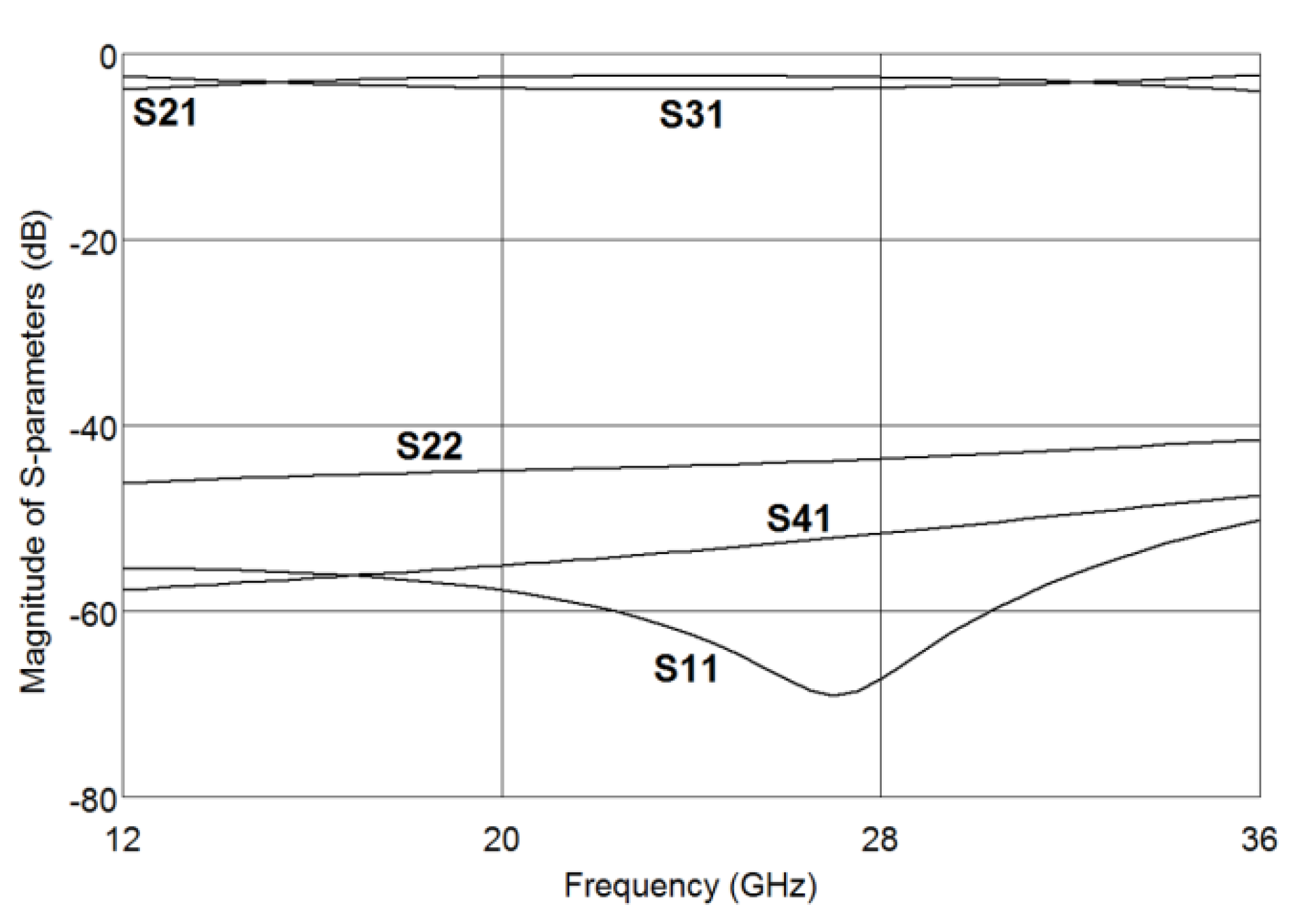
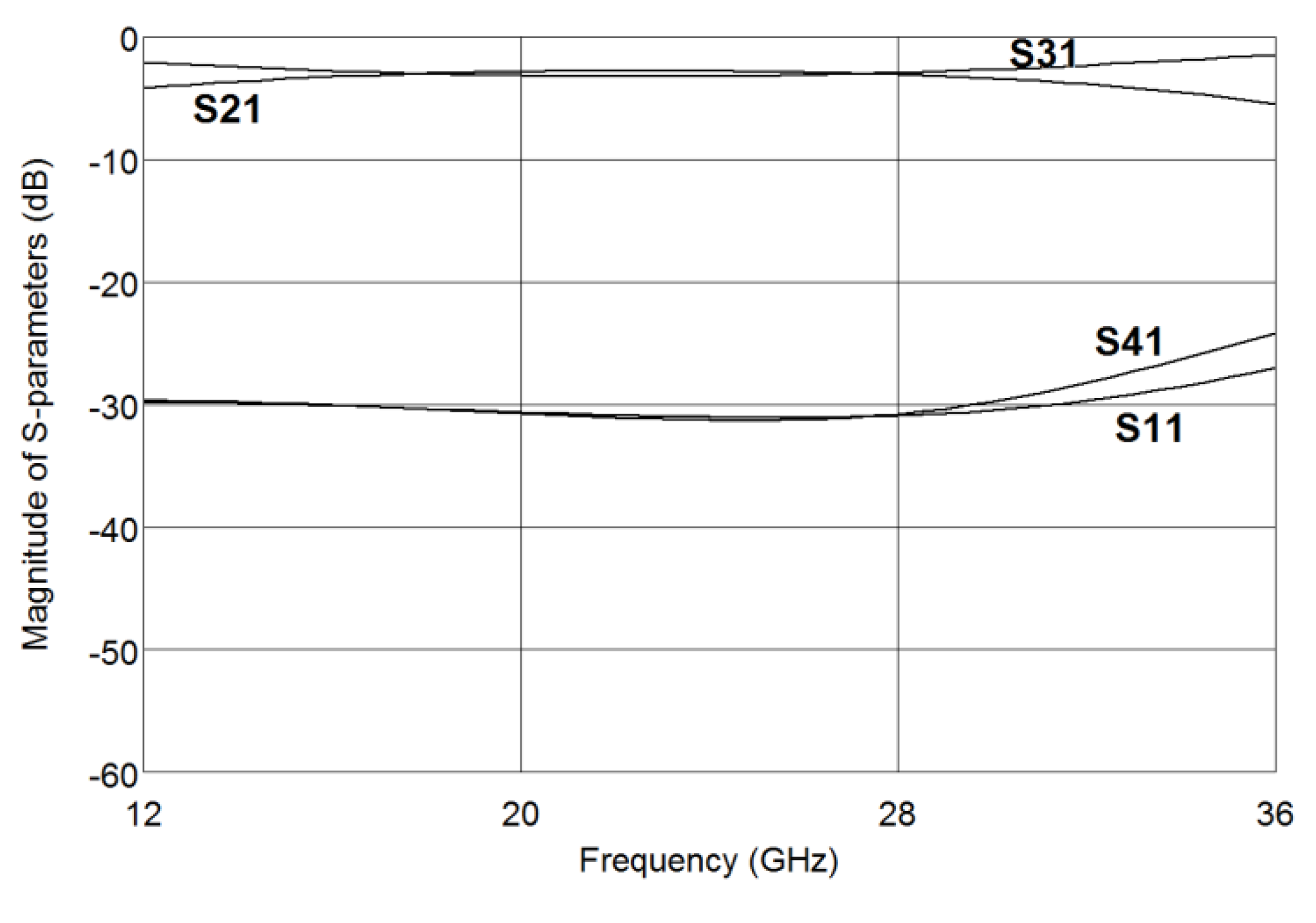
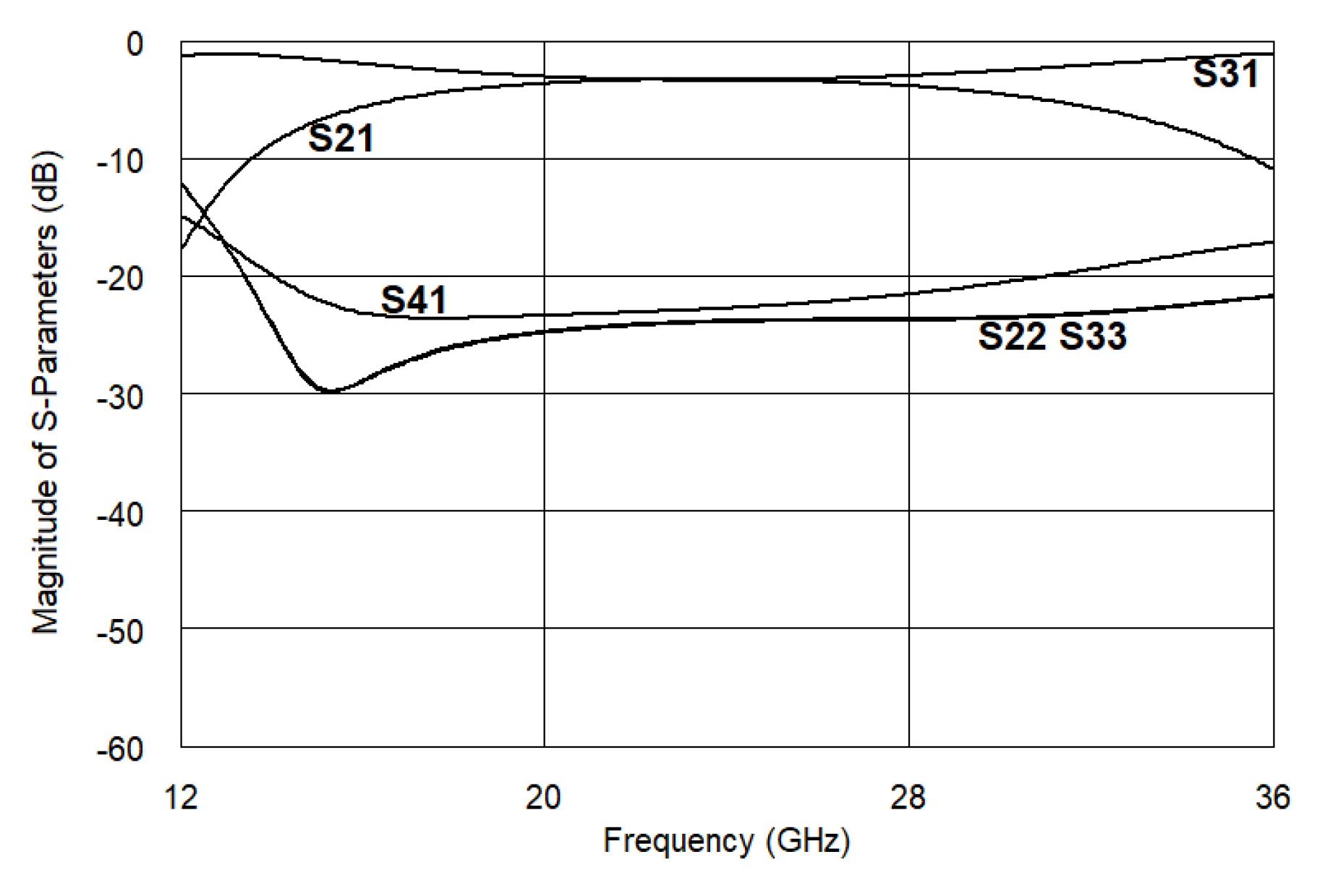
3.2. Compensated Three-Strip Asymmetric Coupled-Line Directional Coupler

The frequency response of the coupled-line section can be improved when an appropriate compensation method is applied, which results in the equalization of inductive and capacitive coupling coefficients. One possible approach is the utilization of the quasi-lumped-element compensation in which additional elements, such as capacitors and short compensating coupled-line sections, are connected to the compensated sections [18].
In this paper, we propose a novel method for coupled-line section’s compensation that is beneficial with respect to the previously published ones in terms of the number of required compensation elements. In the general approach presented in [18], to compensate coupled-line sections, it is assumed that three types of elements need to be utilized, i.e., compensating capacitors Ccm between coupled lines, compensating capacitors Cc1,2 connected between each of the coupled lines and a common ground, and short compensating sections of coupled lines. In the considered case, when the inductive coupling coefficient of the uncompensated section is greater than the capacitive one, i.e.,
kL > kC
it is possible to propose a compensation method in which only one type of elements connected between the coupled lines can be used, as is schematically shown in Figure 8. Such an approach is very well suited for application in monolithic technologies, where, typically, the interlayer capacitors are standard elements with a well-defined unit capacitance of large value, which results in small dimensions of such capacitors. In the proposed method, the initial geometry of the coupled lines was designed in such a way that, after adding compensating capacitors, the coupling coefficients are equal and are equal to the required value:
kL = kC = krequired
and the impedances of both strips are equal to the required terminating impedance (typically 50 Ω):
ZT1 = ZT2 = 50 Ω
The compensating capacitance can be calculated from the following equation:
k 2 r e q u i r e d = k 2 L = k 2 C = ( C 12 + C d ) 2 ( C 11 + C d ) ( C 22 + C d )
The compensating capacitance Cd can be calculated from the following quadratic equation:
Cd2(1 − kL2) + Cd [2C12 − kL2(C11 + C22)] + C122 − kL2C11C22 = 0
where Cd is the per-unit-length mutual compensating capacitance, and the positive solution is taken further into account. The solution of Equation (7) gives the value of the capacitance that needs to be added to the coupled-line geometry to equalize the coupling coefficients, but such a modification also contributes to the characteristic impedances of each line. Therefore, in order to maintain the required impedance, this influence must be considered by including the compensating capacitance in the impedance relations (Equation (2)), as follows:
Z T 1 = L 11 C 11 + C d ,   Z T 2 = L 22 C 22 + C d
The set of Equations (7) and (8) allows one to find a structure for which the coupling coefficients are equalized and the impedances are as desired under the condition that, for the calculated geometry, the compensating capacitance Cd is added between coupled lines. In practice, Cd is realized as a number of lumped capacitors Ccm connected along the lines, and the capacitors’ values can be calculated as:
C c m = C d n l
where l is the physical length of the coupled lines and n is the number of lumped capacitors that realize the required capacitance Cd.
Practically, to design a section, one needs to iteratively modify the geometry and calculate Equations (7) and (8) to meet the required impedances. The overall coupling will be equal to the inductive coupling coefficient that is not influenced by the compensation. The number of possible solutions is infinite, but, practically, the idea is to obtain the values of Ccm that are as small as possible to make the practical realization possible.
To illustrate the proposed compensation procedure, the initially considered section shown in Figure 7 was compensated. The section’s geometry was redesigned, and the following geometry was found: w1 = 4 um, w2 = 17 um, and the slots between the strips s3 = 4 um. The obtained coupling coefficients without the compensating capacitance are as follows: kL = 0.7658 and kC = 0.6452, the reduced per-unit length matrices were equal:
L = [ 725.9 773.7 553.7 720.1 ] n H m ,   C = [ 193.1 122.6 122.6 187.2 ] p F m
for which the terminating impedances were ZT1 = 61.31 Ω and ZT2 = 62.02 Ω. The compensating capacitance calculated for the structure was Cd = 97.92 pF/m, for which the capacitive and inductive coupling coefficients became equal, i.e., kC = kL = 0.7658, and the terminating impedances were equal ZT1 = 49.94 Ω and ZT2 = 50.26 Ω. The modified capacitance matrix with the included compensating capacitance equaled:
C = [ 291.0 220.6 220.6 285.1 ] p F m
The calculated scattering parameters of the compensated section are presented in Figure 9. As can be seen, the section was very well matched, and the isolation of such a section was nearly ideal. A similar response is presented in Figure 10, where the distributed capacitance Cd was replaced with the lumped capacitors. In this case, five capacitors were applied with the values calculated from Equation (9) as Ccm = 22 fF. The coupled-line directional coupler was designed with the UMS PH25 design rules and was electromagnetically analyzed with the use of AWR Microwave Office software. The results of electromagnetic simulations are presented in Figure 11. Both isolations and return losses were better than 26 dB at the center frequency, and the response was significantly improved with respect to the theoretical uncompensated section shown in Figure 7. The SEM photographs of the fabricated directional coupler are presented in Figure 12, where the additional compensating capacitors are shown in close view. The measured response of the fabricated directional coupler is presented in Figure 13. As seen in the figure, the coupling of the measured coupler was close to the designed value, the return losses were better than 24 dB at the center frequency, and the isolation was better than 20 dB. The differential phase error did not exceed 5.5 deg at the center frequency. The measurements were performed with the PNA N5224A VNA and the GSGSG probes from Cascade. The test set was calibrated using the short-open-load (SOL) technique. The calibration standards were made in the same technological run as the directional coupler and are visible in Figure 12a above and below the coupler.

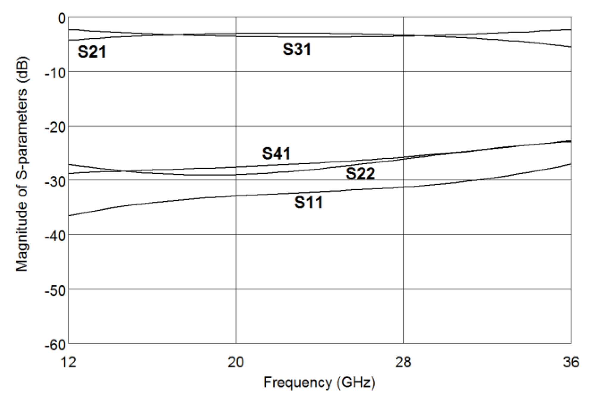
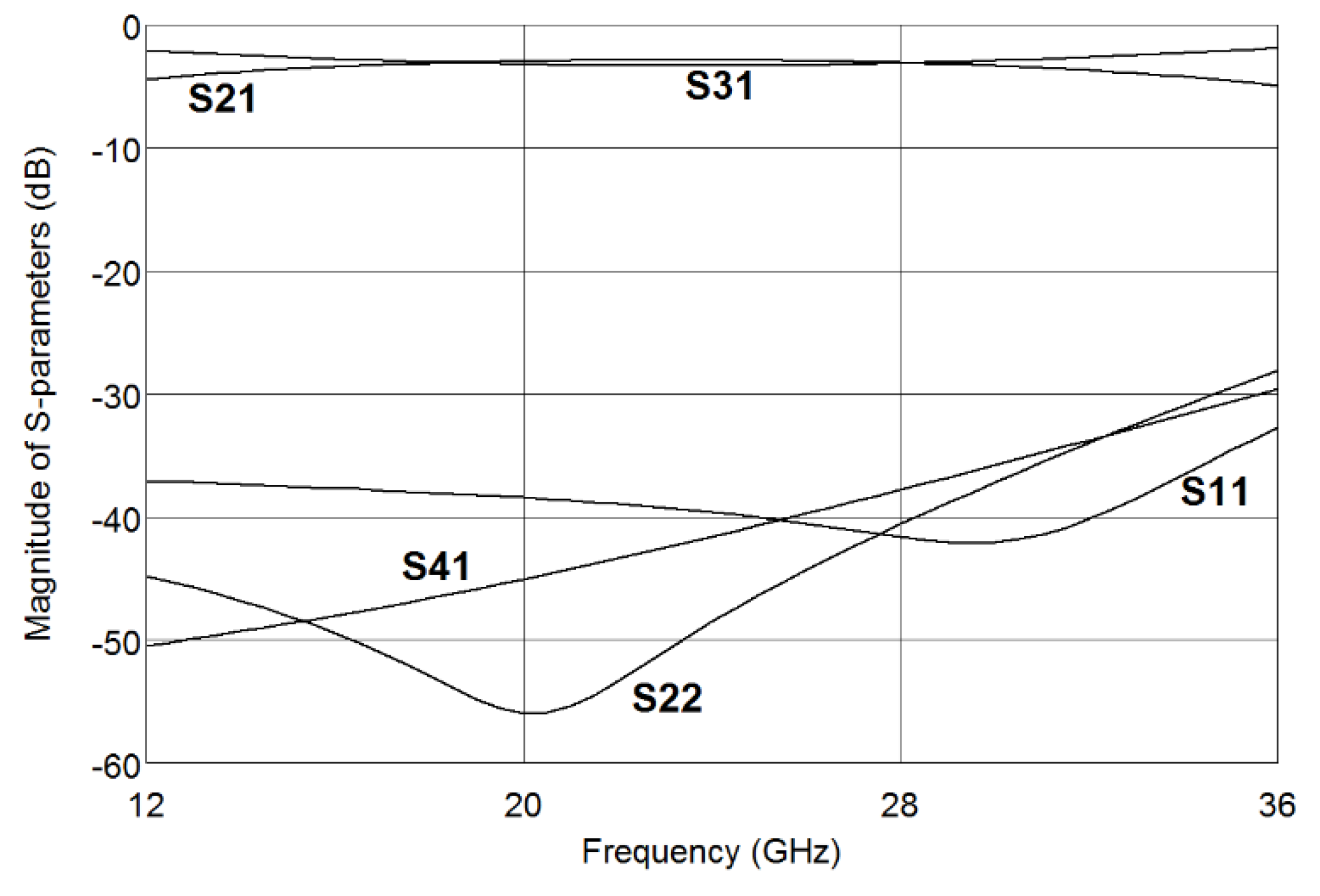
3.3. Lange-Type Compensated Directional Coupler

As was shown in Section 2, the interconnected four-strip coupled lines can be successfully used in UMS PH25 technology to obtain a strong coupling between lines. However, similarly to the previous case, the inductive and capacitive coupling coefficients were also unequal. Initially, the section was designed without compensating capacitances, and the following geometry was found: w1 = 6.7 um and s1 = 6 um. The coupling coefficients were kL = 0.7447 and kC = 0.7165, and the terminating impedances were ZT1,2 = 50.04 Ω. The frequency response of such an uncompensated section is presented in Figure 14.
Since the coupling coefficients’ imbalance was smaller than in the case of the three-strip section, the response in terms of isolation and return losses theoretically reached 30 dB. However, the response could be significantly improved, as shown in Figure 15, by using the method described in the previous section, and a small value of compensating capacitance Cd = 26.6 pF/m was needed to compensate the section. The small value of the compensating capacitance could be realized together with the realization of bounding connections between the strips that constituted the Lange coupler. The compensating capacitance Cd was realized as five lumped capacitors with a capacitance Ccm = 5.9 fF and were designed as 5 um-wide ribbons that bonded the conducting strips and were elevated 2 um above the surface of the chip (2 um air spacing of the ribbon above the top layer). The designed compensated Lange directional coupler was electromagnetically analyzed, and the results are presented in Figure 16.
Further, the coupler was fabricated in UMS PH25 technology, and the SEM photographs of the coupler are shown in Figure 17. The detailed view of the bounding ribbons shown in Figure 17b is worth noticing, as these ribbons served as necessary compensating capacitors between coupled lines. The designed Lange directional coupler was measured, and the results are presented in Figure 18. As can be seen, the results of measurements were close matches to the ones obtained from simulations. The measured isolation of the coupler was not worse than 28 dB at the center frequency, which proves that the coupled-line geometry was well-balanced in terms of coupling coefficients’ equality. The differential phase error did not exceed 5 degrees at the center frequency.

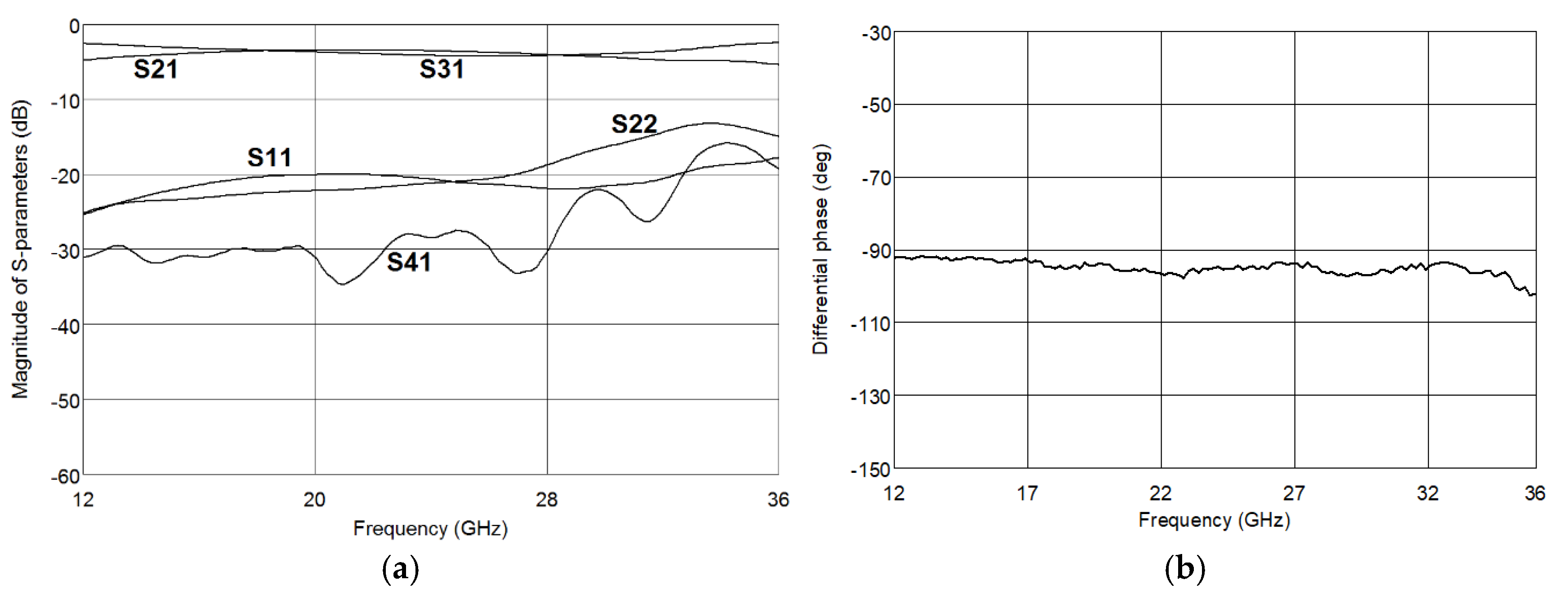
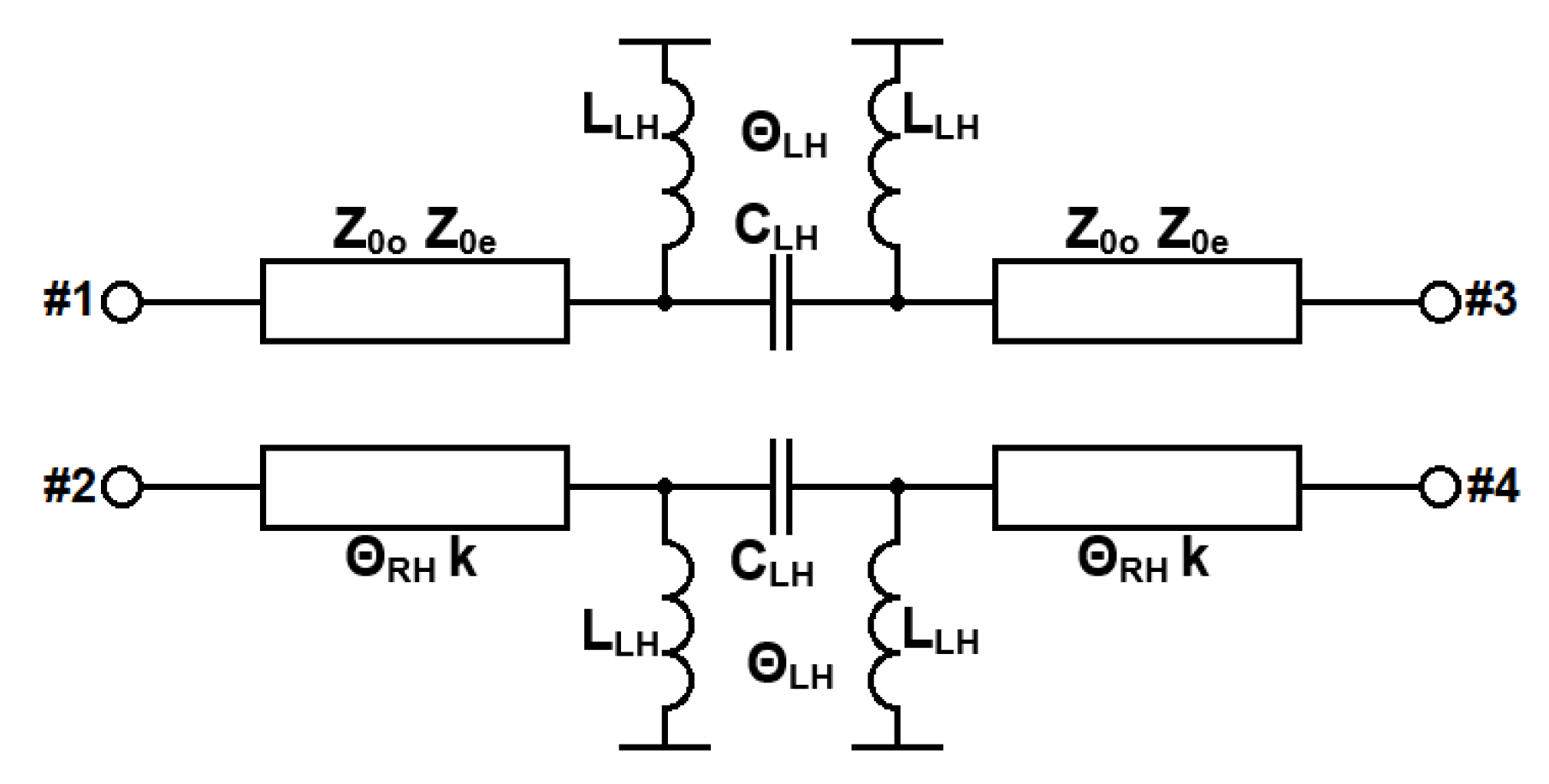
4. Design of 3-dB Directional Coupler with Left-Handed Transmission-Line Sections

Multi-conductor coupled lines are one of the most popular techniques for the realization of directional couplers. On the other hand, it has been shown in literature that couplers based on left-handed transmission lines can achieve relatively high coupling coefficients without the requirement of strong coupling in coupled-line sections [23,24]. In [23], the authors proposed a novel class of components in which relatively high coupling coefficient could be obtained in wide operational band. Such topology is presented in Figure 19 and was composed of two coupled-line sections between which the uncoupled left-handed sections were inserted. The left-handed sections were defined by their electrical length ΘLH and could be approximated with lumped elements, i.e., inductors LLH, and capacitors CLH, whereas the coupled-lines sections were defined by impedances Z0o, Z0e, electrical length ΘRH, and coupling k. It has been shown that the utilization of left-handed circuits can increase the coupling coefficient of the entire directional coupler, while the k of coupled sections can be relatively small [23,24].
In this paper, the directional coupler that followed the idea presented in Figure 19 was designed for comparison with the techniques presented in the previous section. First, the scattering parameters of the directional coupler that were composed of ideal elements, i.e., k = 0.566, Z0e = 88.01 Ω, Z0o = 28.40 Ω, ΘRH = 55.4°, LLH = 0.97 nH, CLH = 0.216 pF, were calculated, and the results are presented in Figure 20. The presented coupler was matched to the 50 Ω terminating impedances. It can be noticed that the chosen coupling coefficient k was smaller than the maximum coupling of the directional coupler and was chosen as the maximum that could be obtained for the symmetrical edge-coupled geometry in UMS PH25 technology.
Second, an investigation of the influence of inequality of the modal dielectric constants on the couplers’ response was conducted. For the considered technology and the geometry of two conductors on the M2 layer with the dimensions w2 = 48 um and s2 = 8 um, the following values of the modal dielectric constants were found: εe = 8.507 and εo = 6.645. The calculated frequency response that took into account different electrical lengths of the coupled-line sections for even and odd modes is presented in Figure 21. As can be seen from the obtained characteristics, the effects of modal permittivities’ inequality were not negligible and resulted in both decreased return losses and a decreased isolation of the considered directional coupler. In the calculations, the parameters of the left-handed section were tuned to the best performance and were chosen as LLH = 1.15 nH and CLH = 0.318 pF.
In order to improve the performance of the directional coupler, the compensation method presented in the previous section was once again utilized for each of the coupled-line sections shown in Figure 19. The coupled line geometry was recalculated, and the corrected dimensions of coupled conductors were found; these were: line width w2 = 43 µm and space between lines s2 = 8 µm. The additional compensating capacitance Cd was found, and it was equal to 37.74 pF/m. Figure 22 shows the calculation results obtained for the compensated 3-dB directional coupler with left-handed transmission-line sections. In comparison to the not compensated one, an isolation improvement could be easily seen. Moreover, return losses were also improved.
The presented directional coupler that consisted of left-handed transmission-line sections can be easily implemented into UMS PH25 technology due to the fact that all required components such as inductors and capacitors are available in the process. Based on the topology presented in Figure 19, the electromagnetic simulations of the 3-dB directional coupler operating at 24 GHz center frequency were performed in the AWR Microwave Office environment. The left-handed section was defined by inductance LLH = 0.57 nH and capacitance CLH = 0.27 pF. The compensation elements were realized by using two metallization layers—M2 and M1, which forms a simple MIM capacitor. In the considered coupler, four such capacitors were utilized with values equal to 12.6 fF. The results of the EM simulations are presented in Figure 23. As can be seen, the isolation was greater than 22 dB, and reflection coefficients were lower than −23.7 dB for the center frequency. To verify the applicability of the proposed compensation method in the considered topology, the 3-dB compensated directional coupler was fabricated and measured. The obtained measurements are shown in Figure 24 and are in good agreement with the simulation results. The return losses of the measured directional coupler were better than 20 dB, and the isolation was greater than 25 dB at the center frequency. The differential phase response featured large error with respect to 90 deg value and reached 27 deg at the center frequency. This was caused by the application of the left-handed section that distorted the phase response. In Figure 25, a SEM picture of the fabricated directional coupler is shown.

5. Conclusions

In this paper, a comprehensive study on the realization of 3-dB directional couplers in UMS PH25 GaAs technology has been presented. As shown, the geometry of the conductors and dielectric layers, together with the constraints on the geometrical dimensions, did not allow for a straightforward realization of 3-dB directional couplers. However, the techniques in which multiconductor coupled lines are utilized can be satisfactory utilized in the directional couplers’ design. The important issue in such couplers’ design is the utilization of the compensation technique that allows for the equalization of the coupling coefficients and, therefore, for the improvement of achievable isolation and return losses. In this paper, the capacitive compensation technique has been proposed, one which allows for the compensation of the coupled lines with only single-type compensating elements, namely the capacitors connected between the coupled conductors. Such components can be fabricated in UMS PH25 technology, in which an additional metallization layer with thin dielectric spacing is available for this purpose. Moreover, the possibility of the realization of directional couplers with left-handed sections of transmission lines has been investigated. The obtained experimental results are presented for comparison in Table 2 and were compared with similar designs published otherwise. As is seen, the three first directional couplers published in [10,11,12] featured a rather narrow frequency response in terms of power split, in the sense that the characteristics crossed each other in a single frequency point of intersection. Such a response featured large imbalance between the transmission and coupling characteristics. The remaining directional couplers, i.e., [14,15,16] and these shown in this paper, featured a wide response in terms of transmission and coupling with their double crossing character. Therefore, they also featured a small imbalance in wide operational bandwidth. Among the ‘wide-response’ couplers, the ones developed in this paper featured good properties in terms of return losses that were always better than 20 dB at the center frequency. Moreover, the achieved isolations were very good and oscillated between 28 dB for the Lange-type coupler and 20 dB for the three-strip directional coupler. The isolation of the coupler presented in [14] was better than the one obtained in this paper; however, in that realization, a thick dielectric separation between coupled conductors was applied, one which cannot be used in the investigated fabrication technology. The calculated total insertion losses, based on the measured results, at the center frequency of 24 GHz for the three fabricated couplers equaled 0.98, 0.71 and 0.68 dB for the three-strip directional coupler, Lange-type directional coupler, and the directional coupler with the left-handed transmission-line section, respectively. The size of the three-strip and Lange-type couplers were similar and equaled 83 × 1228 and 74 × 1205 um, respectively. The coupler with the left-handed section occupied a larger area of 710 × 1216 um due to the necessity of spiral inductors’ realization. The achieved good properties in terms of isolation and return losses, together with low total insertion losses, were obtained with the proposed compensation technique, which is a good candidate for the realization of coupled-line directional couplers in other competitive fabrication processes.

Author Contributions

Conceptualization, S.G. and K.W.; investigation, R.S.; methodology, K.W.; supervision, S.G.; writing—original draft, S.G., R.S. and K.W.

Funding

This work was partially supported by the National Research Centre Poland under contract no. UMO-2016/21/B/ST7/02200 and in part by the Polish Ministry of Science and Higher Education under subvention funds for the Department of Electronics of AGH.

Acknowledgments

The authors wish to thank UMS Foundry team for their substantive support during design process, and fabrication.

Conflicts of Interest

The authors declare no conflicts of interest.

References

  1. Ellinger, F.; Vogt, R.; Bachtold, W. Ultracompact reflective-type phase shifter MMIC at C-band with 360° phase-control range for smart antenna combining. IEEE J. Solid-State Circuits 2002, 37, 481–486. [Google Scholar] [CrossRef]
  2. Kosuge, A.; Mizuhara, W.; Shidei, T.; Takeya, T.; Miura, N.; Taguchi, M.; Ishikuro, H.; Kuroda, T. A 0.15 mm-thick noncontact connector for MIPI using a vertical directional coupler. IEEE J. Solid-State Circuits 2014, 49, 223–231. [Google Scholar] [CrossRef]
  3. Pepe, D.; Zito, D. Two mm-wave modulator active phase shifters with novel IQ generator in 28 nm FDSOI CMOS. IEEE J. Solid-State Circuits 2002, 52, 344–356. [Google Scholar] [CrossRef]
  4. Afroz, S.; Kim, H.; Koh, K.J. Power efficient W-band (92-98 GHz) phased-array transmit and receive elements with quadrature-hybrid-based passive phase interpolator. IEEE J. Solid-State Circuits 2018, 53, 1678–1693. [Google Scholar] [CrossRef]
  5. Wincza, K.; Gruszczynski, S. Asymmetric coupled-line directional couplers as impedance transformers in balanced and n-way power amplifiers. IEEE Trans. Microw. Theory Tech. 2011, 59, 1803–1810. [Google Scholar] [CrossRef]
  6. Chen, H.C.; Wang, T.; Lu, S.S. A 5-6 GHz 1-V CMOS direct-conversion receiver with an integrated quadrature coupler. IEEE J. Solid-State Circuits 2007, 42, 1963–1975. [Google Scholar] [CrossRef]
  7. Jin, J.D.; Hsu, S.S.H. A 0.18-μm CMOS balanced amplifier for 24-GHz applications. IEEE J. Solid-State Circuits 2008, 43, 440–445. [Google Scholar] [CrossRef]
  8. Yamamoto, K.; Kurusu, H.; Suzuki, S.; Miyashita, M. High-directivity enhancement with passive and active bypass circuit techniques for GaAs MMIC microstrip directional couplers. IEEE Trans. Microw. Theory Tech. 2011, 59, 3095–3107. [Google Scholar] [CrossRef]
  9. Jeon, H.; Park, Y.; Huang, Y.Y.; Kim, J.; Lee, K.S.; Lee, C.H.; Kenney, J.S. A triple-mode balanced linear CMOS power amplifier using a switched-quadrature coupler. IEEE J. Solid-State Circuits 2012, 47, 2019–2032. [Google Scholar] [CrossRef]
  10. Hbuyen, D.P.; Pham, B.L.; Pham, A.V. A compact Ka-band integrated Doherty amplifier with reconfigurable input network. IEEE Trans. Microw. Theory Tech. 2019, 67, 205–215. [Google Scholar]
  11. Amado-Rey, A.B.; Campos-Roca, Y.; Friesicke, C.; Wagner, S.; Ambacher, O. GCPW GaAs broadside couplers at H-band and application to balanced power amplifiers. IEEE Trans. Microw. Theory Tech. 2019, 67, 78–85. [Google Scholar] [CrossRef]
  12. Frye, R.C.; Kapur, S.; Melville, R.C. A 2-GHz quadrature hybrid implemented in CMOS technology. IEEE J. Solid-State Circuits 2003, 38, 550–555. [Google Scholar] [CrossRef]
  13. Ali, F.; Podell, A. A wide-band GaAs monolithic spiral quadrature hybrid and its circuit applications. IEEE J. Solid-State Circuits 1991, 26, 1394–1398. [Google Scholar] [CrossRef]
  14. Sun, Y.; Freundorfer, A.P. A new overaly coupler for direct digital modulator in GaAs HBT. IEEE Trans. Microw. Theory Tech. 2004, 52, 1830–1835. [Google Scholar] [CrossRef]
  15. Kumar, M.; Subbarao, S.N.; Menna, R.J.; Huang, H.C. Monolithic GaAs interdigitated couplers. IEEE Trans. Microw. Theory Tech. 1983, 31, 29–32. [Google Scholar] [CrossRef]
  16. Willems, D.; Bahl, I. An MMIC-compatible tightly coupled line structure using embedded microstrip. IEEE Trans. Microw. Theory Tech. 1993, 41, 2303–2310. [Google Scholar] [CrossRef]
  17. Sachse, K. The scattering parameters and directional coupler analysis of characteristically terminated asymmetric coupled transmission lines in an inhomogeneous medium. IEEE Trans. Microw. Theory Tech. 1990, 38, 417–425. [Google Scholar] [CrossRef]
  18. Gruszczynski, S.; Wincza, K. Generalized methods for the design of quasi-ideal symmetric and asymmetric coupled–line sections and directional couplers. IEEE Trans. Microw. Theory Tech. 2011, 59, 1709–1718. [Google Scholar] [CrossRef]
  19. Sachse, K.; Sawicki, A. Quasi-ideal multilayer two- and three-strip directional couplers for monolithic and hybrid MICs. IEEE Trans. Microw. Theory Tech. 1999, 47, 1873–1882. [Google Scholar] [CrossRef]
  20. Sawicki, A.; Sachse, K. Novel coupled-line conductor-backed coplanar and microstrip directional couplers for PCB and LTCC applications. IEEE Trans. Microw. Theory Tech. 2003, 51, 1743–1751. [Google Scholar] [CrossRef]
  21. Dydyk, M. Microstrip directional couplers with ideal performance via single-element compensation. IEEE Trans. Microw. Theory Tech. 1999, 47, 956–964. [Google Scholar] [CrossRef]
  22. Djordjevic, A.R.; Bazdar, M.B.; Sarkar, T.K.; Harrington, R.F. Matrix Parameters for Multiconductor Transmission Lines, Software and User’s Manual; Artech House: Norwood, MA, USA, 1990. [Google Scholar]
  23. Sorocki, J.; Staszek, K.; Piekarz, I.; Wincza, K.; Gruszczynski, S. Directional couplers with reduced coupling requirements as connection of coupled-line sections and left-handed transmission lines. Iet Microw. Ant. Prop. 2014, 8, 580–588. [Google Scholar] [CrossRef]
  24. Sorocki, J.; Piekarz, I.; Slomian, I.; Gruszczynski, S. Single-layer coupled-line magic-Ts utilizing left-handed transmission line sections. In Proceedings of the 2014 20th International Conference on Microwaves, Radar, and Wireless Communication (MIKON), Gdansk, Poland, 16–18 June 2014; pp. 1–3. [Google Scholar]
Figure 1. UMS PH25 process stackup.
Electronics 08 01520 g001
Figure 2. Calculated strips’ width and coupling coefficient (a) and even and odd relative dielectric constants (b) for edge coupled-line geometry. All values are calculated for the 50 Ω characteristic impedance of coupled lines.
Electronics 08 01520 g002
Figure 3. Calculated inductive and capacitive coupling coefficients (a) and strip widths’ (b) for the two-strip asymmetric coupled-line geometry with a slot between the conductors. All values were calculated for the 50 Ω characteristic impedances of coupled lines.
Electronics 08 01520 g003
Figure 4. Calculated inductive and capacitive coupling coefficients and characteristic impedances of coupled conductors for the two-strip asymmetric coupled-line geometry with overlap between the conductors. All values were calculated the assuming minimum realizable overlap between the conductors ov = 2 um.
Electronics 08 01520 g004
Figure 5. Calculated inductive and capacitive coupling coefficients (a) and strip widths’ (b) for the three-strip asymmetric coupled-line geometry. All values were calculated for 50 Ω characteristic impedances of coupled lines.
Electronics 08 01520 g005
Figure 6. Calculated inductive and capacitive coupling coefficients and strip widths of coupled conductors for the four-strip coupled-line geometry, in which Conductors #1 and #3 constitute the first coupled line and Conductors #2 and #4 constitute the second coupled line.
Electronics 08 01520 g006
Figure 7. Calculated frequency response of a three-strip coupled-line section with coupling coefficients equaling: kL = 0.7632 and kC = 0.6497.
Electronics 08 01520 g007
Figure 8. Schematic diagram of the coupled-line directional coupler described with the per-unit-length L and C matrices that are compensated with n capacitors Ccm.
Electronics 08 01520 g008
Figure 9. Calculated frequency response of the compensated three-strip coupled-line section with equalized coupling coefficients kC = kL = 0.7658. The value of compensating capacitance equaled Cd = 97.92 pF/m.
Electronics 08 01520 g009
Figure 10. Calculated frequency response of the compensated three-strip coupled-line section with equalized coupling coefficients kC = kL = 0.7658. The section was compensated with five compensating capacitors with values Ccm = 22 fF.
Electronics 08 01520 g010
Figure 11. Electromagnetically calculated frequency response of the compensated three-strip coupled-line section with equalized coupling coefficients kC = kL = 0.7658.
Electronics 08 01520 g011
Figure 12. SEM photographs of the fabricated three-strip compensated directional coupler. Overall view (a) and a close view on one of the compensating capacitors between the coupled conductors (b).
Electronics 08 01520 g012
Figure 13. Measured frequency response of the compensated three-strip coupled-line directional coupler. Amplitude characteristics (a) and the differential phase response (b).
Electronics 08 01520 g013
Figure 14. Calculated frequency response of an interconnected four-strip coupled-line section with coupling coefficients equal: kL = 0.7447 and kC = 0.7165.
Electronics 08 01520 g014
Figure 15. Calculated frequency response of the compensated interconnected four-strip coupled-line section with equalized coupling coefficients kC = kL = 0.7411. The value of compensating capacitance was Cd = 26.6 pF/m.
Electronics 08 01520 g015
Figure 16. Electromagnetically calculated frequency response of the Lange coupler with the compensated interconnected four-strip coupled-line section with equalized coupling coefficients kC = kL = 0.7411. The section was compensated with five compensating capacitors with a value of Ccm = 5.9 fF.
Electronics 08 01520 g016
Figure 17. SEM photographs of the fabricated Lange directional coupler. Overall view (a) and a close view on the air-bridges between the coupled conductors that also served as compensating capacitances (b).
Electronics 08 01520 g017
Figure 18. Measured frequency response of the Lange coupler with the compensated interconnected four-strip coupled-line section. Amplitude characteristics (a) and the differential phase response (b).
Electronics 08 01520 g018
Figure 19. Concept view of the directional coupler with left-handed transmission-line sections [23].
Electronics 08 01520 g019
Figure 20. Calculated frequency response of a 3-dB directional coupler with left-handed transmission-line sections.
Electronics 08 01520 g020
Figure 21. Calculated frequency response of a 3-dB directional coupler with left-handed transmission-line sections for the case where dielectric permittivities for even and odd modes were, respectively, εe = 8.447, εo = 6.637.
Electronics 08 01520 g021
Figure 22. Calculated scattering parameters of the considered directional coupler consisting of left-handed structures in the case where the compensation method was utilized.
Electronics 08 01520 g022
Figure 23. Frequency response of the directional coupler consisting of left-handed structures that was obtained during electromagnetic simulations.
Electronics 08 01520 g023
Figure 24. Measured frequency response of the 3-dB directional coupler with left-handed transmission lines sections. Amplitude characteristics (a) and the differential phase response (b).
Electronics 08 01520 g024
Figure 25. SEM photograph of the fabricated directional coupler with left-handed transmission-line sections.
Electronics 08 01520 g025
Table 1. UMS PH25 process constraints with respect to the geometry and placement of conductors.
DimensionLayout Constrain (um)
w1>4
s1>4
w2>5
s2>8
s3>4
ov>2
Table 2. Comparison of directional couplers’ performance with previously published results.
ReferenceBandwidthRL (dB)Isolation (dB)Technology
[10]narrow1420GaAs
[11]narrow-25GaAs
[12]narrow2727CMOS
[14]wide1630GaInP/GaAs
[15]wide1518Si/GaAs
[16]wide1512GaAs
This paperwide2420GaAs
Section III B
This paperwide2028GaAs
Section III C
This paperwide2025GaAs
Section IV

