1. Introduction
Multiplications are basic arithmetic operations used in virtually all applications involving digital signal processing (DSP). Early multiplier designs focused on pursuing high performance operation or low circuit complexity [
1]. The prevalence of battery-operated mobile devices has resulted in power/energy consumption becoming a far more prominent design factor. For example, power consumption of multiplier designs is over 25% of the 64-point radix-4 pipelined FFT processor [
2]. Additionally, there are many applications such as biomedical devices that do not require speedy operations, but the power consumption is a primary concern [
3]. A key factor in low power multiplier design is the elimination of spurious signal transitions [
4]. Techniques such as clock gating, signal bypassing, and delay calibration for simultaneous transition, have been presented to reduce circuit activities. In an array multiplier, futile computations occur on those columns or rows of full adder, corresponding to zero bits in the input operands. In order to lower power consumption, we must first disable futile computation and/or bypass results from the previous stage. The computation can be disabled by either freezing its inputs or gating the logic evaluation. The former approach requires either input gating or multiplexing circuits, while the latter approach needs extra gating logic along the evaluation path. The output signal bypassing must be realized by a multiplexer. It is evident that both gating logic and multiplexing circuitry will introduce circuit, power and possibly delay overheads. If the power saving scheme is applied to a finer circuit granularity, the circuit and power overheads potentially become significant. The power saving scheme must, therefore, be carefully implemented to ensure that the saving will not be adversely offset by the overhead. In [
5], a coarse grain power saving scheme is presented. An array multiplier is first partitioned into small clusters and clock gating is applied to those clusters when either input is zero. This approach requires logic 0 input detection circuitry and some extra data latch circuits. In [
6,
7], a delay balanced approach (between sum and carry signals) is adopted and the adder array is tiled temporally to align the signal transitions. The effectiveness of this approach depends on a presumed 2:1 delay ratio between the sum and carry paths. Such a premise may not be valid for different adder circuits or layouts.
In [
8], a multiplier is first portioned into parallel execution ones to reduce the critical path. A scaled down V
DD, a quadratic factor, can then be applied to reduce the power consumption. An additional row bypassing technique is also introduced to eliminate the addition of zero partial products. This design, however, requires additional shifters and detection circuitry to align the accumulation of partial results. Similar ideas of row bypassing were adopted in [
9,
10,
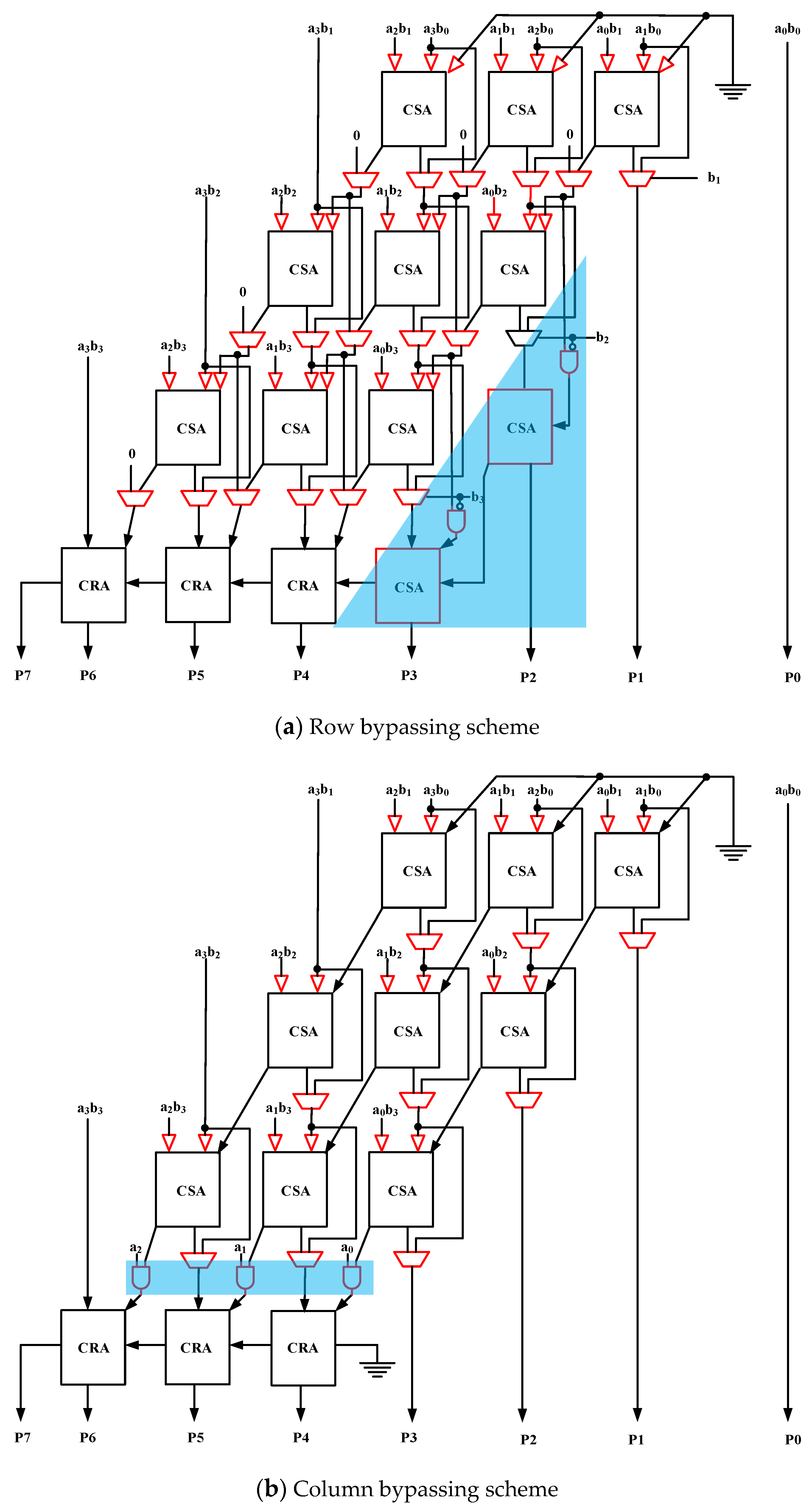
11] in conjunction with an input operands interchange scheme. The schematic of a multiplier with row bypassing scheme is illustrated in
Figure 1a. The input tri-state buffers (colored red) serve as input data signal gating when bypassing holds. The multiplexers are used to select between the full adder design output and the bypass signal. As shown in
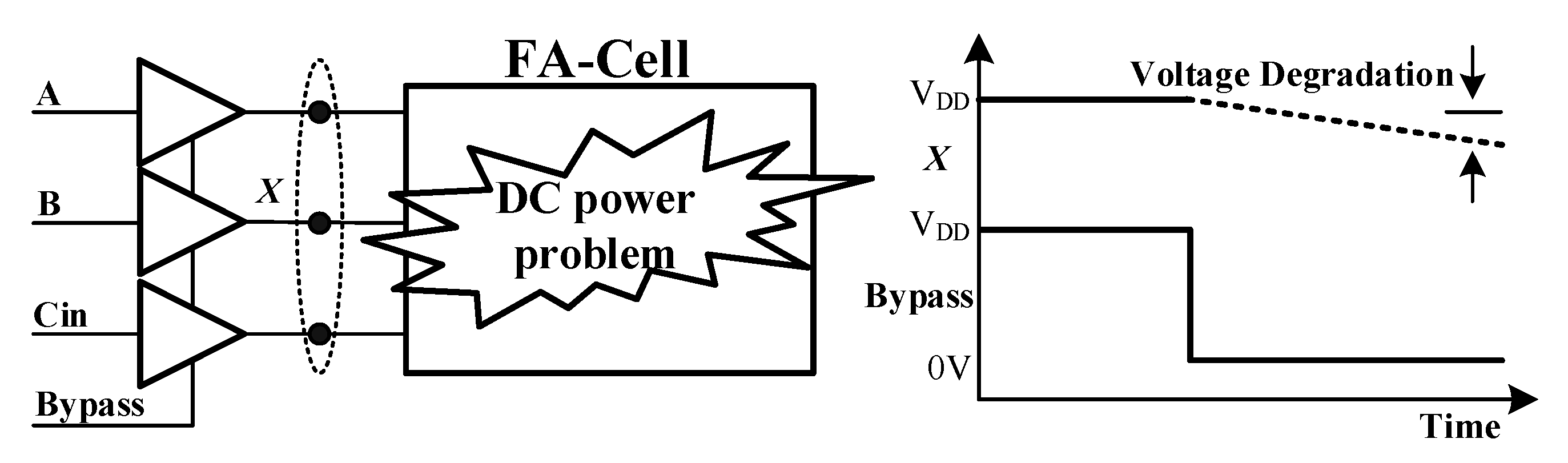
Figure 2, the main drawback of such an implementation is the voltage degradation at the floating tri-state output. The phenomenon is particularly prominent when working in lower operation frequency and/or standby mode. The degraded signals may cause both P- and N-logics to be turned on simultaneously resulting in static power dissipation. An alternative to row bypassing is column bypassing was introduced in [
10]. The corresponding multiplier schematic is given in
Figure 1b. The idea comes from the observation that when a multiplicand bit is zero; all full adder designs along the corresponding diagonal (column) will have “Cin” and the sum and input equal zero. The third input is then bypassed to the “Sum” output. Additionally, the “Cin” inputs to the carry propagation adder at the bottom of the array multiplier are always zero when column bypassing holds and are therefore, quickly evaluated by ANDing with the multiplicand bit. Note that, the blue block shown in
Figure 1 is the extra compensating circuit for ensuring the stability for multiplier [
10,
11,
12,
13,
14,
15,
16].
In [
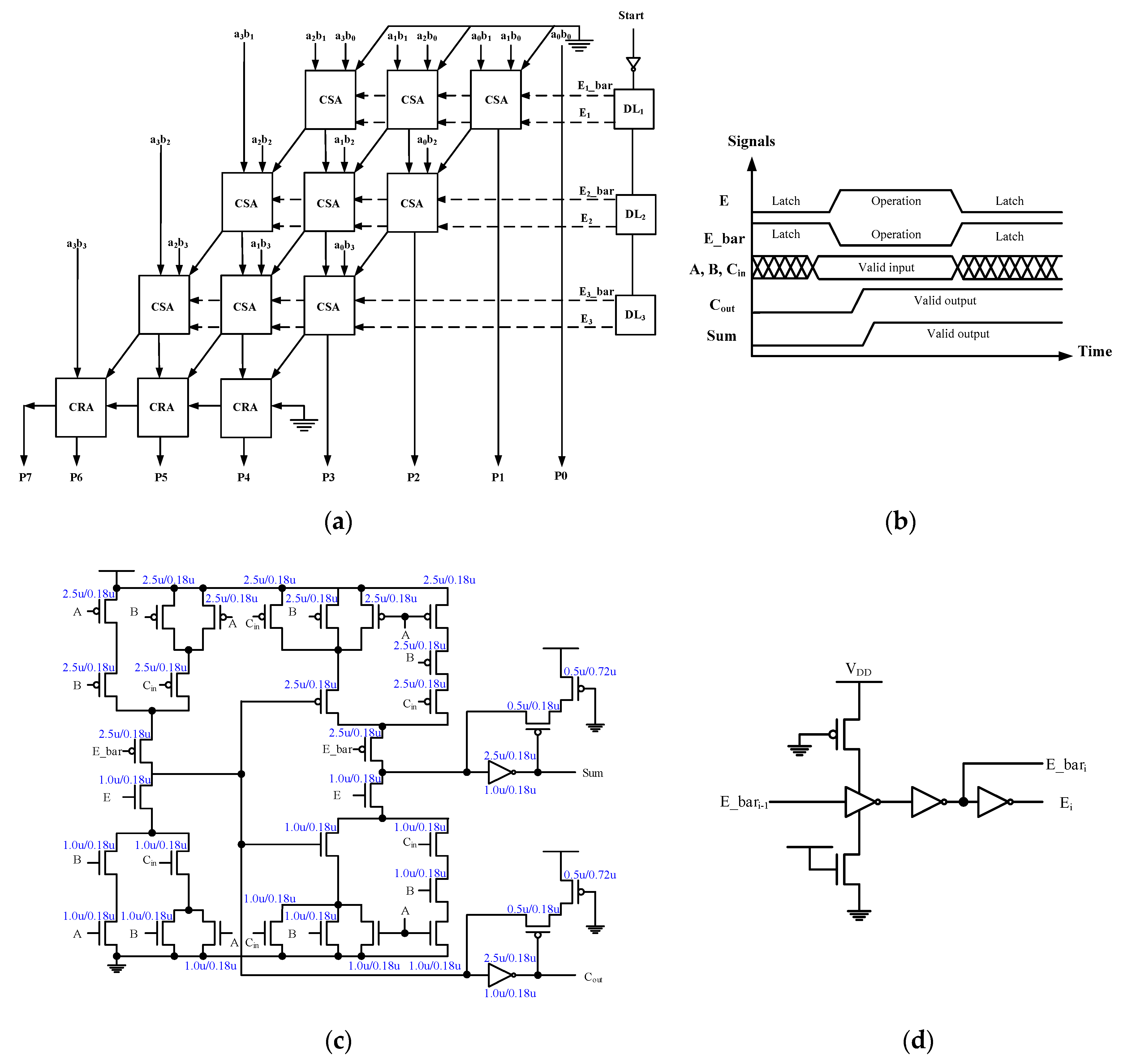
12], the partial products are latched to synchronize the input signal transition from one adder row to another in a predetermined chronological sequence. This requires carefully calibrated delay cells to synchronize the operation. As shown in
Figure 3, the basic latch-adder cell is a C
2MOS version 28 T adder design plus two keeper circuits to hold the values of “Sum” and “Cout”. Complementary enable signals “E” and “E_bar” control the timing of adder outputs. This approach observes the data flow and can further reduce the spurious signal transitions in the sum logic. The synchronization measure requires carefully calibrated delay cells to ensure correct timing as shown in
Figure 3b. The power overhead of the incurred control logic must be confined so as not to offset the power saving from synchronized operations. In general, the circuit overhead of the bypassing scheme based multiplier design is higher than the latch-adder based approach. This overhead is mainly attributed to the selection logic needed for signal bypassing [
14]. The bypassing scheme, however, does not require the elaborate transistor size tweaking needed in other delay sensitive schemes.
In this paper, we will present a novel latch-adder based low voltage and low power multiplier design for applications requiring low working frequencies (no more than 1 MHz). Due to the delay cell circuit, the proposed design is also realized by using full adder. Therefore, there is no need to adjust the transistor sizes of the delay cell circuit deliberately to extend the delay and ensure its low power consumption works efficiency.
2. Proposed Design
Based on the initial work presented in [
12], a refined latch-adder based multiplier design is developed.
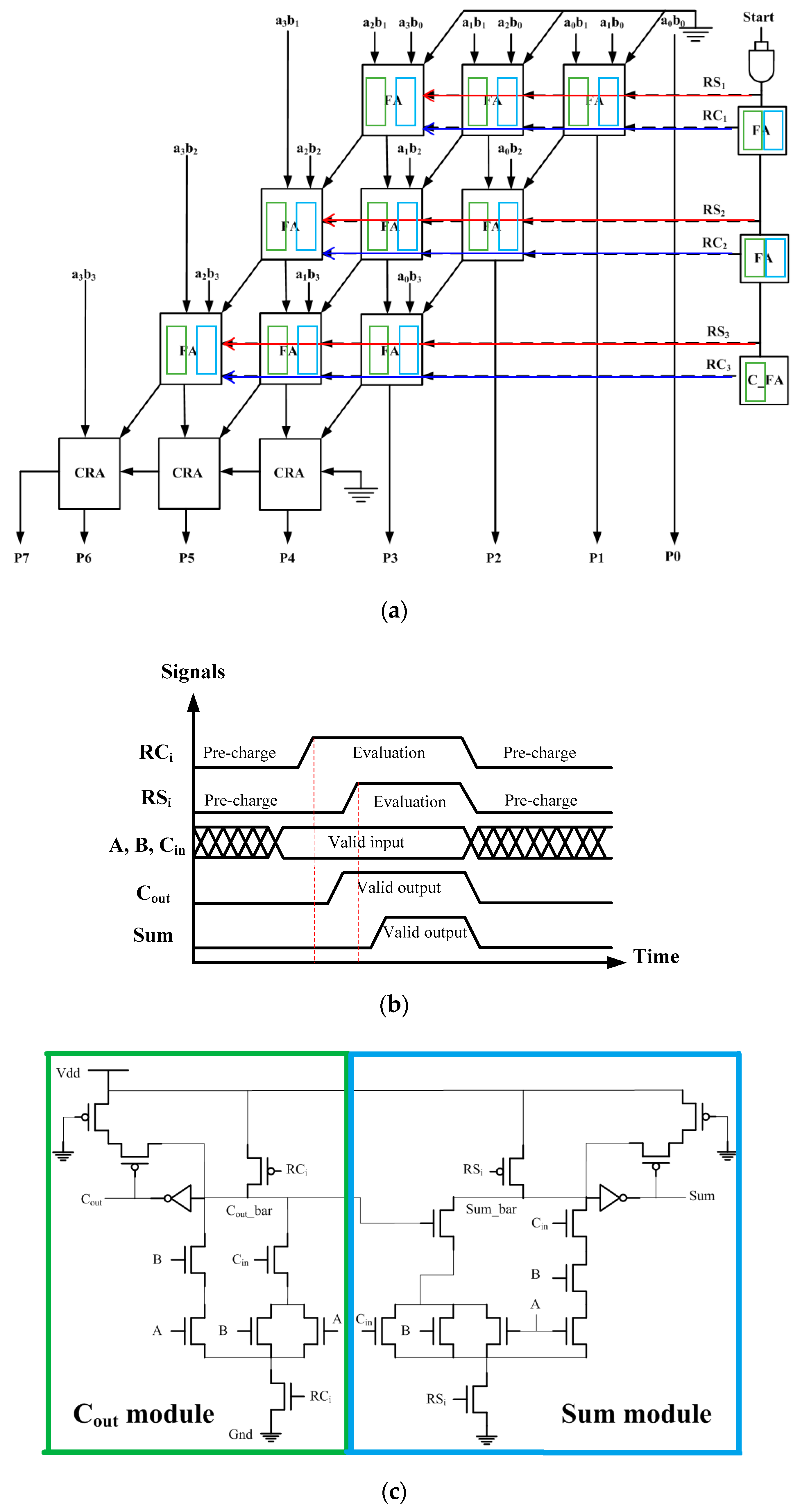
Figure 4a shows the array structure of the proposed design. Structurally, it consists of carry save adder array followed by a carry propagation adder, a chain of delay cells, and a latch control signal generator. (For simplicity, the partial product generation logic is not shown.) The signal and latch control timings are shown in
Figure 4b. RCi and RSi are latch signals which carry logic and sum logic circuits in its row of the adder array, respectively. They also serve as the control signals to strobe the operations of carry logic and sum logic circuits. The delay discrepancy in sum and carry paths within a full adder is taken into account so that the evaluation phase of the sum logic falls slightly behind that of the carry logic.
In
Figure 4, a typical 1-bit full adder design generates a “Cout” signal first, which is then fed to the sum logic circuit, is shown. In order to avoid spurious signal transition at the sum logic, when “Cout” is not ready it is necessary to delay the operation of a sum calculation. Due to the carry save scheme, all adders in the same row operate concurrently and then pass the result to the adders in the following row. This suggests a progressive style of evaluation from row to row.
To simplify the circuit of control signal generation, the latch control signal applied to the sum logic is also applied to the carry logic in the next row (RSi = RCi + 1). In other words, the operations of the sum and carry logics are time skewed in the same row but in two adjacent rows. Based on this structure, we then work on the basic adder cell with embedded latch function (or latch-adder in short). Recall that the latch-adder cell shown in
Figure 3 is realized in the C
2MOS version 28 T adder design with two additional keeper circuits to hold the values of “Sum” and “Cout”. A total of 40 MOS transistors are needed, twelve of which arise from the latch control. This extra circuit overhead is considerable as is the power consumption of the design.
In view of the described circuit issues, the proposed design adopts a semi-dynamic circuit design, i.e., dynamic full adder plus static keeper where the latch control signals RCi and RSi originate from the delay cell. The design of the proposed latch-adder cell is shown in
Figure 4c. The bulky pull-up pMOS logic for sum and carry path are each replaced by one pre-charge pMOS transistor. When the latch control signal and the pre-charge signal of the dynamic circuit are low, the logic is pre-charged to high. When the control signal turns low, the logic is evaluated by performing a conditional discharge. Two simple state keeper logics are placed at the output nodes as data latches. They can also resolve the charge sharing problem common in dynamic circuits. Alternatively, the inverter of the state keeper logic leads to a domino logic like design. When signals “Sum” and “Cout” are fed to the following row, the property of low-to-high only transitions ensures that no incorrect discharge at the beginning of the evaluation phase will occur.
Note that the output of the carry logic is also fed internally to the sum logic within the same adder cell without going through an inverter. However, the deliberate time skew between their latch control signals ensure the correct operations of the two directly connected dynamic circuits. Compared with previous latch-adder cell based designs [
12,
13], the proposed design also uses latch-adder as delay cell circuits. For this reason, it is unnecessary to adjust the transistor sizes of the delay cell circuit to lengthen the delay (the same-sized carry module and sum module designs are used in both adder cell and delay cell). Note that the delay circuit used in [
12] is a 4-transistor C
2MOS inverter and one more inverter per row is needed to generate complementary control signals as shown in
Figure 3.
3. Simulation and Measurement Results
To evaluate the power saving merits of the proposed design, 5 multiplier designs are included for comparison. These include a conventional array multiplier design using typical 28T full adder cells, a latch-adder based multiplier designs given in [
12], two bypassing scheme based multipliers presented in [
9,
10], and the proposed work. The layouts of these designs were developed first, with post layout simulations conducted to obtain results for comparison. Considering the simulation condition will largely affect the evaluation results, it is determined based on our target applications. As previously mentioned, our focus was IoT applications with relaxed speed but critical power constraints. The sampling frequency of environment data, (such as temperature and humidity), is usually below 1 MHz. The power consumption, nonetheless, is crucial to battery life time. Rather than relying on expensive state-of-the-art process technology for low power operations, the selected technology was the TSMC 180 nm CMOS process. The working frequency was selected as 1 MHz and the V
DD was set to 0.6 V.
Two 1-bit latch-adders simulation results are listed in
Table 1 to show the performance edge of the proposed design when compared with design [
12]. By interpreting the post-layout simulation results, we concluded that, the proposed design is 28.9% faster in operational speed, 11.5% lower in power consumption, and 37% improvement in the PDP index when compared with design [
12]. As previously mentioned, the delay cell of the proposed design is also optimized for timing (used adder as delay cell) to ensure that sufficient delay is reserved for the readiness of input signals.
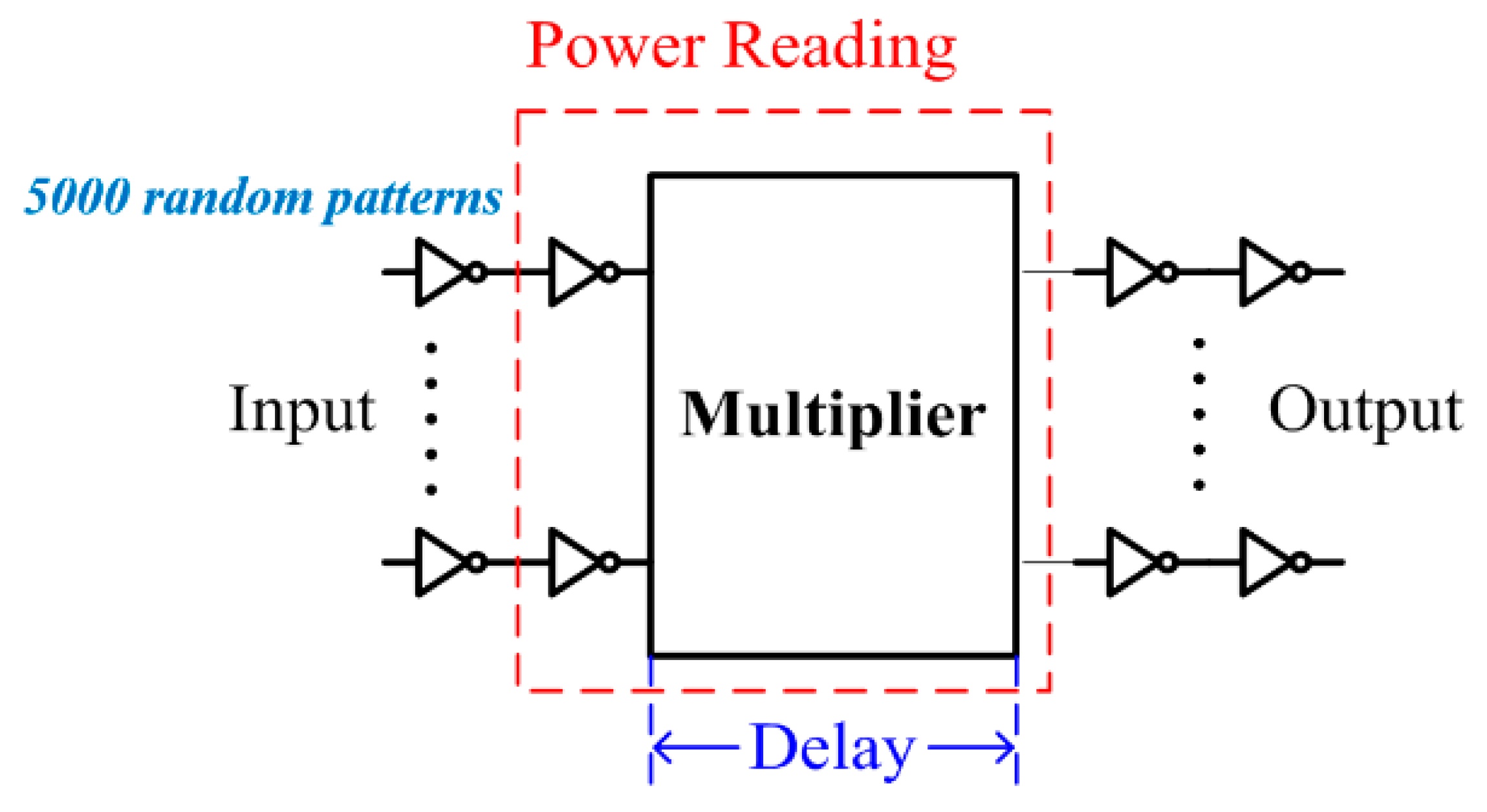
A total of 5000 test patterns are generated randomly with equal probability of zeros and ones. All nMOS/pMOS transistors were of size 1.0 um/2.5 um, except the transistors of keeper logic and delay circuits (design [
12]). The circuit arrangement is depicted in
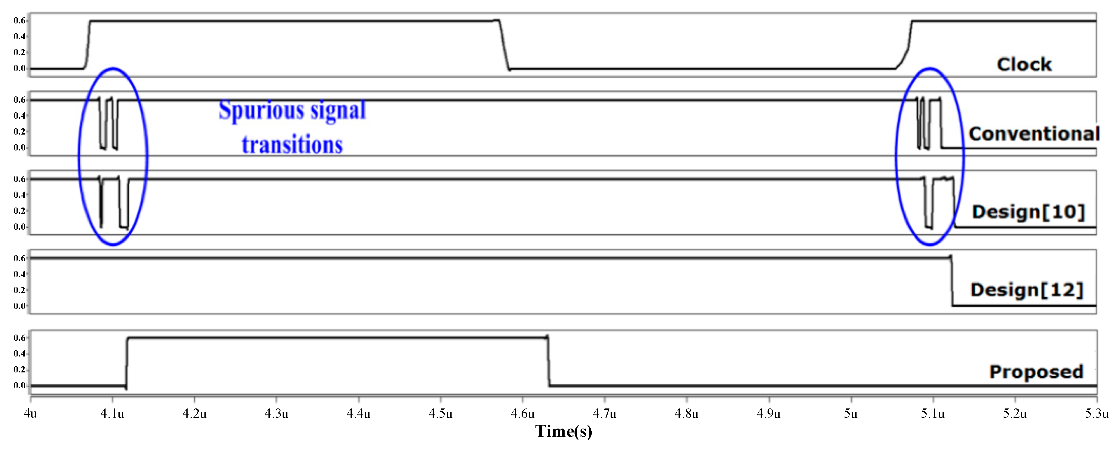
Figure 5. The simulation waveforms were first examined to illustrate the suppression of spurious signal transitions of the proposed design. In
Figure 6, the snapshot of waveforms for consecutive multiplications in four designs is given. The first row is the clock signal where one multiplication is performed in each clock cycle. The same internal node from each design are sampled and shown. We clearly observe that the conventional design and design [
10], (using a column bypassing scheme), exhibit many more signal transitions than the other latch adder based designs. Such glitches correspond to futile transitions which are detrimental to power performance. Design [
12], and the proposed design, both adopt a delay-controlled evaluation strategy and encounter no glitches at all. In addition, the proposed design employs a semi-dynamic logic structure to further reduce layout size. When the clock is zero, the output nodes of the full adder are pre-charged to zero. Although this requires extra pre-charge power, the dynamic power consumption is reduced overall because the entire P-logic is replaced by a small pre-charge transistor, greatly reducing the capacitive load.
Table 2 gives the post-layout simulation results of 8 × 8 multiplier design under the setting of (0.6 V, 1 MHz).
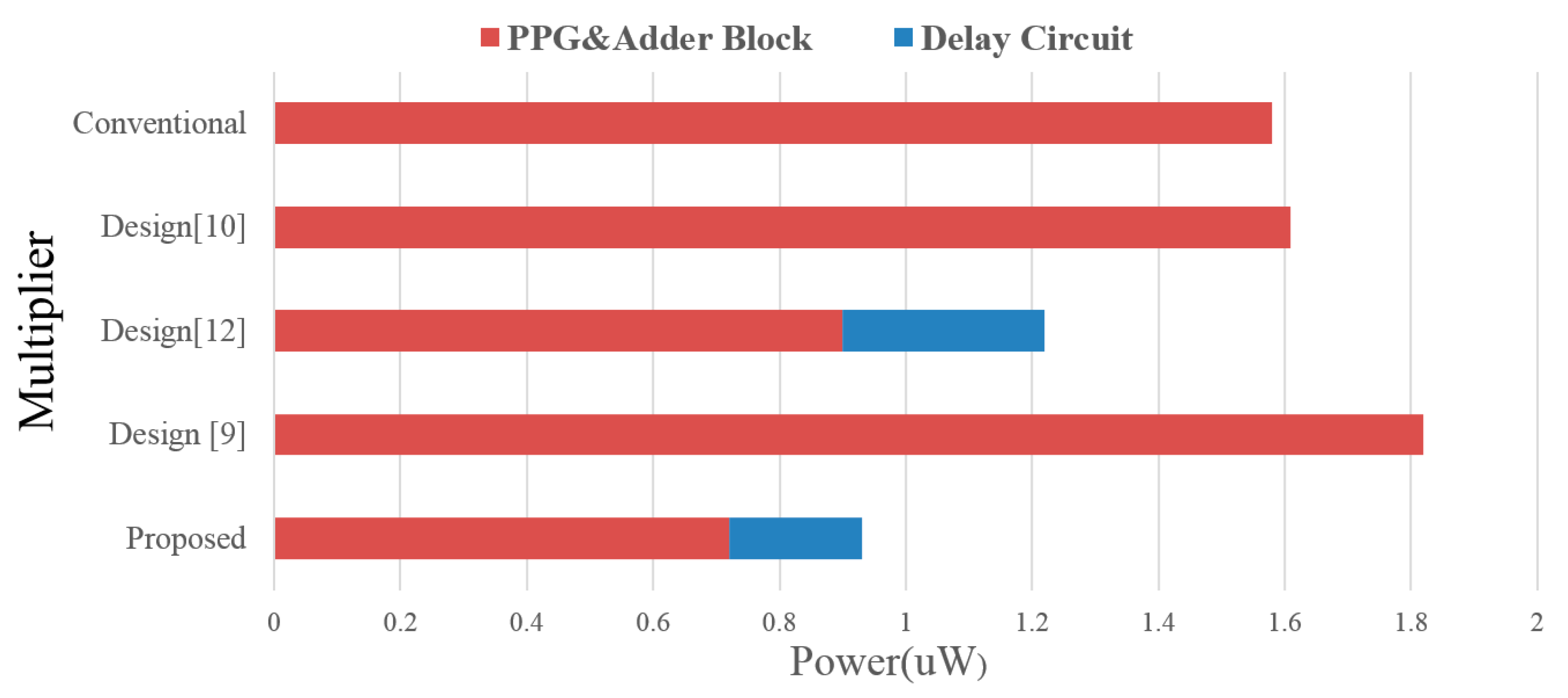
Figure 7 shows a breakdown of power consumption for all multipliers. The power consumption is divided into two parts, one for the delay line/control signal generation and the other one for the array multiplier itself. In both delay line controlled multiplier designs, the power consumption overheads of the delay line and control signal generation range from 21–26%. The power savings in the array multipliers, however, are significant and the overall power consumptions are better than the other designs. Compared with the conventional design, the saving is up to 38.6%. Design [
12] trails the proposed work and is ranked in the second place. Note that the power performance of design [
9,
10] using a row and column bypassing scheme are inferior to the conventional array multiplier design without using any power saving technique. This is because the adder inputs are gated by tri-state buffers which become floating when bypassing holds. The voltage degradation due to leakage current can be large when the working frequency is lower. This leads to larger DC power consumption in the adder cell. If the circuit is in standby mode, the effect of leakage power consumption will become even more prominent. This adverse effect can be somewhat alleviated at higher frequency operations. However, the overall power saving behavior remains inferior to our designs.
In addition to power performance, delay times to obtain valid multiplication results are also recorded. The conventional design leads in this performance index, followed by the proposed designs, and design [
12]. The fully complementary logic structure of the 28 T full adder used in the conventional design gives it the speed edge in low V
DD operations. The proposed design, however, exhibits sufficient speed performance for the target applications. Finally, a compound performance index of power consumption and speed, the power delay product, is included in the comparison. The proposed design scores highest indicating well-balanced designs for both power and speed.
Table 2 shows the layout areas of these designs. They are used to illustrate circuit complexity. The proposed design has the smallest layout areas, which are smaller than the conventional design without employing any extra circuit for latch and delay cells. We can attribute this factor to the semi-dynamic logic structure, which largely simplifies the circuit complexity of the basic adder cell. Design [
9,
10] and design [
12] all require larger layout areas than the conventional design.
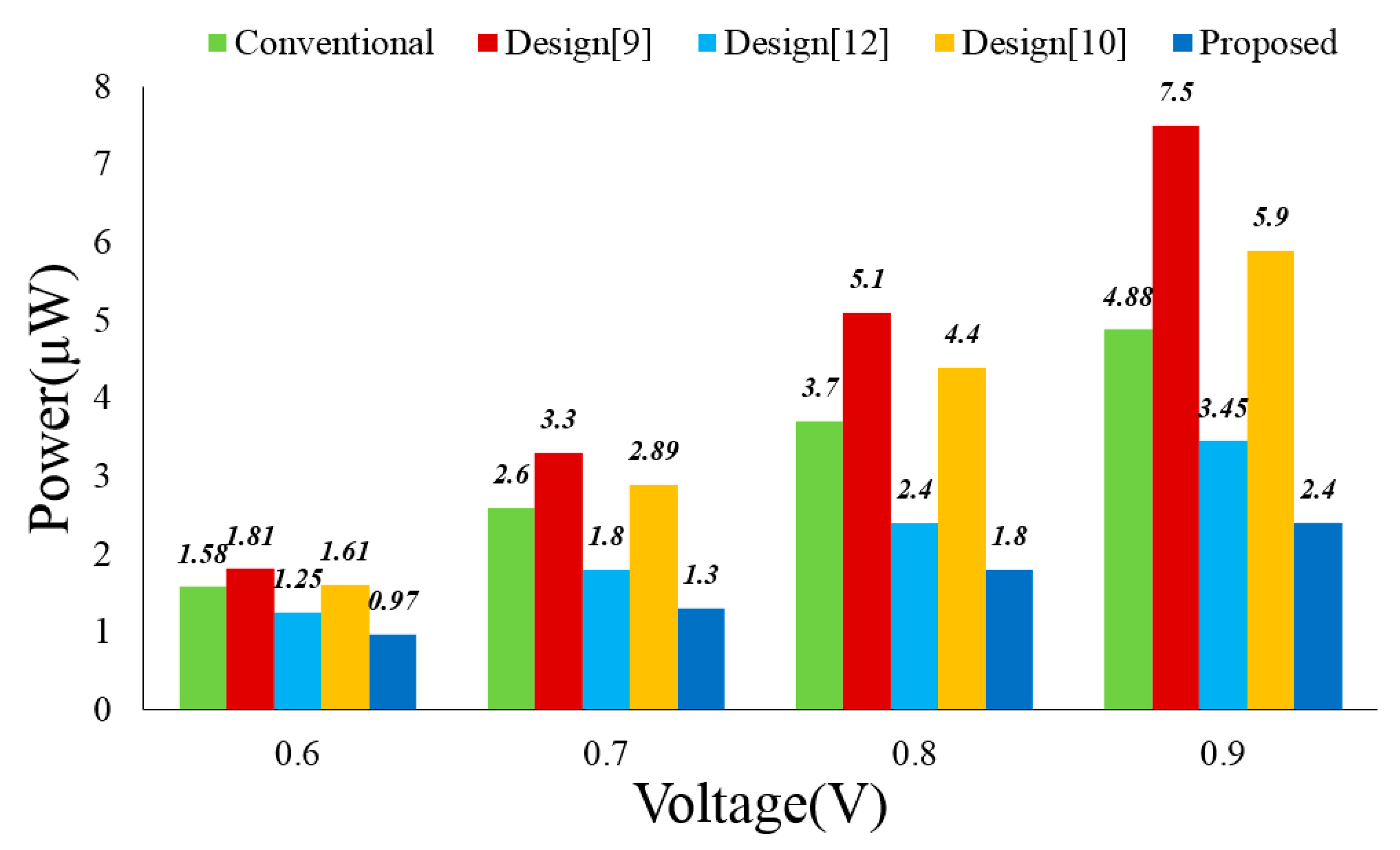
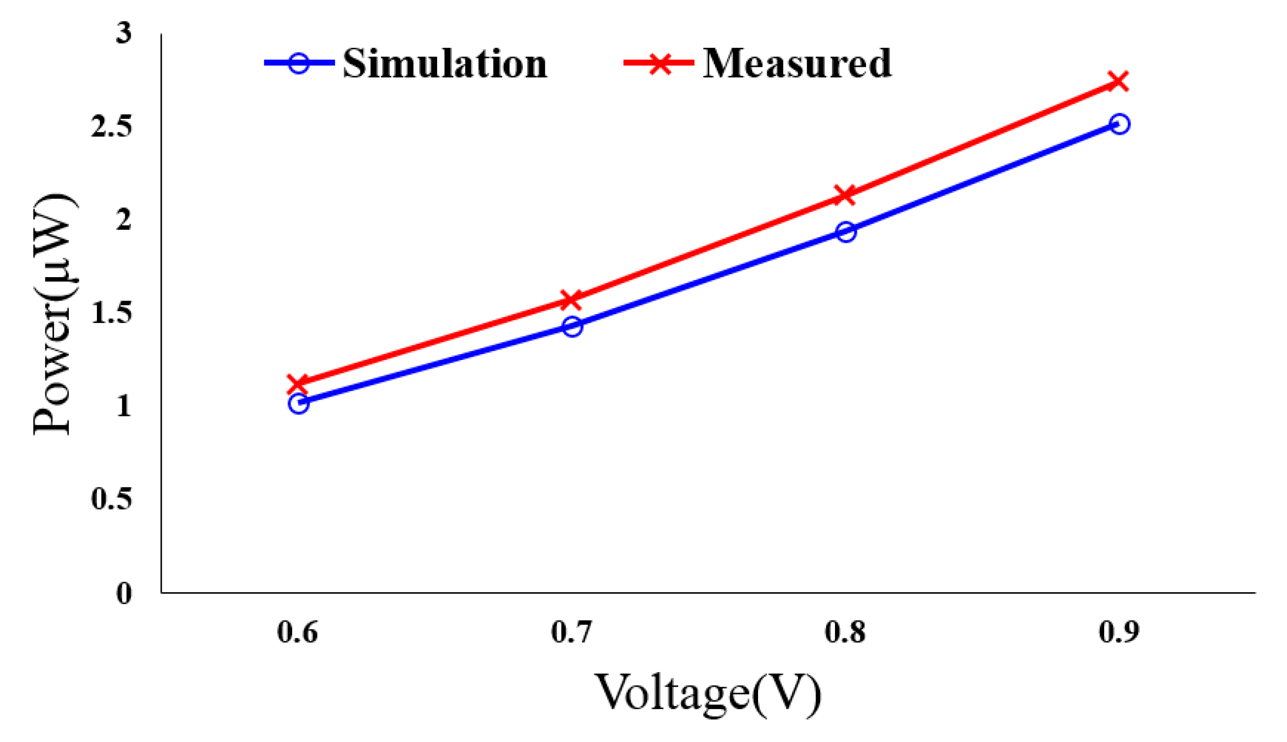
Figure 8 displays the power consumptions of these multiplier designs under different V
DD values (The working frequency remains as 1 MHz). Our design displays the least power consumption in all settings. The power consumption saving against other designs increases with the V
DD value.
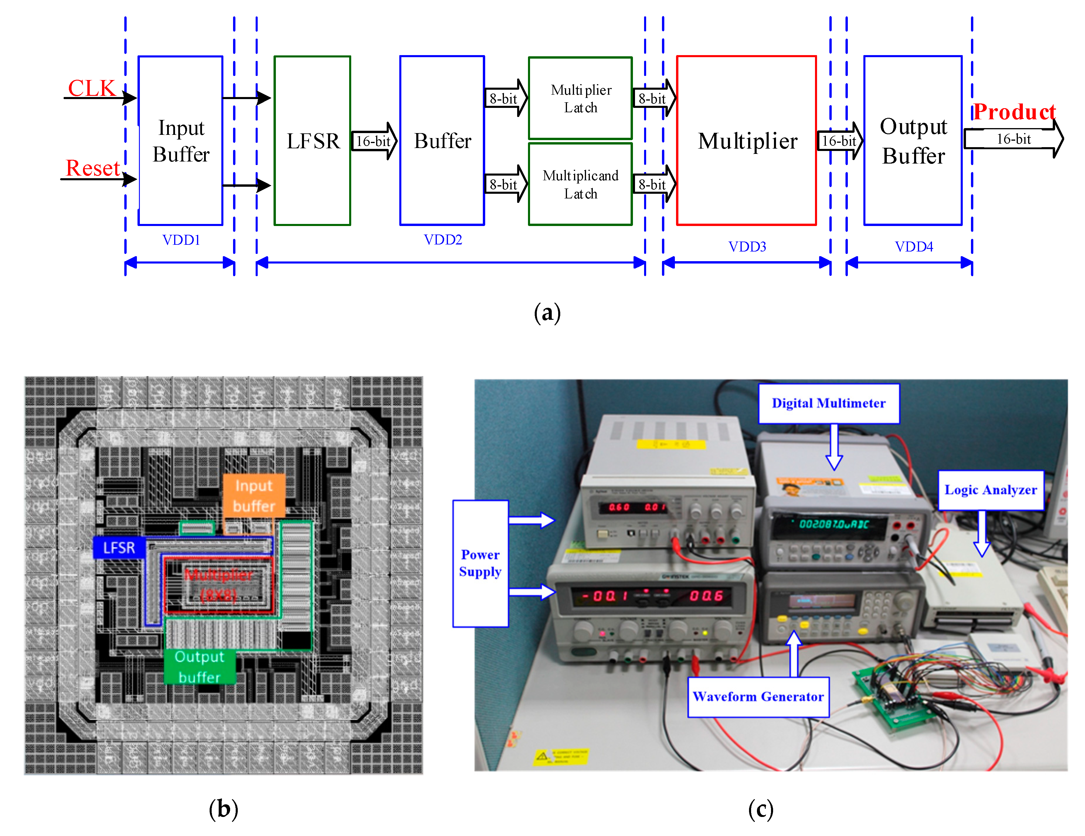
The proposed latch-adder based low power multiplier was designed and fabricated using TSMC-180 nm CMOS technology. It contains an 8 × 8 multiplier kernel and a 16-bit linear feedback shift register (LFSR) as a built-in test pattern generator. As illustrated in
Figure 9a, the input clock signal will go through input buffer and then pass to a LFSR design. This circuit provides a random pattern for the proposed multiplier design to measure the average power consumption. In order to acquire a better result, the 16-bit signal (generated by LFSR) goes through the following buffers and latches to confirm the test multiplier’s input signals can be simultaneous. The detailed chip layout schematic is shown in
Figure 9. The overall chip size is 1.02 × 1.02 mm
2. The size of the proposed multiplier design kernel circuit is only 0.33 × 0.24 mm
2 of chip area. The test platform used is shown in
Figure 9c and combines a signal generator (Agilent-33250A), logic analyzer (Acute-LA2164P), oscilloscope (Agilent MSO-X 3204A), digital current meter (Agilent-34410A), and two power supplies (Agilent-E3610A).
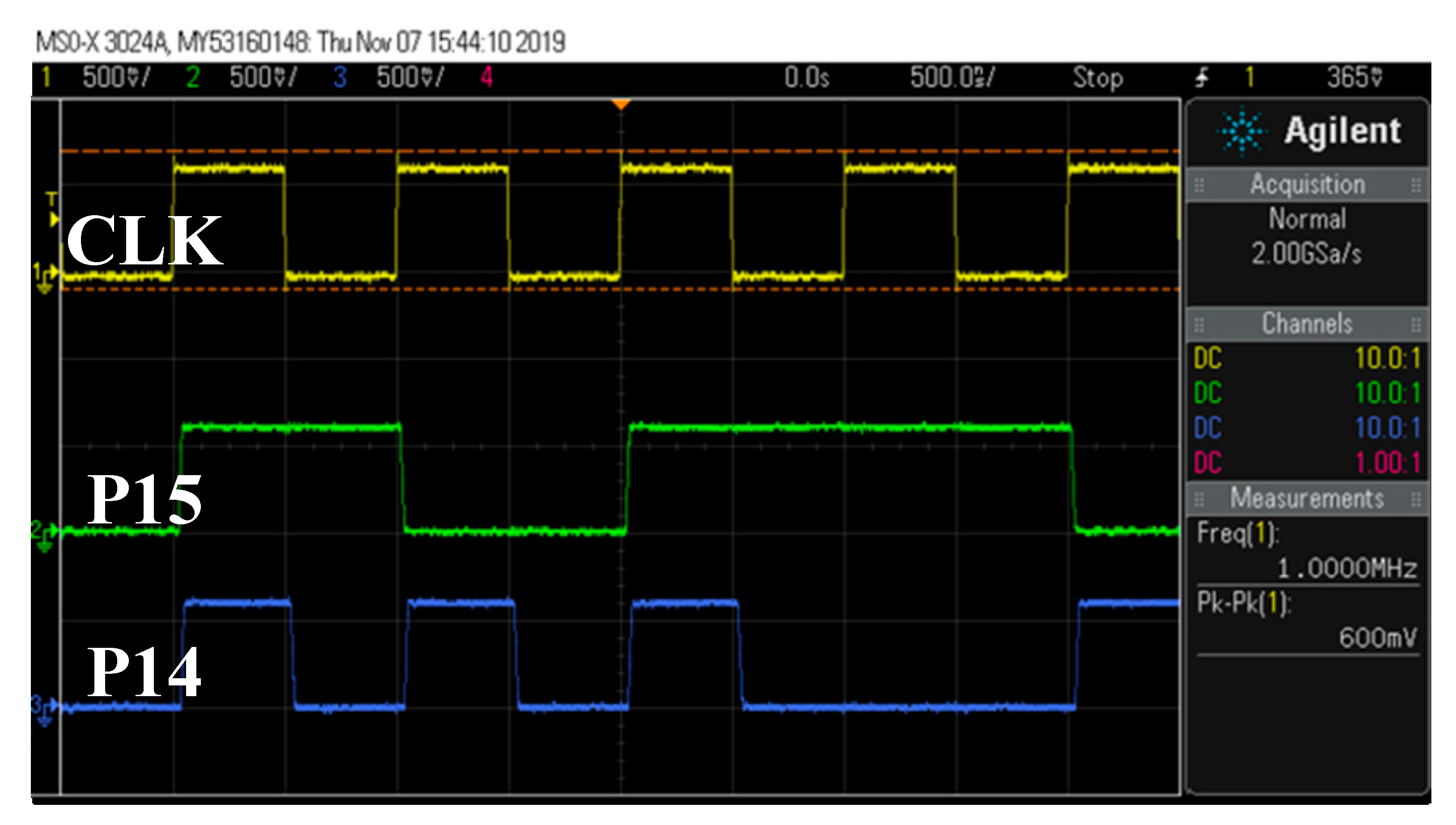
Figure 10 shows measurement waveforms of the proposed design. Each signal from up to down is input clock signal, the output signal P14, and the P15 (product). The maximum working frequency (f
max) is also measured. When V
DD equals 0.6 V, f
max is 11.7 MHz, which is over 11 times the target working frequency. This number is very close to the simulated 13.5 MHz shown in
Table 2. For V
DD settings ranging from 0.6 V to 0.9 V, the power consumptions at the target 1 MHz working frequency are shown in
Figure 11. The post layout simulation results are also included for comparison. After adding the essential measure auxiliary circuit, (including parasitic), and I/O pads, the measured power consumptions are about 10.5–11.2% higher than the post-layout simulation results. With the design running at 500 KHz, the required V
DD value of proposed low power multiplier can be reduced to 0.41 V, and the power consumption is only 427 nW.


