Article

Improved Synchronized Space Vector PWM Strategy for Three-Level Inverter at Low Modulation Index

1
School of Electrical Engineering and Automation, Tiangong University, Tianjin 300387, China
2
School of Artificial Intelligence, Tiangong University, Tianjin 300387, China
*
Author to whom correspondence should be addressed.
Electronics 2019, 8(12), 1400; https://doi.org/10.3390/electronics8121400
Submission received: 16 October 2019 / Revised: 15 November 2019 / Accepted: 21 November 2019 / Published: 23 November 2019
(This article belongs to the Special Issue Multilevel Converters)

Abstract

:
Aimed at reducing the switching loss and common-mode voltage amplitude of high-power medium-voltage three-level inverter under low modulation index conditions, an improved synchronous space vector PWM strategy is proposed in this paper. The switching times in each fundamental period are reduced by the re-division of small regions and the full use of the redundant switching state. The sum of switching algebra is introduced as an evaluation index and the switching state with the minimum value of the sum of switching algebra are adopted. Then, the common mode voltage amplitude is reduced. The theoretical analysis and experimental results show that the improved modulation strategy proposed in this paper can effectively reduce the switching loss and common-mode voltage amplitude of the inverter under the condition of the low modulation index. Moreover, the neutral-point voltage ripple is also reduced simultaneously.

1. Introduction

Compared with the traditional two-level converter, the multi-level converter has numerous advantages, such as reduced total harmonic distortion (THD), low dv/dt, and high inversion efficiency. It is widely used in wind power generation, ship propulsion, locomotive traction, and other applications [1,2,3]. When applied to the above medium-voltage high power motor system, the switching loss becomes the major component of system losses. Taking the traction drive motor system as an example, due to the poor working environment, the cooling condition is poor. Therefore, due to the limitation of heat dissipation, the switching frequency of the inverter is relatively low, usually no more than 1 kHz [4]. In addition, due to the limitation of characteristics of the inverter, common mode voltage will inevitably be generated in the system. When applied to the medium-voltage high power motor system, high common mode voltage will produce large common mode current on the motor shaft, and it may even lead to the breakdown of the insulation layer and affect the service life of the motor [5]. To sum up, how to reduce the switching loss and amplitude of common mode voltage is a problem that must be considered in the high power motor system.
At present, domestic and overseas scholars have carried out extensive and in-depth research on the problems of high switching loss [6,7,8,9,10] and high common mode voltage [11,12,13,14,15] of multilevel inverters, and have made a series of achievements. In terms of switching loss reduction, in Reference [6], a closed-loop control strategy based on carrier modulation is proposed, in which the clamping region is inserted in every half fundamental period to reduce switching loss. In Reference [7], the method of reducing switching loss by inserting the clamping region is adopted from Reference [6], but on this basis, the PI (Proportional-Integral) controller is used to solve the problem of the neutral point potential shift. Under the condition of ensuring the neutral point potential balance, the clamping region is symmetrically distributed in the fundamental period, and the low-order harmonics of the inverter output are reduced. In Reference [8], the various performances of the inverter including switching loss and neutral point voltage are analyzed, the calculation complexity of the duty cycle is simplified, and the simplified model of switching loss is constructed. Through the re-distribution of redundant small vectors, the switching loss is restrained, while the neutral point voltage wave is reduced at that moment. In Reference [9], a “0-clamp” discontinuous modulation strategy is proposed. Based on the calculation method of the average error current vector, the space vector sector in the full modulation system is partitioned. The optimal clamping mode and region boundary of the output waveform quality are determined to reduce the switching loss on the basis of satisfying the high output performance of the inverter. In Reference [10], the discontinuous modulation method is also used to set the discontinuous range of phase voltage according to the load power factor, so as to realize the suppression of switching loss of the inverter under the condition of the variable load power factor.
In terms of common mode voltage suppression, in Reference [11], a method to reduce the frequency of common mode current by reducing the number of common mode voltage changes is proposed. When the switching sequence is arranged, the change times of common mode voltage can be reduced by reducing the commutation times. Compared with the traditional continuous and discontinuous modulation strategy of the three-level inverter, the THD of output current is higher because of the non-nearest three vector synthesis method. While the frequency of the common mode current is reduced, the amplitude is not suppressed. With the decrease of the modulation index, the common mode voltage will gradually increase, and the amplitude of the common mode current will also increase. In order to suppress the common mode voltage, a modulation strategy of eliminating the common mode voltage by using the method of three zero common mode voltage vector synthesis is proposed in Reference [12]. In order to facilitate the analysis of the switch state, the multi-level inverter is equivalent to the two-level inverter in the reference. Based on the modeling of the switching loss, the lowest switching mode can be selected. But due to the degree of freedom used in the switching state setting of the strategy, the THD of the output current and voltage of the inverter is greatly increased compared to the traditional strategy. In Reference [13], considering the shortcomings of the three zero common mode voltage vector in the output waveform quality of the inverter, a modulation strategy for improving the output waveform quality is proposed based on the degree of freedom set for the switching state, but the principle of the three zero common mode voltage vector must be satisfied. Additionally, the design and selection rules of the optimal switch sequence are obtained through the analysis of the current ripple. Based on the analysis of Reference [13], Reference [14] proposes a double zero vector synthesis sequence method, which can reduce the output current ripple while ensuring the zero common mode voltage amplitude of the inverter. In Reference [15], a method of reducing switching loss by adjusting the position of the zero vector in the sampling period is proposed, and the basic vector synthesis switching sequence with small common mode voltage amplitude is selected. However, the calculation process of this method is complex, and the strategy is essentially a continuous modulation strategy, the switching loss can be further reduced. However, it must be noted that References [12,13,14,15] all adopt the synthesis method of the non-nearest three vector, the ripple, and THD value of output waveform of the inverter will go up, especially in the low modulation index.
The improved modulation strategy of the above reference can only be applied to the asynchronous modulation mode with a high carrier ratio. When the carrier ratio decreased, due to the limitation of switching frequency of the inverter, the common mode voltage amplitude can still be reduced, but the quality of output waveform will be seriously reduced. When the switching frequency is further reduced, a synchronous modulation strategy is needed to ensure the synchronization and symmetry of the output phase voltage waveform of the inverter [16,17,18,19,20]. In Reference [18], the synchronous space vector modulation is introduced into the three-level inverter for the first time, and the modulation strategy under the condition of different parity of the reference vector number is designed. In Reference [19], a multi-mode synchronous SVPWM (Space Vector Pulse Width Modulation) strategy with low switching frequency is proposed. By designing the switching sequence, the output waveform quality of the inverter is improved in the full modulation system. In Reference [20], four kinds of synchronous discontinuous space vector modulation strategies are proposed. Through four different phase voltage clamping methods, the output waveform quality of the converter is guaranteed and the switching loss is reduced. However, there are some problems in the strategy, such as large switching loss and high amplitude of common mode voltage, which need to be improved.
This paper presents a synchronous space vector modulation strategy that can reduce the switching loss and common mode voltage amplitude simultaneously at low switching frequency. Aiming at the switching loss and common mode voltage amplitude suppression, a new switching sequence design method is proposed based on the traditional switching sequence design rules. By using the redundant switching state of the three-level inverter space voltage vector, an improved modulation strategy is formed to achieve the simultaneous suppression of the switching loss and common mode voltage amplitude under the low-modulation index of NPC (Neutral Point Clamped) three-level inverter.

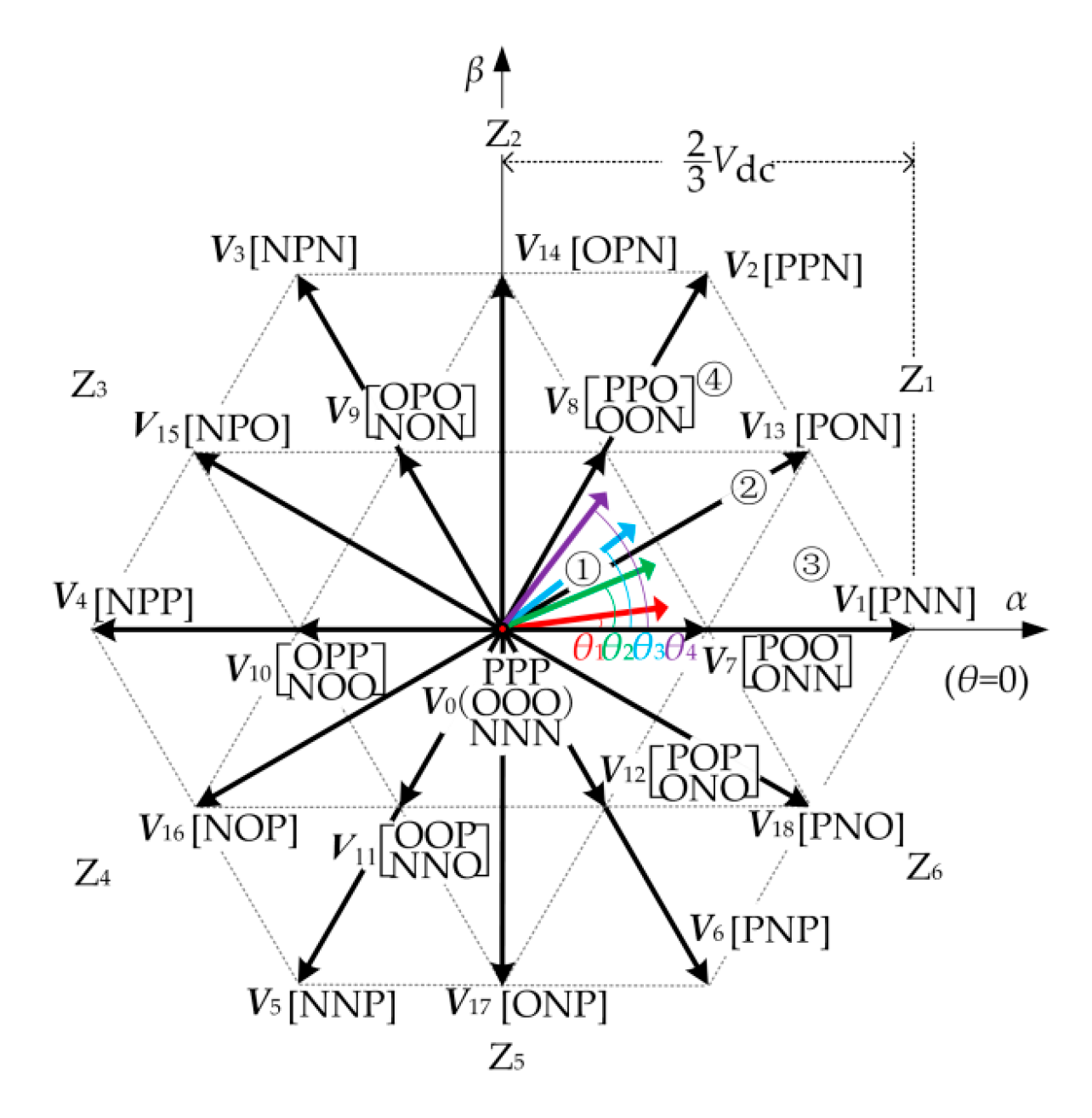
2. Space Vector Modulation of Three-Level Inverter

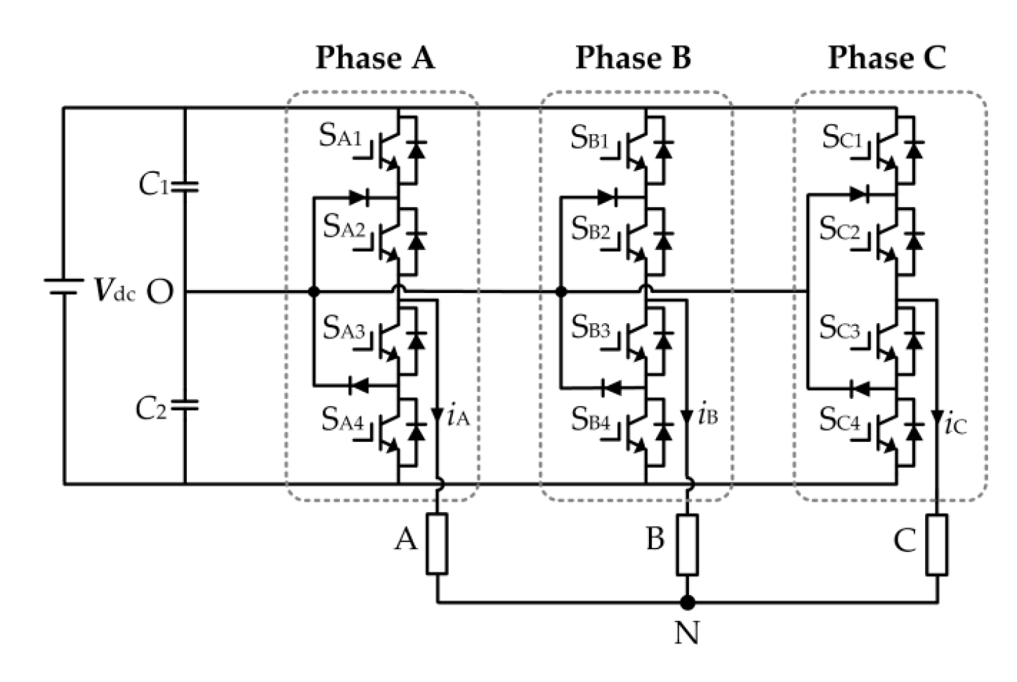
2.1. NPC Three-Level Inverter

The topology of NPC three-level inverter is shown in Figure 1.
Each phase leg has three switching states: P, O, and N. The definition is shown in Table 1. Sx1Sx4 represents the on-off state of four switches in X ∈ (A, B, C) phase, 1 represents on, and 0 represents off. There is a total of 33 = 27 switching state combinations for three-level inverters, which corresponds to 19 basic voltage vectors in the space vector diagram. As shown in Figure 2, θ is the angle between the reference vector Vref and α axis.
Basic voltage vectors can be divided into four categories (one zero vector, six small vectors, six medium vectors, and six large vectors) according to their magnitudes. Each small vector corresponds to two switching state combinations and the zero vector corresponds to three switching state combinations. The whole space vector diagram can be divided into six sectors Z1–Z6 and each sector can be further divided into four small regions, as shown in Figure 2. In conventional synchronous space vector modulation strategies, the reference vector Vref is synthesized by the nearest three basic vectors.
Modulation index m is defined as:
m = 3 V ref V dc
where Vref is the amplitude of the reference vector. Taking Vref in region ① of sector Z1 as an example, Vref is synthesized by the basic vector V7, V8, and V0. The dwell time of each basic vector can be calculated according to the principle of volt-second balance.
{ V ref T s = V 7 T 1 + V 8 T 2 + V 0 T 0 T s = T 1 + T 2 + T 0
where Ts is the sampling period, T1, T2, and T0 are the dwell times of basic vectors V7, V8, and V0, respectively.

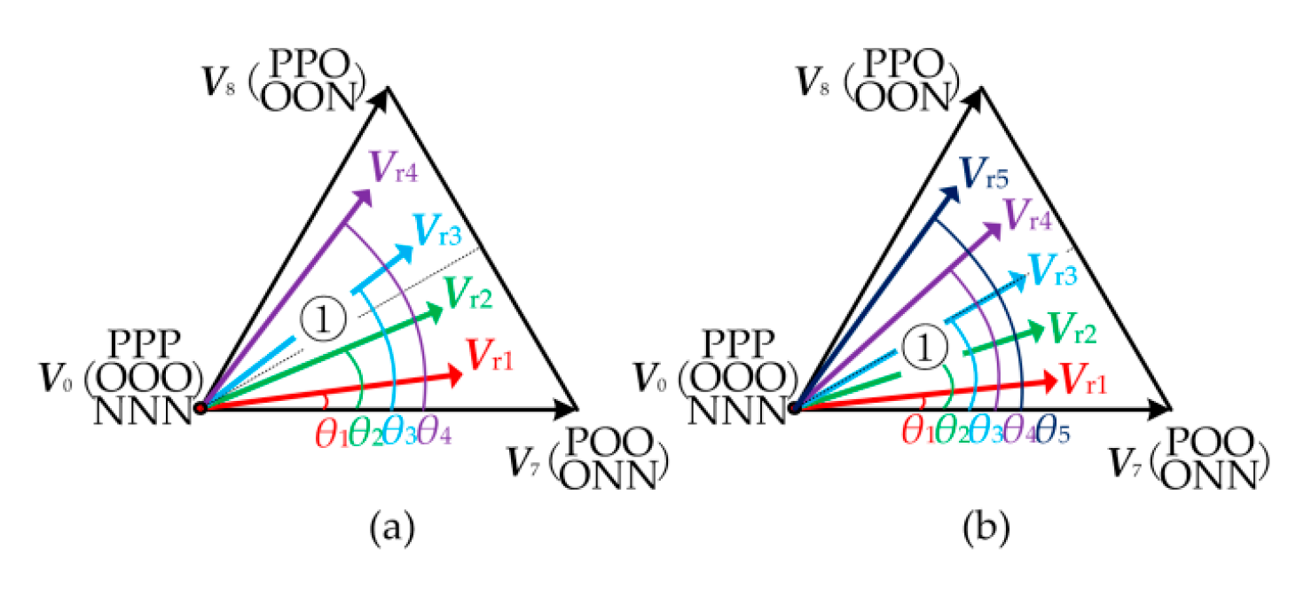
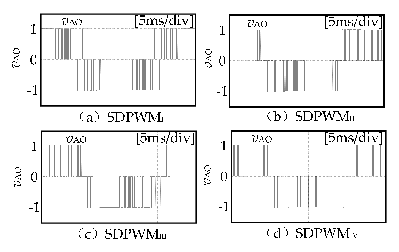
2.2. Traditional Synchronized Discontinuous Space Vector Modulation Strategy

In synchronous space vector modulation strategies, reference vectors need to be evenly distributed in the space vector diagram. If the number of reference vectors N is odd, there will be a reference vector located at the center of each sector and the other reference vectors will be symmetrically distributed on both sides of the sector’s center. While N is even, reference vectors shall not be located at the center of each sector [18]. Taking N = 4 and N = 5 as examples, distributions of reference vectors in sector ZI are shown in Figure 3.
When the inverter is operated under low carrier ratio conditions, in order to reduce the sub-harmonics, third harmonics and even harmonics, the output voltage needs to meet the synchronization conditions:
{ v AO ( θ ± 2 π ) = v AO ( θ ) v BO ( θ ± 2 π ) = v BO ( θ ) v CO ( θ ± 2 π ) = v CO ( θ )
Three-phase symmetry conditions:
v AO ( θ ) = v BO ( θ + 2 3 π ) = v CO ( θ 2 3 π )
Half-wave symmetry conditions:
{ v AO ( θ ± π ) = v AO ( θ ) v BO ( θ ± π ) = v BO ( θ ) v CO ( θ ± π ) = v CO ( θ )
Constrained by the above synchronization and symmetry conditions, the design principles of the switching sequence can be obtained as follows [19]:
Principle 1: There will be at most two switching of any arbitrary phase leg in each sampling period.
Principle 2: At most two-phase leg has switching in each sampling period.
Principle 3: At the intersection of two sample periods, the switching between P and N is not allowed in any arbitrary phase leg.
Principle 4: The terminal state of the current sampling period is the starting state of the next sampling period.
According to the above four principles, the traditional modulation strategy can be designed. Taking N = 4 as an example, when the modulation index m ≤ 0.5043, the switching sequence of SDPWMI~SDPWMIV in sector ZI is shown in Table 2 [20].
Four clamping modes of the traditional synchronous discontinuous space vector modulation strategy are described in detail below. The A-phase voltage clamping state diagram of SDPWMI~SDPWMIV is shown in Figure 4.
It can be seen from the switching sequence of the traditional synchronous discontinuous modulation strategy, shown in Table 2, that four kinds of synchronous discontinuous modulation strategies clamp one phase, respectively. It can be seen from Table 2 and the schematic diagram that when a phase is clamped in P state within 2π/3 cycle, that is, SA1 and SA2 keep 2π/3 cycle inactive; when a phase is clamped in O state in 2π/3 period, that is, SA2 and SA3 keep 2π/3 period inactive; when a phase is clamped in N state in 2π/3 period, that is, SA3 and SA4 keep 2π/3 period inactive. In other words, four kinds of discontinuous modulation strategies clamp a certain phase with a width of 2π/3 cycle in the fundamental period. As the switching device does not act in the clamping state, the switching times are reduced in the fundamental period, and then the switching loss of the whole inverter is reduced.
Taking SDPWMII as an example, there is no switching in phase A in sector Z1, and the switching state is always P, which is defined as the clamping state P. Similarly, in SDPWMIII, there is no switching in phase C in sector Z1, and the switching state is always N, which is defined as clamping state N. It can be concluded from Table 2 that distributions of clamping states for different modulation strategies are different in each fundamental period.

3. Improved Synchronized Space Vector Modulation Strategy

3.1. Switching Frequency Reduction

3.1.1. Switching Number Analysis of Conventional Modulation Strategy

From Section 2.2, taking N = 4 as an example, when the modulation index m ≤ 0.5043, the switching times of SDPWMI~SDPWMIV in each fundamental period are 5, 5, 5, and 6, respectively.
As shown in Table 2, for SDPWMII and SDPWMIII, there is only one clamping state in each sector, and no additional switching occurs when sampling periods switch from one to another. However, at the boundary of the two sectors, additional switching is required because of the change of the clamping state (for example, when SDPWMIII switches between sector Z1 and Z2, the switching state of three-phase bridge arm needs to be changed from OON to OPO or OPN). For SDPWMI and SDPWMIV, the clamping state needs to be changed in each sector, so that there is additional switching (for example, when SDPWMI is switched from clamping state P to clamping state N, the switching state of the three-phase bridge arm is changed from POO to OON).
As shown in Figure 2, zero vector corresponds to three switching states: PPP, NNN, and OOO. Table 2 shows that PPP or NNN are adopted in SDPWMI~SDPWMIV, and OOO is not adopted. In fact, OOO can be used to design the switching sequence to further reduce the switching times of inverters.

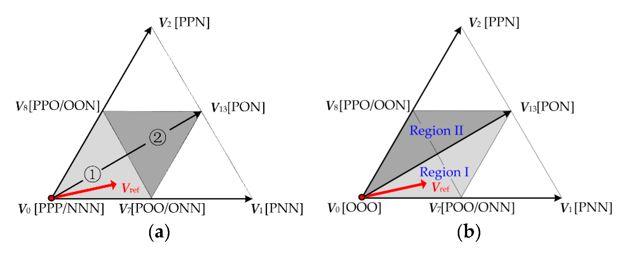
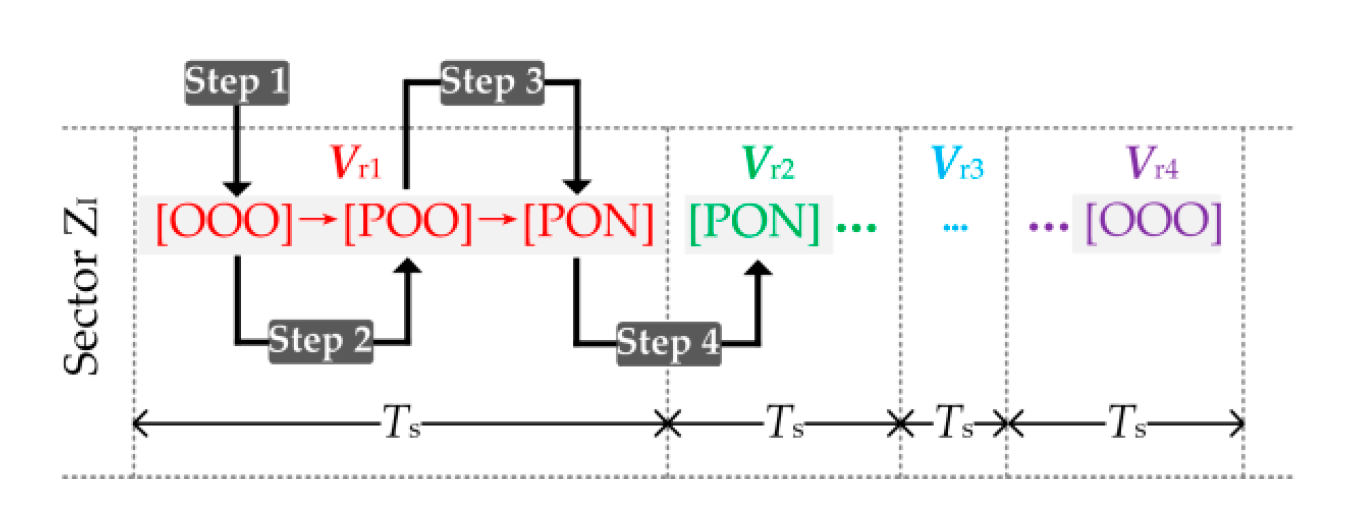
3.1.2. Improved Design Method of Switch Sequence for Modulation Strategy

In order to reduce the switching caused by the change of the clamping state, an improved design method of switching sequence is presented.
Taking region ① of sector Z1 as an example, as shown in Figure 5a, basic vectors V0, V7, and V8 are used to synthesize the reference vector for the conventional modulation method. While in region ② of sector ZI, the basic vectors V7, V8, and V13 are used to synthesize the reference vector. For the improved design method proposed in this paper, region I and region II are re-divided into region I and region II with medium vector V13 as the boundary. As shown in Figure 5b, when the reference vector is located in region I, the basic vectors V0, V7, and V13 are used. When the reference vectors are located in region II, the basic vectors V0, V8, and V13 are used to synthesize the reference vector. In order to further reduce the switching frequency of the inverter, two new principles are added based on Principles 1–4.
Principle 5: In each sampling period, the switching sequence need to start or end with the switching state corresponding to zero vectors.
Principle 6: Switching can only occur in one phase leg during each switching state alternation.
According to the parity of N, switching sequence synthesis can be divided into two modes.
Mode 1: When N is even, take sector Z1 as an example. There is no reference vector in the center of the sector. Switching sequences V0V7 (V8) ↔ V13 are used to synthesize the reference vector. The switching sequence in other sectors can be obtained in the same manner. At the intersection of the two sample periods, the switching state corresponding to zero or medium vector can be used for transition. At the boundary of the two sectors, the switching state corresponding to zero vector can be used for transition. Then, the additional switching action caused by the switching of the sample period, sector, or clamp state can be reduced.
Mode 2: When N is odd, there is a reference vector at the center of the sector, where θ = π/6. Except for the reference vector at θ = π/6, the switching sequences of other reference vectors Vr1~Vr2 and Vr4~Vr5 are the same as Mode 1, which is V0V7 (V8) ↔ V13. The sequence of the reference vector is V7 (V8) ↔ V0V8 (V7). This is because the starting/terminal switching state of Vr3 is different from the terminal/starting switching state of Vr2 and Vr4. There will be additional switching actions when the clamp state is changed, which is similar to that of conventional modulation strategies. However, compared with conventional strategies, the additional switching caused by the sector or clamp state switching can still be reduced.

3.2. Common-Mode Voltage Suppression

Common-mode voltage of the three-level inverter is defined as the voltage between load neutral point N and neutral point O of the DC-link capacitor. The relationship between the common-mode voltage and three-phase voltage can be expressed as follows:
{ v AO = L d i A dt + R i A + v CM v BO = L d i B dt + R i B + v CM v CO = L d i C dt + R i C + v CM
where L and R are load inductance and resistance, vAO, vBO, vCO, iA, iB, and iC are three-phase voltage and current, respectively, vCM is common-mode voltage. As the three-phase load is symmetrical, the sum of three-phase current is zero:
i A + i B + i C = 0
According to Formulas (6) and (7), common-mode voltage can be expressed as
v CM = v AO + v BO + v CO 3 = V dc ( S A + S B + S C ) 6
where SA, SB, and SC are three-phase switching states of the inverter. The relationship between SA, SB, SC, and the switching states of each phase switch device Sx1~Sx4 is expressed as follows:
{ S A = S A 1 + S A 2 1 S B = S B 1 + S B 2 1 S C = S C 1 + S C 2 1
K is defined as sum of switching algebra
K = | S A + S B + S C |
According to the above analysis, in order to reduce the common-mode voltage, it is necessary to select the switching state with the minimum value of K to design the switching sequence. Thus, a new principle needs to be presented.
Principle 7: Priority should be given to the switching state with the minimum value of K during the design of the switching sequence.
In summary, with Principle 1–7 as constraints, an improved modulation strategy can be designed to reduce the switching loss and common-mode voltage amplitude simultaneously. The flow chart of the design process of the switching sequence is shown in Figure 6.
From Principle 5 and 7, the starting switch state of Vr1 is OOO. From Principle 6, the next switching state of Vr1 is POO. The terminal switching state of Vr1 is PON according to the region partition shown in Figure 5b. From Principle 4, the starting switch state of Vr2 is PON, and so on. All switching sequences corresponding to Vr1~Vr4 in Z1 sector can be obtained, as shown in Table 3. Table 3 shows that there is no switching action in phase B and phase B is always clamped to switching state O.

4. Switching Loss and Common Mode Voltage Amplitude Analysis

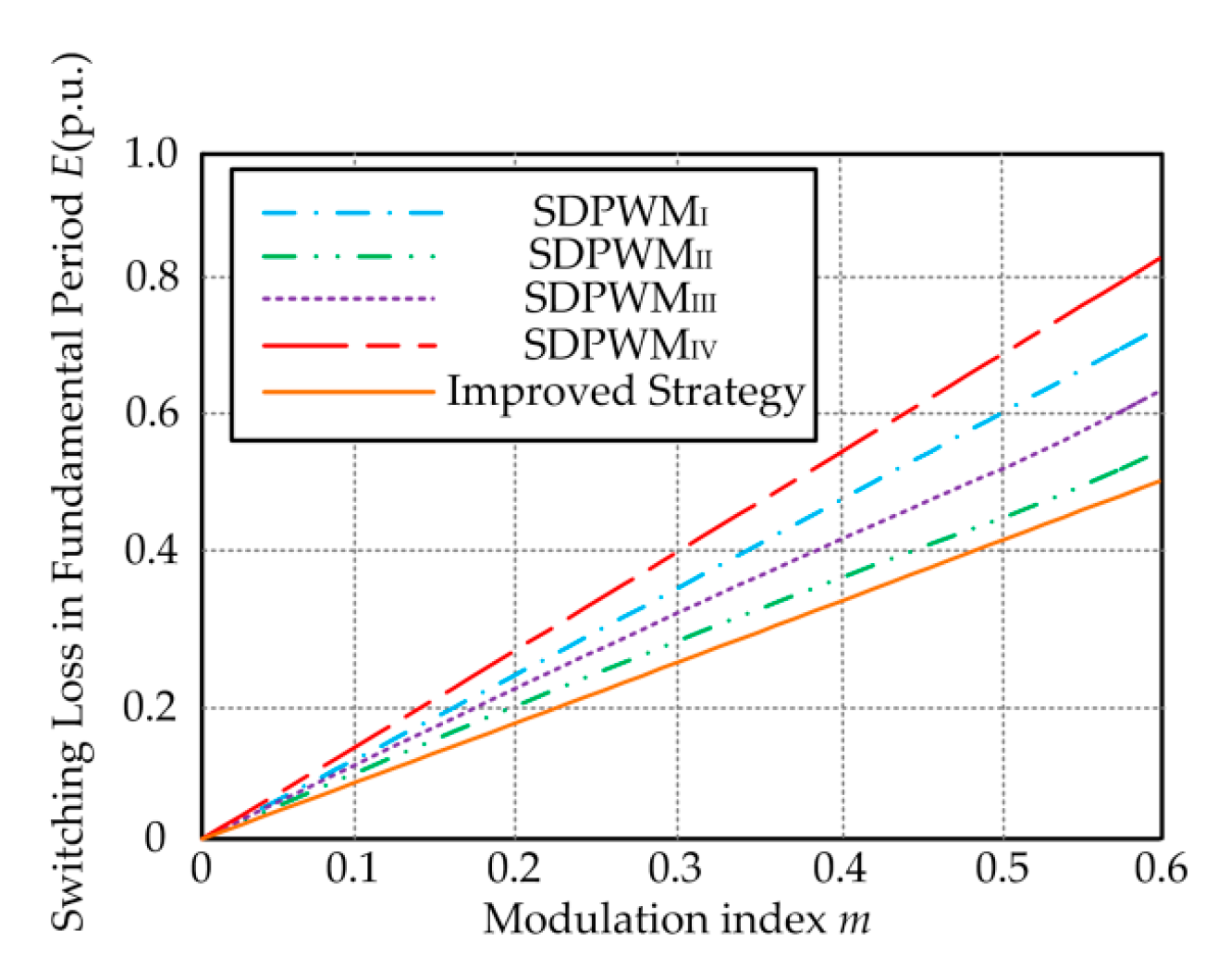
4.1. Switching Loss Analysis

The power device used in the experiment is Infineon F3L100R07W2E3_B11 series IGBT. According to the datasSheet and the switching sequences of different modulation strategies, the expression of the switching loss can be obtained (11).
E = 3 m [ j = 2 , 4 , 6 , 8 , 10 E on ( | I cos ( θ 1 _ j φ ) | ) + j = 1 , 3 , 5 , 7 , 9 E off ( | I cos ( θ 1 _ j φ ) | ) + k = 2 , 4 , 6 , 8 , 10 E on ( | I cos ( θ 2 _ k φ ) | ) + k = 1 , 3 , 5 , 7 , 9 E off ( | I cos ( θ 2 _ k φ ) | ) ]
where I is the rms value of phase current, θi_j is the switching angle (0 < θi_j < 2π), i is the order of the switches, j and k are the order of the switching angle of each switch, φ is the power factor angle, and −π/2 < φ < π/2. Since both SDPWMI~SDPWMIV and the modulation strategies proposed in this paper satisfy half-wave symmetry or quarter-cycle symmetry, the switching angles of each modulation strategy can be translated from the values in the half-cycle or quarter-cycle to obtain the remaining switching angles in the fundamental cycle.
Taking the improved modulation strategy as an example, when N = 4, the switching angles of switches SA1 and SA2 in the first quarter of the fundamental period are shown in Table 4. According to Formula (11) and Table 4, the switching loss of the improved modulation strategy can be obtained. The switching losses of SDPWMI~SDPWMIV can also be obtained in the same manner. Taking power factor angle φ = π/4 as an example, the switching losses of different modulation strategies with the variation of the modulation index are shown in Figure 7. It shows that the switching loss of the improved modulation strategy is lower than that of the four conventional modulation strategies when 0 < m < 0.6.

4.2. Common-Mode Voltage Analysis

Taking SDPWMI and SDPWMIII as examples, the switching sequence synthesized Vr1 for SDPWMI is POO → PPO → PPP. The common-mode voltage generated by POO, PPO, and PPP are Vdc/6, Vdc/3, and Vdc/2. Thus, the common-mode voltage amplitude of sequence POO → PPO → PPP is Vdc/2. Similarly, the switching sequence synthesized Vr1 for SDPWMIII is OON-ONN-NNN, and the common-mode voltage generated by OON, ONN, and NNN are −Vdc/6, −Vdc/3, and Vdc/2. Thus, the common-mode voltage amplitude of sequence OON → ONN → NNN is Vdc/2. The common-mode voltage amplitude of SDPWMI~SDPWMIV can be deduced by the above method, and the result is Vdc/2.
For the improved modulation strategy proposed in this paper, the switching sequence OOO → POO → PON is adopted to synthesize Vr1, and the common-mode voltage generated by the OOO, POO, and PON is 0, Vdc/6, and 0, respectively. Thus, the common-mode voltage amplitude of sequence OOO → POO → PON is Vdc/6. The comparison shows that the common-mode voltage amplitude of the conventional modulation strategies is Vdc/2, and that of the improved modulation strategy is Vdc/6. The improved modulation strategy proposed in this paper effectively reduces the common-mode voltage amplitude.

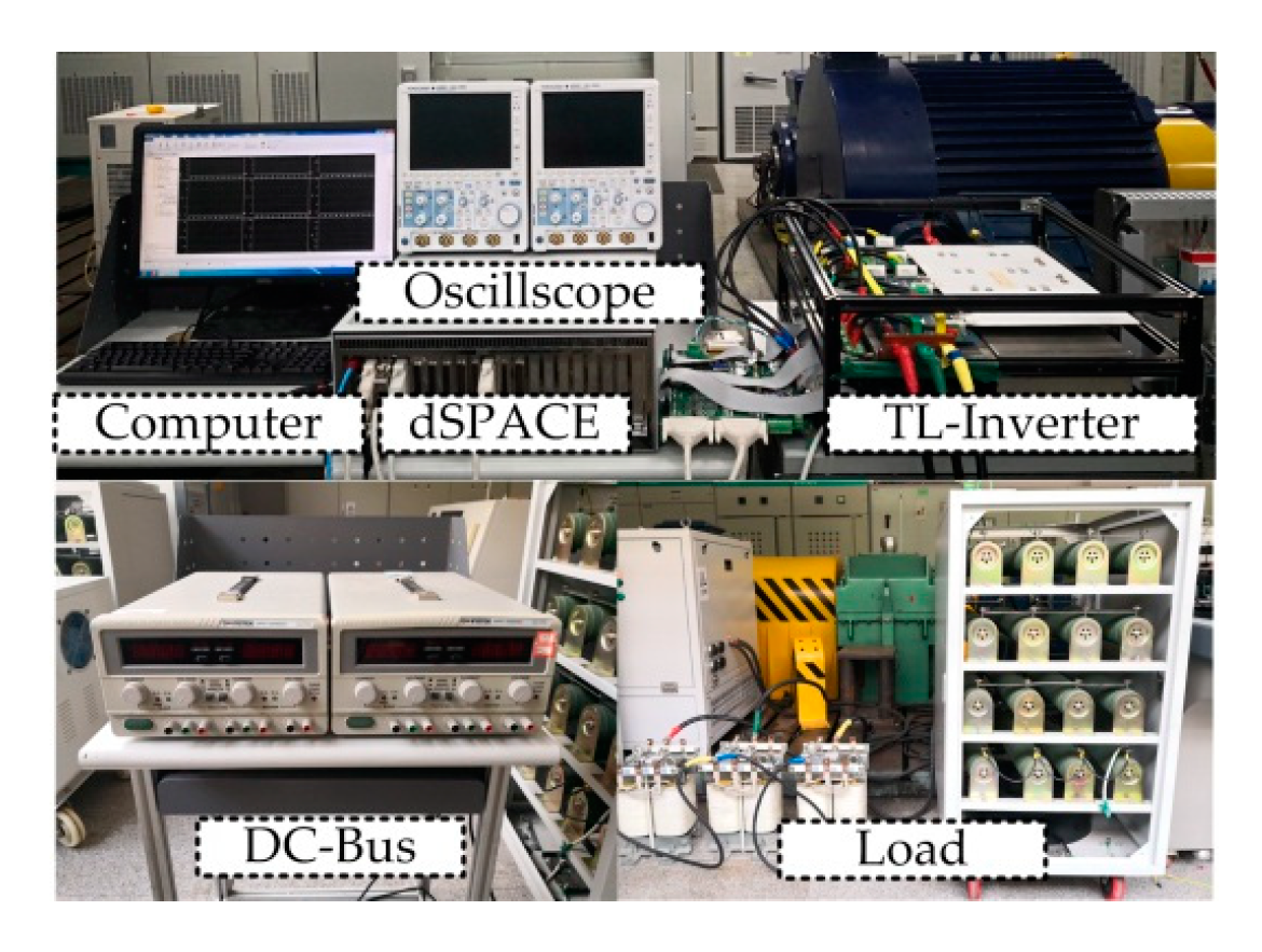
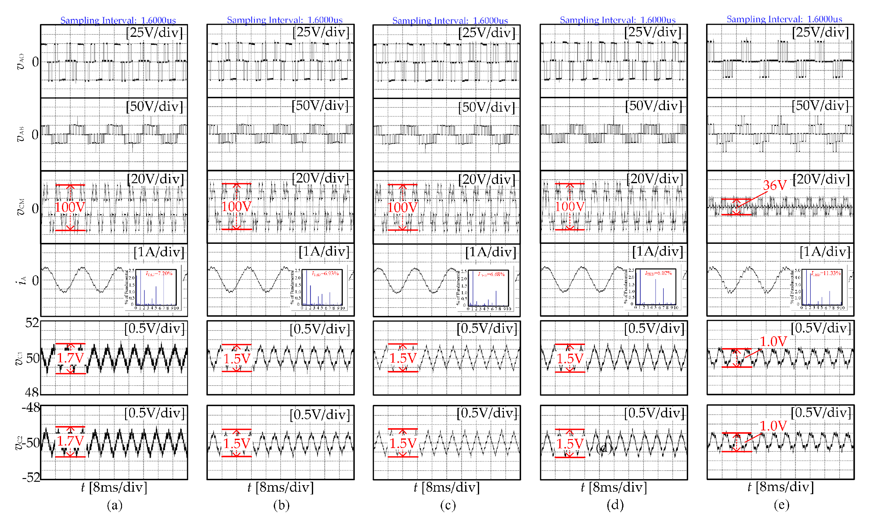
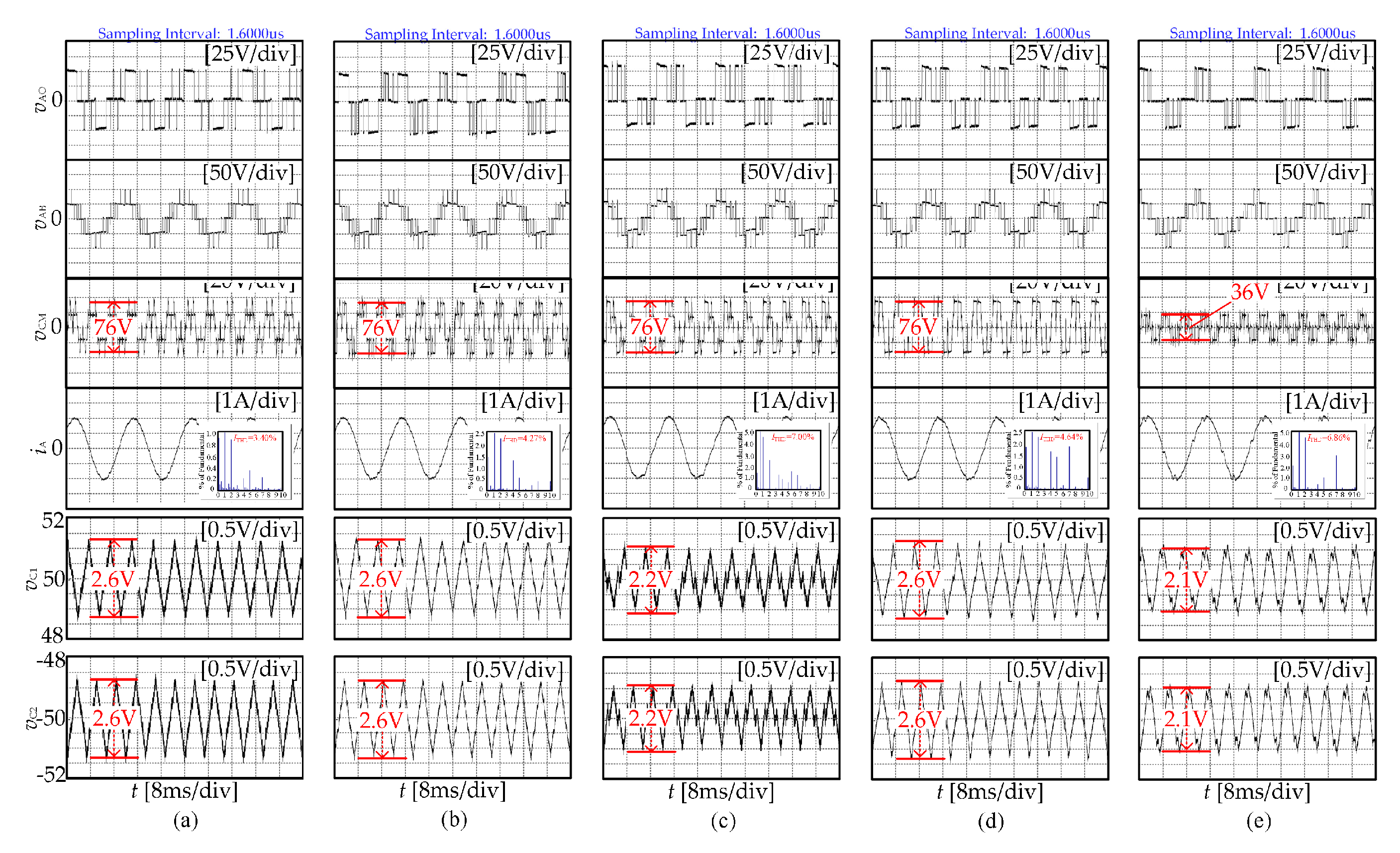
5. Analysis of Experimental Results

In order to verify the feasibility and effectiveness of the proposed strategy, dSPACE DS1007 Rapid Prototyping Development System is used as the controller and the Infineon F3L75R07W2E3_B11 IGBT module is used to compose the three-level inverter. The prototype is shown in Figure 8, and the experimental parameters are shown in Table 5.
Figure 9 and Figure 10 show the experimental waveforms of phase voltage vAO, line voltage vAB, common-mode voltage vCM, output current iA, and upper and lower capacitance voltage for SDPWMI~SDPWMIV and improved strategy (N = 4) under conditions of m = 0.4 and m = 0.6. As can be seen, compared with the four conventional synchronous discontinuous modulation strategies, when m = 0.4, the common-mode voltage amplitude of the improved strategy decreases from Vdc/2 to Vdc/6. When m = 0.6, the common-mode voltage amplitude of the improved strategy decreases from Vdc/3 to Vdc/6.
It can be seen from the voltage waveform of the upper and lower capacitors that the ripple of the neutral point voltage of the modulation strategy proposed in this paper is slightly lower than that of the traditional method. When m = 0.4, the capacitance voltage ripple is reduced from 1.5 V–1.7 V of the traditional method to 1.0 V of the proposed strategy, and when m = 0.6 the capacitance voltage ripple is reduced from 2.2 V–2.6 V of the traditional method to 2.1 V of the proposed strategy. It also can be seen that the output current waveform quality of the improved strategy is slightly lower than that of the conventional synchronous discontinuous modulation strategy, and that is because the improved strategy chooses the non-nearest three vectors to synthesize the reference vector.

6. Conclusions

In this paper, an improved synchronous discontinuous space vector modulation strategy for the NPC three-level inverter under a low modulation index condition is proposed. The modulation strategy has the following characteristics:
(1) By re-partitioning the small regions and making full use of the redundant switching state, the extra switching action during the switching between sector and clamp state is avoided. Taking N = 4 as an example, compared with SDPWMI~SDPWMIV, the improved strategy reduces switching times from five or six to four.
(2) The concept of the sum of switching algebra are introduced, and the switching states corresponding to zero and small vectors are selected according to the principle of the minimum sum of the switching algebra. Then, the common-mode voltage amplitude can be effectively reduced. Compared with SDPWMI~SDPWMIV, the common-mode voltage amplitude is reduced from Vdc/2 to Vdc/6.
The theoretical and experimental results show that the improved modulation strategy proposed in this paper can effectively reduce the switching loss and common-mode voltage amplitude of the inverter, and improve the efficiency and operational reliability of the inverter. The experimental results also verify that the modulation strategy proposed in this paper can effectively reduce the voltage ripple of the upper and lower capacitors of the NPC three-level inverter.

Author Contributions

Conceptualization, X.G. and G.Z.; methodology, B.W. and G.Z.; software, Z.W.; validation, B.W. and Z.W.; formal analysis, X.G. and W.C.; writing—original draft preparation, B.W.; writing—review and editing, Z.W. and W.C.; funding acquisition, X.G. and G.Z.

Funding

This research was funded by “The Natural Science Foundation of Tianjin, grant number 19JCYBJC21800”, “The National Natural Science Foundation of China, grant number 51807140” and “Tianjin College Innovation Team Training program of China, grant number TD13-5039”.

Conflicts of Interest

The authors declare no conflict of interest.

References

  1. Zhang, G.; Wei, B.; Gu, X.; Li, X.; Zhou, Z.; Chen, W. Sector Subdivision Based SVPWM Strategy of Neutral-Point-Clamped Three-Level Inverter for Current Ripple Reduction. Energies 2019, 12, 2734. [Google Scholar] [CrossRef]
  2. Mukherjee, S.; Santu, K.G.; Banerjee, S.A. Flexible Discontinuous Modulation Scheme With Hybrid Capacitor Voltage Balancing Strategy for Three-Level NPC Traction Inverter. IEEE Trans. Ind. Electron. 2019, 66, 3333–3343. [Google Scholar] [CrossRef]
  3. Zhang, Y.; Bai, Y.; Yang, H.; Zhang, B. Low Switching Frequency Model Predictive Control of Three-Level Inverter-Fed IM Drives With Speed-Sensorless and Field-Weakening Operations. IEEE Trans. Ind. Electron. 2019, 66, 4262–4272. [Google Scholar] [CrossRef]
  4. Rathore, A.K.; Holtz, J.; Boller, T. Synchronous Optimal Pulse width Modulation for Low-Switching-Frequency Control of Medium-Voltage Multilevel Inverters. IEEE Trans. Ind. Electron. 2010, 57, 2374–2381. [Google Scholar] [CrossRef]
  5. Kumar, P.R.; Rajeevan, P.P.; Mathew, K.; Gopakumar, K.; Leon, J.I.; Franquelo, L.G. A Three-Level Common-Mode Voltage Eliminated Inverter With Single DC Supply Using Flying Capacitor Inverter and Cascaded H-Bridge. IEEE Trans. Power Electron. 2014, 29, 1402–1409. [Google Scholar] [CrossRef]
  6. Chaturvedi, P.K.; Jain, S.; Agarwal, P. Reduced switching loss pulse width modulation technique for three-level diode clamped inverter. IET Power Electron. 2011, 4, 393–399. [Google Scholar] [CrossRef]
  7. Chaturvedi, P.; Jain, S.; Agarwal, P. Carrier-Based Neutral Point Potential Regulator With Reduced Switching Losses for Three-Level Diode-Clamped Inverter. IEEE Trans. Ind. Electron. 2014, 61, 613–624. [Google Scholar] [CrossRef]
  8. Jiao, Y.; Lee, F.C.; Lu, S.Z. Space vector modulation for three-level NPC inverter with neutral point voltage balance and switching loss reduction. IEEE Trans. Power Electron. 2014, 29, 5579–5591. [Google Scholar] [CrossRef]
  9. Xia, C.; Zhang, G.; Yan, Y. Discontinuous Space Vector PWM Strategy of Neutral-Point-Clamped Three-Level Inverters for Output Current Ripple Reduction. IEEE Trans. Power Electron. 2017, 32, 5109–5121. [Google Scholar] [CrossRef]
  10. Mukherjee, S.; Giri, S.K.; Kundu, S.; Banerjee, S. A Generalized Discontinuous PWM Scheme for Three-Level NPC Traction Inverter With Minimum Switching Loss for Electric Vehicles. IEEE Trans. Ind. Appl. 2019, 55, 516–528. [Google Scholar] [CrossRef]
  11. Videt, A.; Le Moigne, P.; Idir, N.; Baudesson, P.; Cimetiere, X. A New Carrier-Based PWM Providing Common-Mode-Current Reduction and DC-Bus Balancing for Three-Level Inverters. IEEE Trans. Ind. Electron. 2007, 54, 3001–3011. [Google Scholar] [CrossRef]
  12. Nguyen, N.V.; Nguyen, T.-K.T.; Lee, H.-H. A reduced switching loss PWM strategy to eliminate common-mode voltage in multilevel inverters. IEEE Trans. Power Electron. 2015, 30, 5425–5438. [Google Scholar] [CrossRef]
  13. Nguyen, T.K.T.; Nguyen, N.V.; Prasad, N.R. Eliminated Common-Mode Voltage Pulse width Modulation to Reduce Output Current Ripple for Multilevel Inverters. IEEE Trans. Power Electron. 2016, 31, 5952–5966. [Google Scholar] [CrossRef]
  14. Nguyen, T.K.T.; Nguyen, N.V.; Novel Prasad, N.R. Eliminated Common-Mode Voltage PWM Sequences and an Online Algorithm to Reduce Current Ripple for a Three-Level Inverter. IEEE Trans. Power Electron. 2017, 32, 7482–7493. [Google Scholar] [CrossRef]
  15. Xing, X.; Li, X.; Gao, F. Improved Space Vector Modulation Technique for Neutral-Point Voltage Oscillation and Common-Mode Voltage Reduction in Three-Level Inverter. IEEE Trans. Power Electron. 2019, 34, 8697–8714. [Google Scholar] [CrossRef]
  16. Narayanan, G.; Ranganathan, V.T. Synchronised PWM strategies based on space vector approach.Part 1: Principles of waveform generation. IEE Proc. Electr. Power Appl. 1999, 146, 267–275. [Google Scholar] [CrossRef]
  17. Beig, A.R. Synchronized SVPWM Algorithm for the Over-modulation Region of a Low Switching Frequency Medium-Voltage Three-Level VSI. IEEE Trans. Ind. Electron. 2012, 59, 4545–4554. [Google Scholar] [CrossRef]
  18. Beig, A.R.; Narayanan, G.; Ranganathan, V.T. Modified SVPWM Algorithm for Three Level VSI With Synchronized and Symmetrical Waveforms. IEEE Trans. Ind. Electron. 2007, 54, 486–494. [Google Scholar] [CrossRef]
  19. Chen, W.; Sun, H.; Gu, X.; Xia, C. Synchronized Space-Vector PWM for Three-Level VSI With Lower Harmonic Distortion and Switching Frequency. IEEE Trans. Power Electron. 2016, 31, 6428–6441. [Google Scholar] [CrossRef]
  20. Beig, A.R.; Kanukollu, S.; Hosani, K.A. Space-Vector-Based Synchronized Three-Level Discontinuous PWM for Medium-Voltage High-Power VSI. IEEE Trans. Ind. Electron. 2014, 61, 3891–3901. [Google Scholar] [CrossRef]
Figure 1. Topology of NPC three-level inverter.
Electronics 08 01400 g001
Figure 2. Space vector diagram of the three-level inverter.
Electronics 08 01400 g002
Figure 3. Distribution of reference vectors (a) N = 4 (b) N = 5.
Electronics 08 01400 g003
Figure 4. Clamping diagram of traditional synchronous discontinuous modulation strategy.
Electronics 08 01400 g004
Figure 5. The division of small regions in Sector Z1. (a) Conventional strategy; (b) improved strategy.
Electronics 08 01400 g005
Figure 6. Flow chart of the sequence design of the improved modulation strategy.
Electronics 08 01400 g006
Figure 7. Switching loss figure at φ = π/4.
Electronics 08 01400 g007
Figure 8. Physical figure of experimental system.
Electronics 08 01400 g008
Figure 9. Experimental waveforms of SDPWMI~SDPWMIV and the improved strategy at m = 0.4. (a) SDPWMI; (b) SDPWMII; (c) SDPWMIII; (d) SDPWMIV; and (e) improved strategy.
Electronics 08 01400 g009
Figure 10. Experimental waveforms of SDPWMI~SDPWMIV and the improved strategy at m = 0.6 (a) SDPWMI; (b) SDPWMII; (c) SDPWMIII; (d) SDPWMIV; and (e) improved strategy.
Electronics 08 01400 g010
Table 1. Contrast table of switching function and output level of the three-level inverter.
Sx1Sx2Sx3Sx4LevelStation
1100Vdc/2P
01100O
0011Vdc/2N
Table 2. Four SDPWM switching sequences with a low modulation index at N = 4.
SDPWMISDPWMIISDPWMIIISDPWMIV
Vr1POO → PPO→ PPPPOO → PPO → PPPOON → ONN → NNNOON → ONN → NNN
Vr2PPP → PPO→ POOPPP → PPO → POONNN → ONN → OONNNN → ONN → OON
Vr3OON → ONN→ NNNPOO → PPO → PPPOON → ONN → NNNPOO → PPO → PPP
Vr4NNN → ONN→ OONPPP → PPO → POONNN → ONN → OONPPP → PPO → POO
Table 3. Switching sequence for Vr1~Vr4 of the improved strategy in Sector Z1.
VrefSwitching State
Vr1OOO → POO → PON
Vr2PON → POO → OOO
Vr3OOO → OON → PON
Vr4PON → OON → OOO
Table 4. Switching angle of SA1 and SA2 of the upper arm in phase A in the quarter period.
Switching Angles SA1Switching Angles SA2
θ1_1: 15° [1 + 2m (sin (−52.5°)]θ2_1: 15° [9 − 2m sin (7.5°)]
θ1_2: 15° [1 − 2m (sin (−37.5°)]θ2_2: 15° [9 − 2m sin (22.5°)]
θ1_3: 15° [3 − 2m cos (67.5°)]θ2_3: 15° [11 − 2m sin (37.5°)]
θ1_4: 15° [3 + 2m cos (82.5°)]θ2_4: 15° [11 + 2m sin (52.5°)]
Table 5. Experimental parameters.
ParametersUnitValue
DC side voltage VdcV100
DC side capacitor C1, C2μF1000
Load resistance RΩ10
Load inductance LmH40
Fundamental frequency fHz50

