1. Introduction
Gallium arsenide (GaAs) high-electron-mobility transistors (HEMT) are widely adopted in very high frequency applications for their outstanding performance concerning low-noise figure and high gain applications, which are related to their rewarding properties in terms of electron mobility, saturation velocity, and ease of heterojunction formation [
1,
2].
Therefore, GaAs technology has emerged as the key technology for microwave and millimeter wave low-noise amplifiers, whose premium performances have been demonstrated also beyond 240 GHz with a high level of integration [
3,
4,
5,
6].
Over the years, a large number of scientific papers have been devoted to the analysis of the high-frequency linear behavior of this type of transistor, going from scattering (S-) to noise (N-) parameters measured in a variety of experimental conditions and applying different techniques [
7,
8,
9,
10]. This is because an accurate characterization is of fundamental importance to ensure the successful design of microwave low noise amplifiers, playing a key role in determining the overall receiver performance [
11,
12].
This paper is aimed at investigating the microwave linear characteristics of on-wafer GaAs pseudomorphic HEMTs (pHEMTs) having a gate length of 0.15 μm and different gate width: 2 × 50 μm, 4 × 50 μm, 6 × 50 μm, and 10 × 60 μm. The on-wafer characterization is the most convenient technique to determine the microwave device performance, since it is a non-destructive and faster testing method if compared with a coaxial-based measurement. The former is based on measuring the device performance directly on the wafer, whereas the latter requires the device be enclosed in a package and housed in a test fixture equipped with input/output coaxial connectors. By getting rid of the parasitic contributions associated to the package and the test fixture, the on-wafer measurements enable accessing the actual transistor performance.
To characterize the linear microwave performance of the on-wafer transistors under test, an extensive measurement campaign has been carried out in two different laboratories: The University of Messina, Italy (UniME) and US Naval Research Laboratory, Washington, DC, USA (NRL). UniME used off-wafer calibrations, so that the measurement reference planes are the probe tips. On the other hand, NRL used an on-wafer calibration, enabling the shift of the measurement reference planes closer to the actual transistor. To take into account for this shift of the measurement reference planes, two ideal transmission lines have been added to the input and output ports of the measurements performed at the NRL laboratory using a commercial circuit simulator.
It should be underlined that the noise performance has been determined by following two different approaches. UniME used a tuner-based extraction, whereas NRL used a tuner-free extraction. The tuner-based approach has the advantage of allowing a complete noise characterization of the four noise parameters for each individual device, but, on the other hand, it requires an expensive automatic broadband tuner associated with sophisticated and time-consuming calibration and measurement procedures [
13]. In detail, the extraction of the four noise parameters requires a complex system whose main task consists in measuring the different values of noise figure resulting from various source reflection coefficients provided by the tuner [
14]. By performing several noise figure measurements (i.e., the minimum theoretical value is four measurements), the noise parameters can be extracted after de-embedding the contribution of the input and the output stages [
15].
The tuner-free extraction relies on measuring a set of similar devices vs. size at the same bias point, thereby trading off the need for the tuner with the fast noise parameter characterization of a class of devices. Although the high-frequency noise characterization has been performed in two different laboratories and with two different approaches, similar results have been reported, confirming the validity of both measurement campaigns.
This contribution aims at demonstrating the effectiveness of the tuner-less technique by comparing the results in terms of noise figure with those obtained by using a standard tuner-based technique. Furthermore, the measurement campaigns have been carried out independently by two different laboratories. It is worth noting that not only the employed measurement set-ups are different but also the employed procedures. This strengthens the general soundness of the proposed approach, simultaneously highlighting the features of both the tuner-based and tuner-less techniques. Moreover, the effects of the two different reference planes have been simulated by using two ideal transmission lines at the input and output ports of the devices. This solution allows for the adjustment of the measured differences and it has been validated by comparing the scattering parameters of the devices.
This paper is organized as follows.
Section 2 describes the studied advanced microwave transistors and the two on-wafer measurement set-ups,
Section 3 presents the experimental results and provides a discussion on them, and the last section is dedicated to the conclusions.
2. Devices-Under-Test and Measurement Set-up
The present experimental activity has been performed on four on-wafer GaAs pseudomorphic high electron mobility transistors, pHEMTs, manufactured by Triquint Semiconductor [
16].
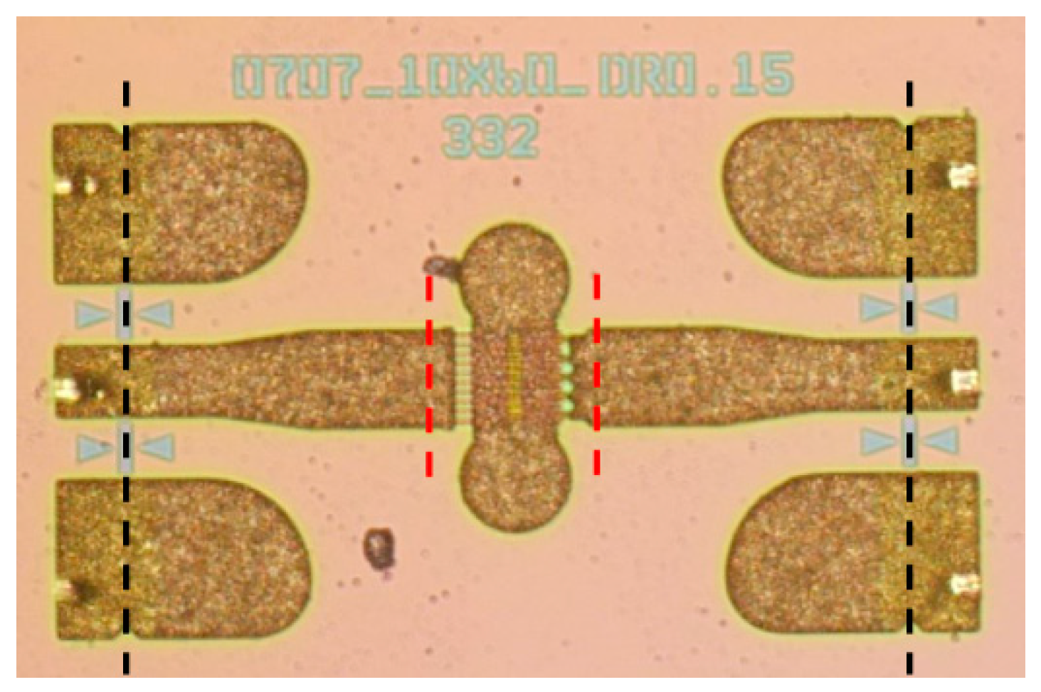
The DUTs have gate lengths of 0.15 μm and scaled gate widths of 2 × 50 μm, 4 × 50 μm, 6 × 50 μm, and 10 × 60 μm. The gate-to-gate pitch is equal to 7 μm for all the devices. The picture of the 10 × 60 μm gate width device has been chosen as a sample and reported in
Figure 1.
In order to compare the experimental results, the same measurement bias point has been used in both laboratories, i.e. drain-source voltage VDS = 2 V and drain-source current density JDS = 200 mA/mm.
A consistent bias point in terms of VDS and current density JDS is a requirement for the tuner-free approach and allows for the comparison of the results obtained by the two approaches. The devices have been characterized by performing the measurements within the 3.5–26 GHz frequency range. The performed measurements consist of:
The measurement campaign has been performed by employing two different calibration kits. At the NRL laboratory, on-wafer standards have been employed to execute a TRL calibration. Therefore, the reference planes have been set at the red dotted lines of
Figure 1.
At the UniME laboratory, off-wafer standards have been used, thus setting the reference planes at the black dotted lines of
Figure 1. The differences resulting in the measurements have been taken into consideration and remarked in
Section 3.
2.1. Tuner-based Measurement Set-up at UniME
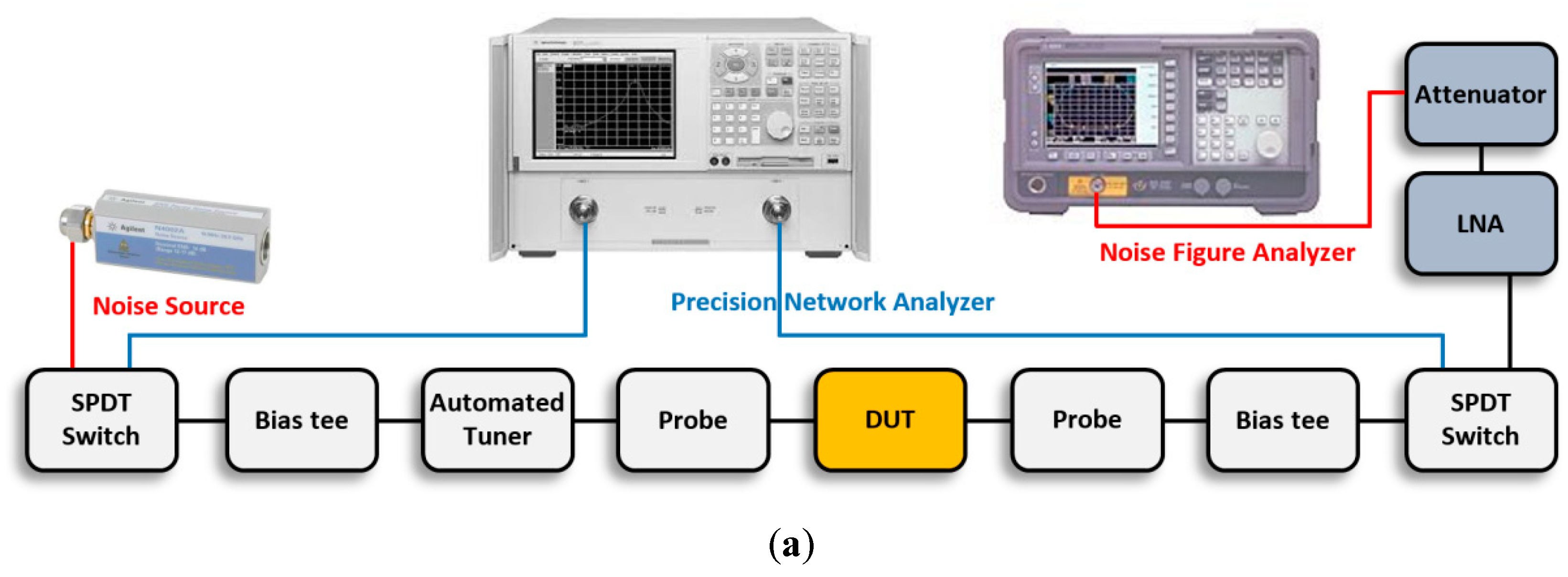
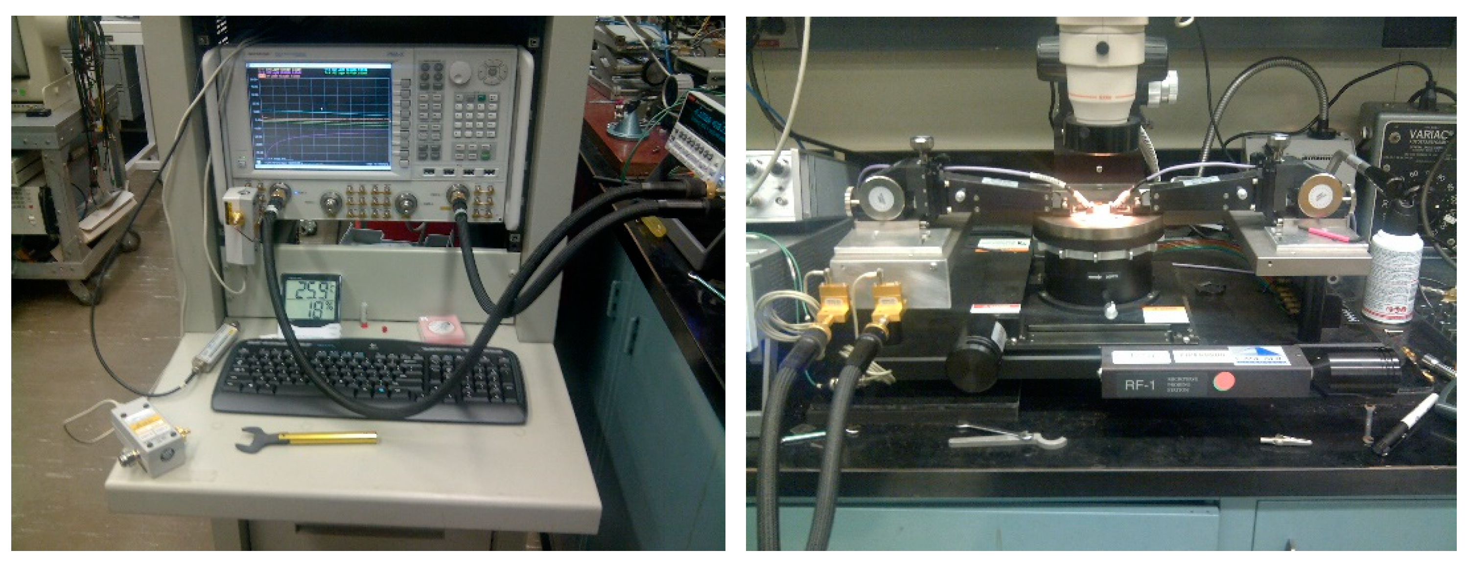
The block diagram and a picture of the measurement system adopted at the UniME laboratory are shown in
Figure 2.
The main instruments of the experimental set-up consist of:
precision network analyzer (Agilent E8364A PNA, 0.045–50 GHz);
noise figure analyzer (Agilent N8975A NFA, 0.01–26.5 GHz);
noise source (Agilent N4002A SNS, 0.01–26.5 GHz),
computer-controlled coaxial tuner (Maury MT-983BU01, 2–26.5 GHz).
Ahead of the noise figure analyzer, a low noise amplifier and an attenuator have been used to set the correct power level handled by the noise figure analyzer. By means of two microwave switches, the input chain can be connected with either port 1 of the network analyzer or the noise source, whereas the output chain can be connected with either port 2 of the network analyzer or the low noise amplifier.
The scattering parameters of the DUTs can be straightforwardly measured by the network analyzer, whereas the determination of the noise parameters requires a complex extraction procedure based on several noise figure measurements [
17,
18].
The extraction procedure employs the definition of the noise factor (
F) as a function of the source reflection coefficient
[
19,
20]:
where
is the reference impedance of 50 Ω,
(
when expressed in dB) is the minimum noise factor that is achieved when
is equal to the complex optimum reflection coefficient
and
is the equivalent noise resistance, that indicates how fast the noise factor degrades when
departs from
. The best condition, i.e., the noise factor equal to the minimum one, can be obtained when
=
.
The extraction of the noise parameters has been performed by exploiting the features of the ATS Maury software. This procedure is based on the Y-factor technique, consisting of measuring for a certain number (at least four) of source impedances made available by the automated tuner.
After selecting the bias point, the scattering parameters have been measured, performing a de-embedding by shifting the reference planes close to the probe tips.
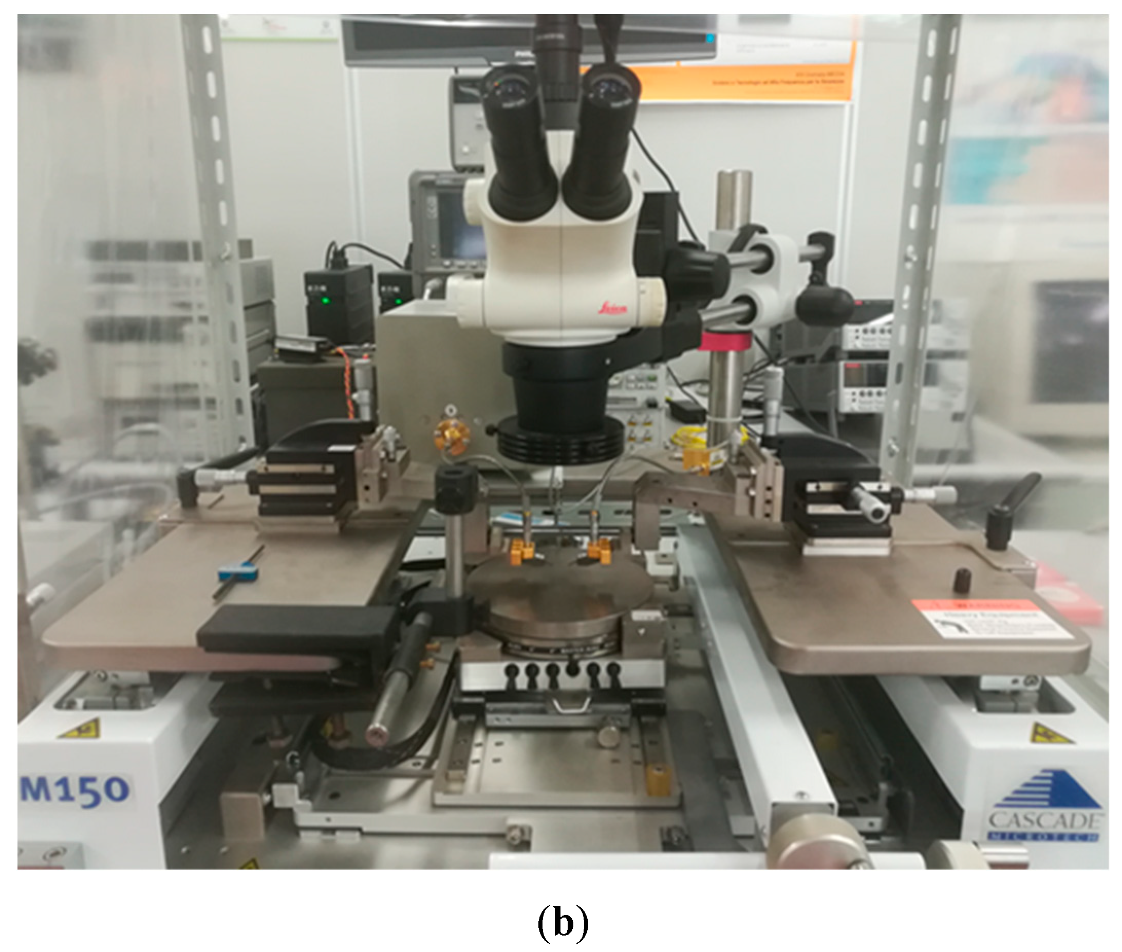
2.2. Tuner-free Measurement Set-up at NRL
The procedure relies on a measurement setup shown in
Figure 3. The setup available at NRL is similar to the one available at UniME and consists of:
a Keysight N5245A PNA-X, operating from 10 MHz to 50.0 GHz;
a fully corrected noise figure H29 Keysight PNA-X personality;
a Keysight N4694 ECal off-wafer electronic calibration setup up to 67.0 GHz;
a Keysight 346C noise source operating from 10 MHz to 26.5 GHz.
The PNA-X noise figure personality operates on the listed PNA-X from 10 MHz to 26.5 GHz because of the use of noise receiver that optimize measurement noise performance. Additional available equipment based on a similar PNA-X model without the noise personality can make noise figure measurements up to 67.0 GHz with the standard receivers (option 028).
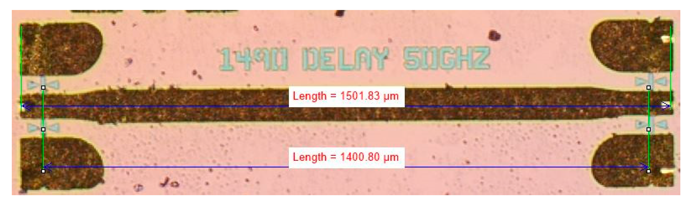
Further, available on-wafer TRL calibration standards have been employed. A sample of delay line used for the on-wafer characterization is shown in
Figure 4. The standard TRL calibration procedure allows the reference planes to be pushed forward from the probe tips to the device gate and drain nodes as depicted in
Figure 1.
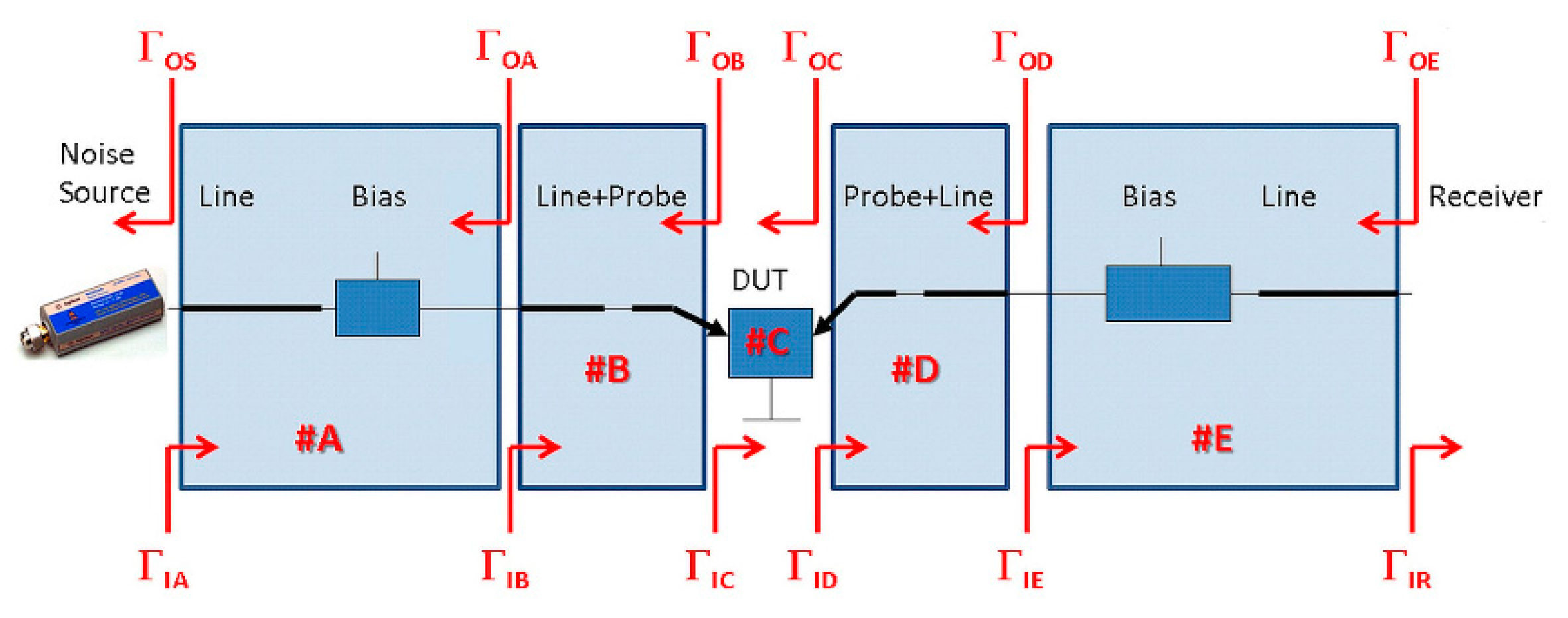
Careful characterization of the measurement setup allows the determination of the small signal parameters for each block in the notional setup shown in
Figure 5.
The measurement of the signal performance of the device is equivalent with the measurement carried out at UniME with the caveat that the reference planes have been shifted from the probe tips to the internal gate and drain planes of the device through additional on-wafer calibration.
On the other hand, the noise performance of the devices under test has been determined without using the additional external tuner. This is possible by shifting the measurement burden to additional calculations once the experimental data is collected. Indeed, in a similar fashion, inspired by the calibration procedures at the basis of the PNA measurements, it is also possible to remove the contributions of the measurement components with simple matrix manipulation of the available data [
21] when considering the noise contribution of each block. In particular, the cascaded blocks A, B, …, E of
Figure 5 will yield an overall noise contribution equal to:
where
is the transmission (ABCD) matrix of the block
and
its correlation matrix in the same representation T. The superscript
is the Hermitian conjugate operator. The correlation matrix
of the device can be obtained with simple matrix subtraction and matrix inversions because:
Hillbrand and Russer [
21] also pointed out that the noise figure can be expressed in terms of the correlation matrix of the device under test. This expression opens up new considerations on the characterization of the noise performance of a linear device [
23], one of which is the evaluation of the device’s noise figure. When considering the transmission T representation, the correlation matrix
can be related to the noise figure by
where
is the source admittance and
is the (hermitian conjugate of the) source vector. The source admittance
is typically corresponding to 50 Ω in a measurement system. However, when shifting the measurement plane away from the source, the admittance
may be a complex number at the frequency of interest due to distributed effects and parasitic components. The exact value for
can easily be determined through the measurement data.
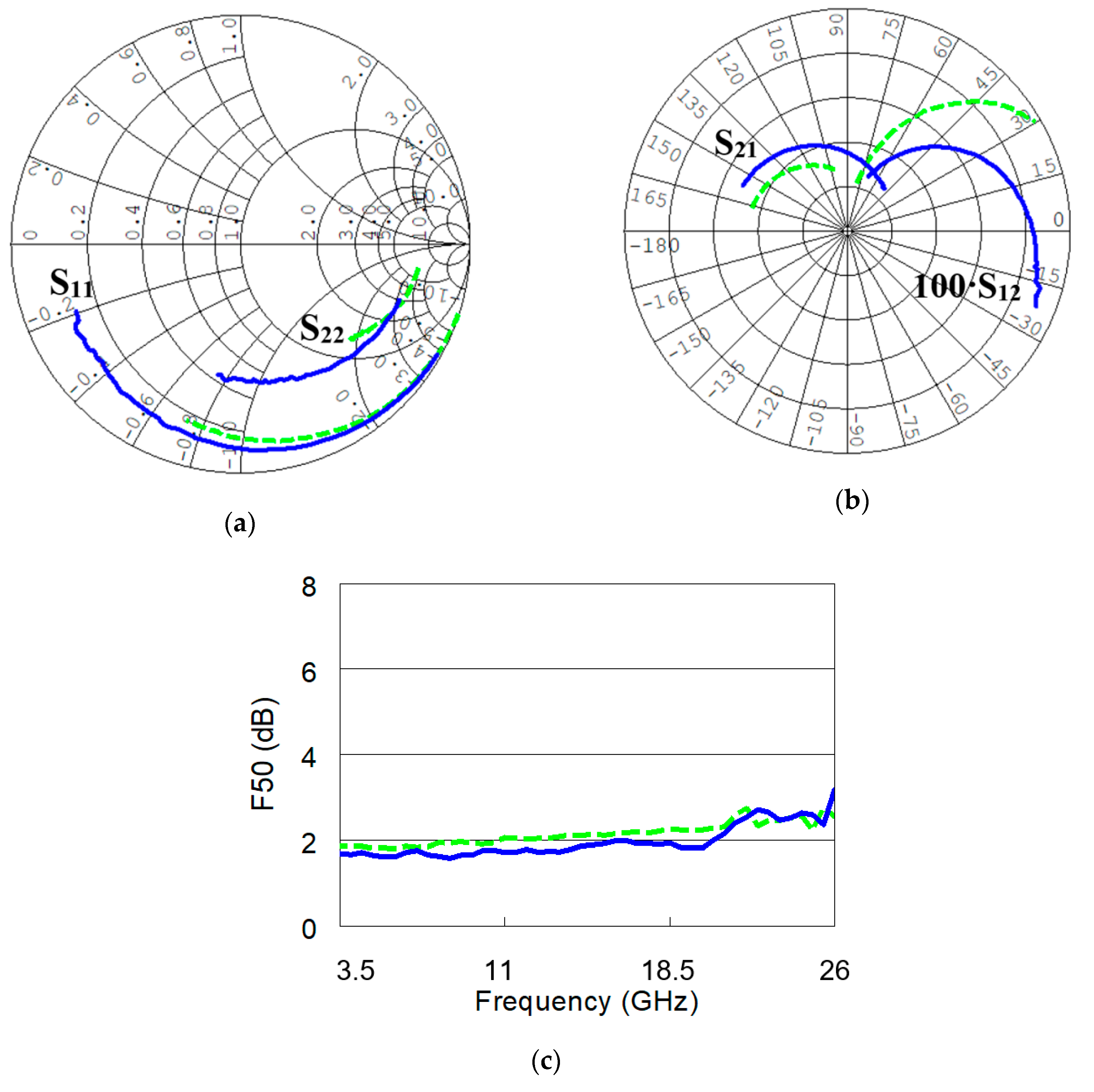
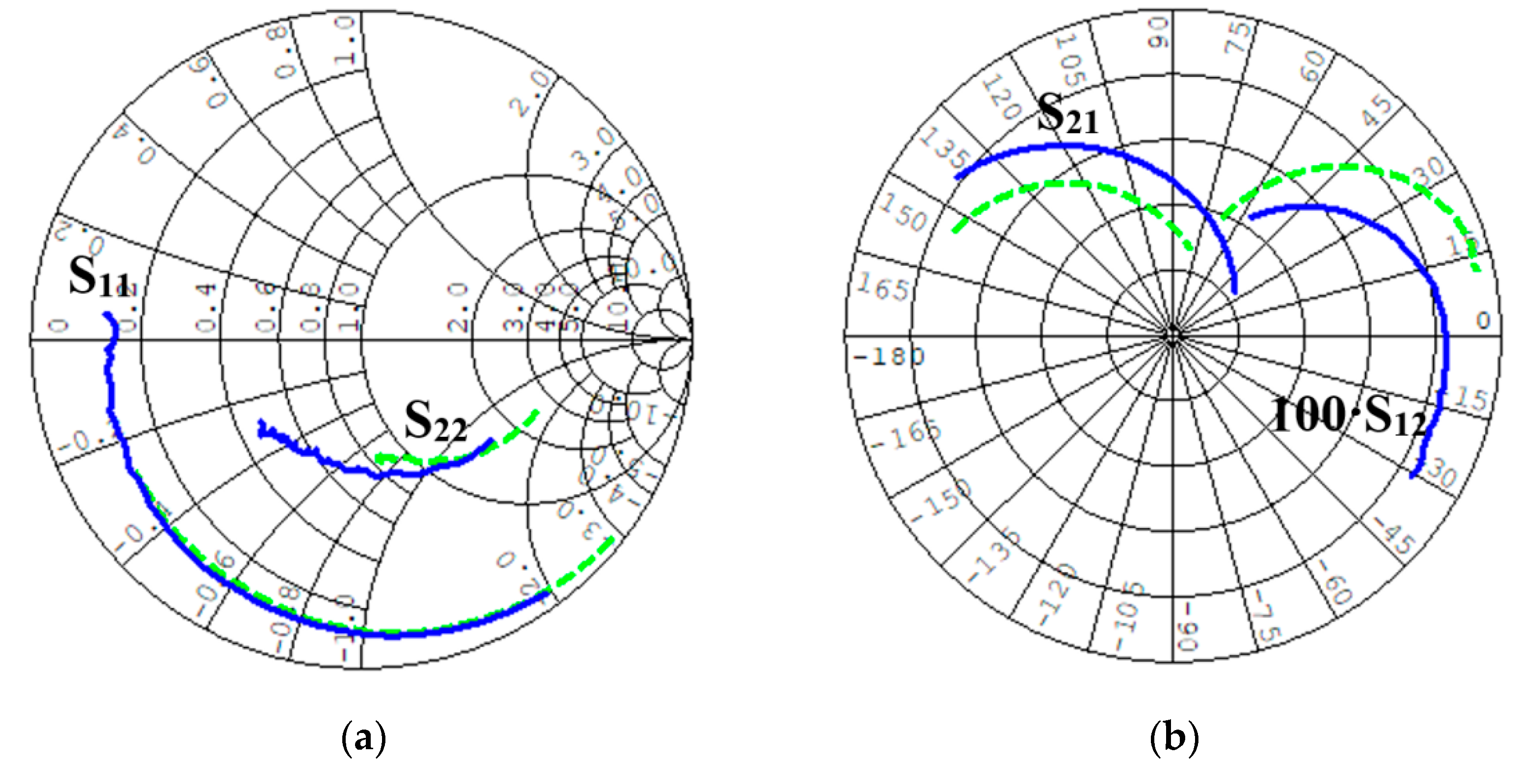
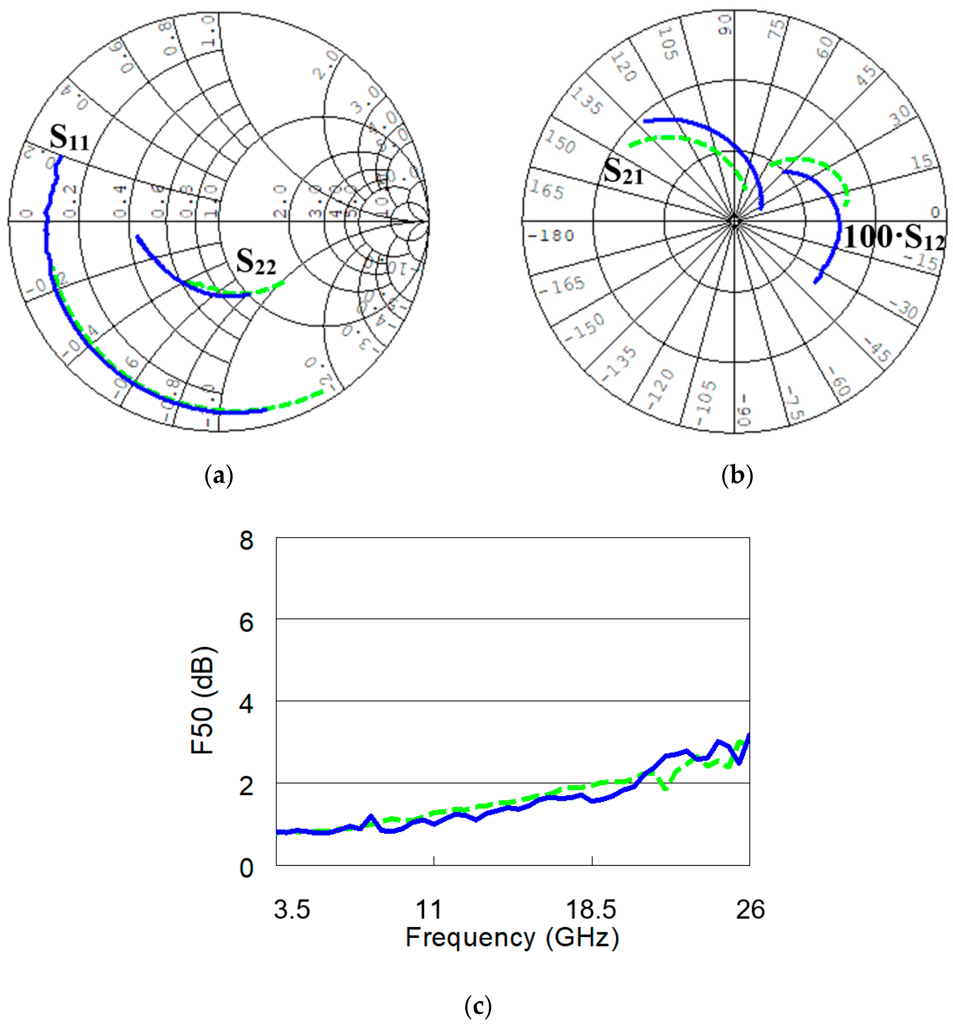
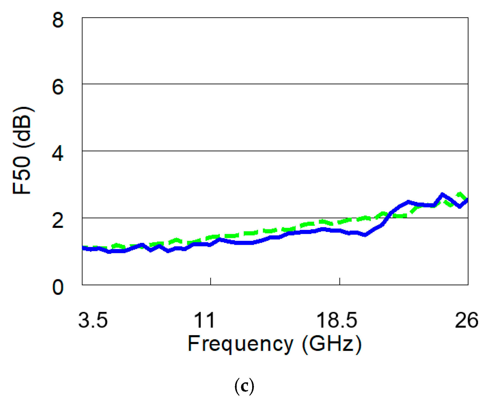
3. Experimental Results and Comparison
As mentioned in
Section 2, the bias point has been fixed to
VDS = 2 V and
JDS = 200 mA/mm, in both laboratories, whereas the measurement have been performed in the frequency range from 3.5 GHz to 26 GHz. From
Figure 6,
Figure 7,
Figure 8 and
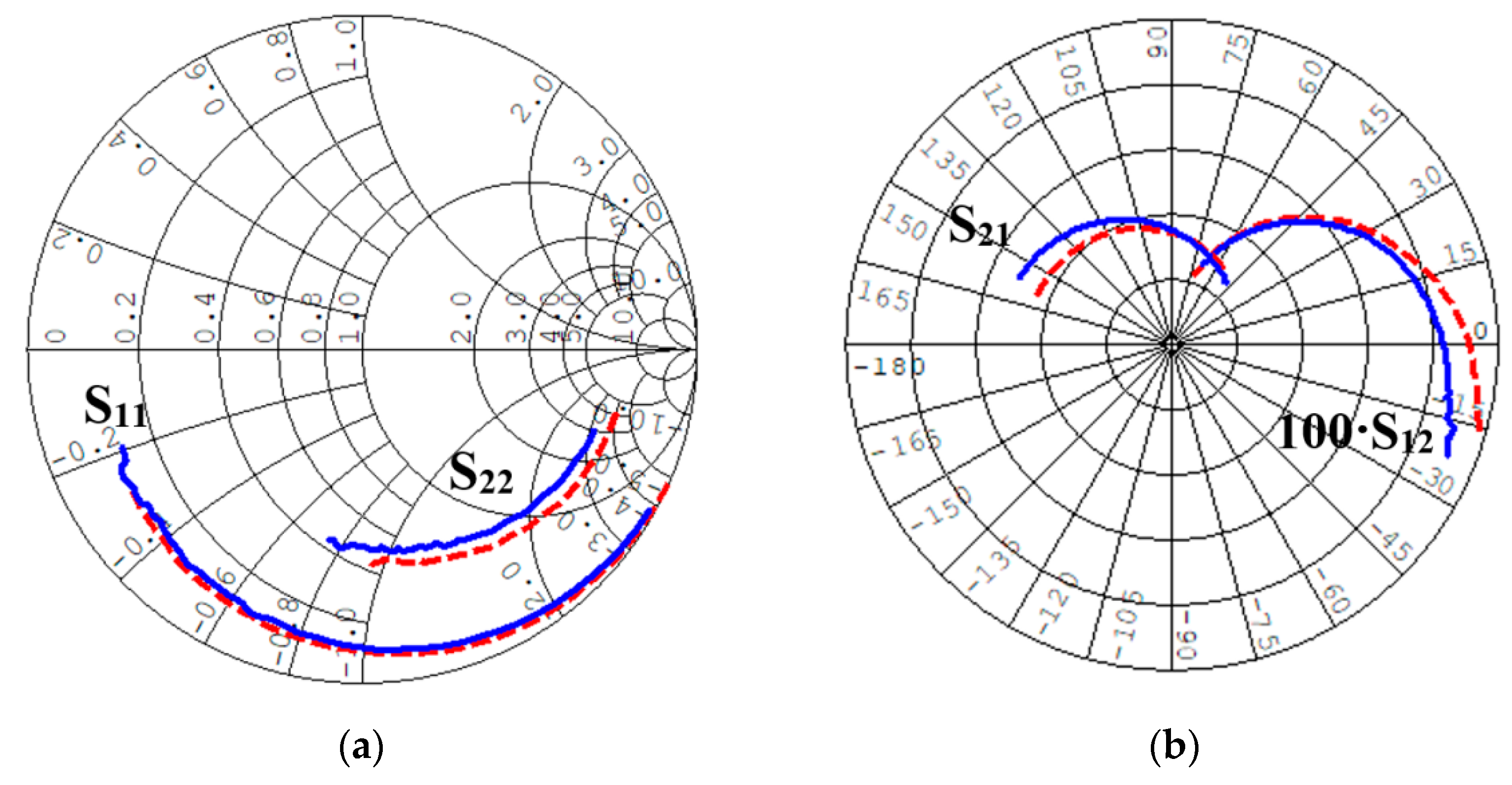
Figure 9 the comparison between the 50 Ω noise figure and the scattering parameters measured at UniME and NRL laboratories is shown. Concerning the scattering parameters, for all the considered devices, the differences between the two sets of measurement are pronounced. Since limited differences could be due to the different measurement location, time and set-up employed for the characterization, these discrepancies in terms of phase rotation and module could be attributed to the shift of the reference planes. Concerning the noise figure, a good correspondence between the two sets of measurements can be noticed. As a matter of fact, the measurements almost overlap. This result is not trivial, considering that the measurements have been performed within two different laboratories with different measurement set-ups, shifted calibration planes, and different procedures employed.
In this regard, the effect of the different reference planes is not so evident. As a matter of fact, the output shift is strongly reduced by the gain of the DUT, whereas the input line, whose losses are negligible, causes only a limited change in the source reflection coefficient value [
17].
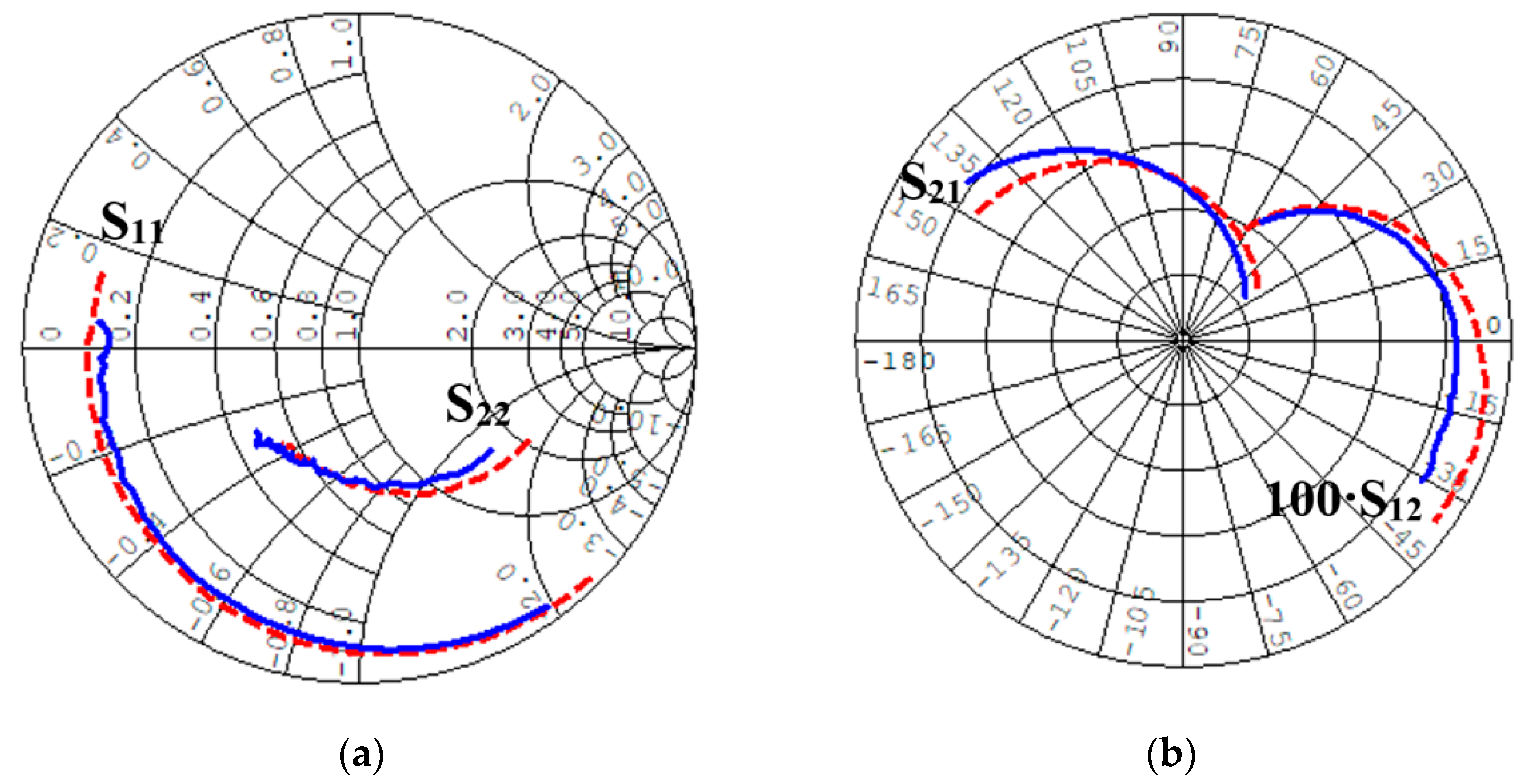
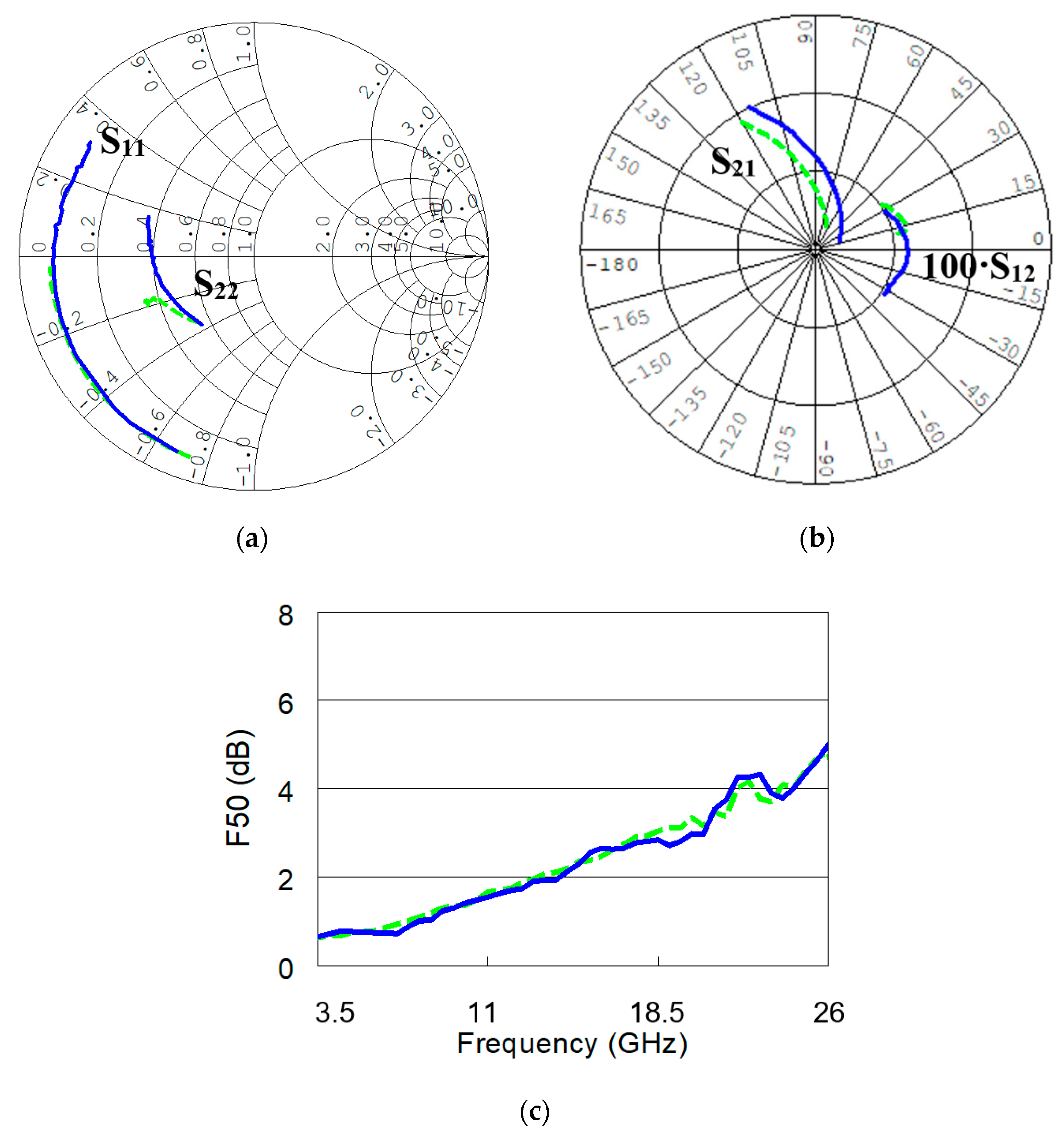
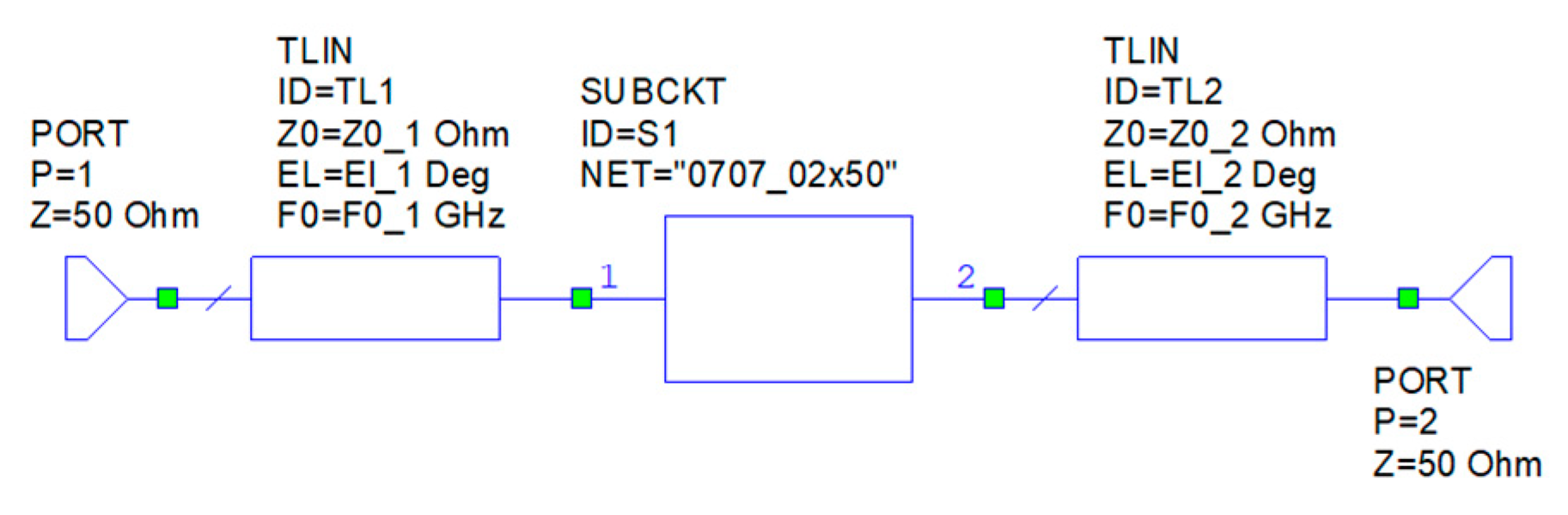
With the twofold purpose of testing the effectiveness of the two test benches and of mitigating the differences between the measurements, the effect of the different reference planes of the UniME setup has been simulated by adding two ideal transmission lines to the input and output ports of the devices measured at the NRL laboratory. This task has been accomplished by employing the National Instruments AWR Design Environment® and, in detail, by considered the aforementioned ideal transmission lines as two additional elements to be attached in series to both the device input and output ports. A schematic representation of a sample device with two ideal transmission lines has been reported in
Figure 10.
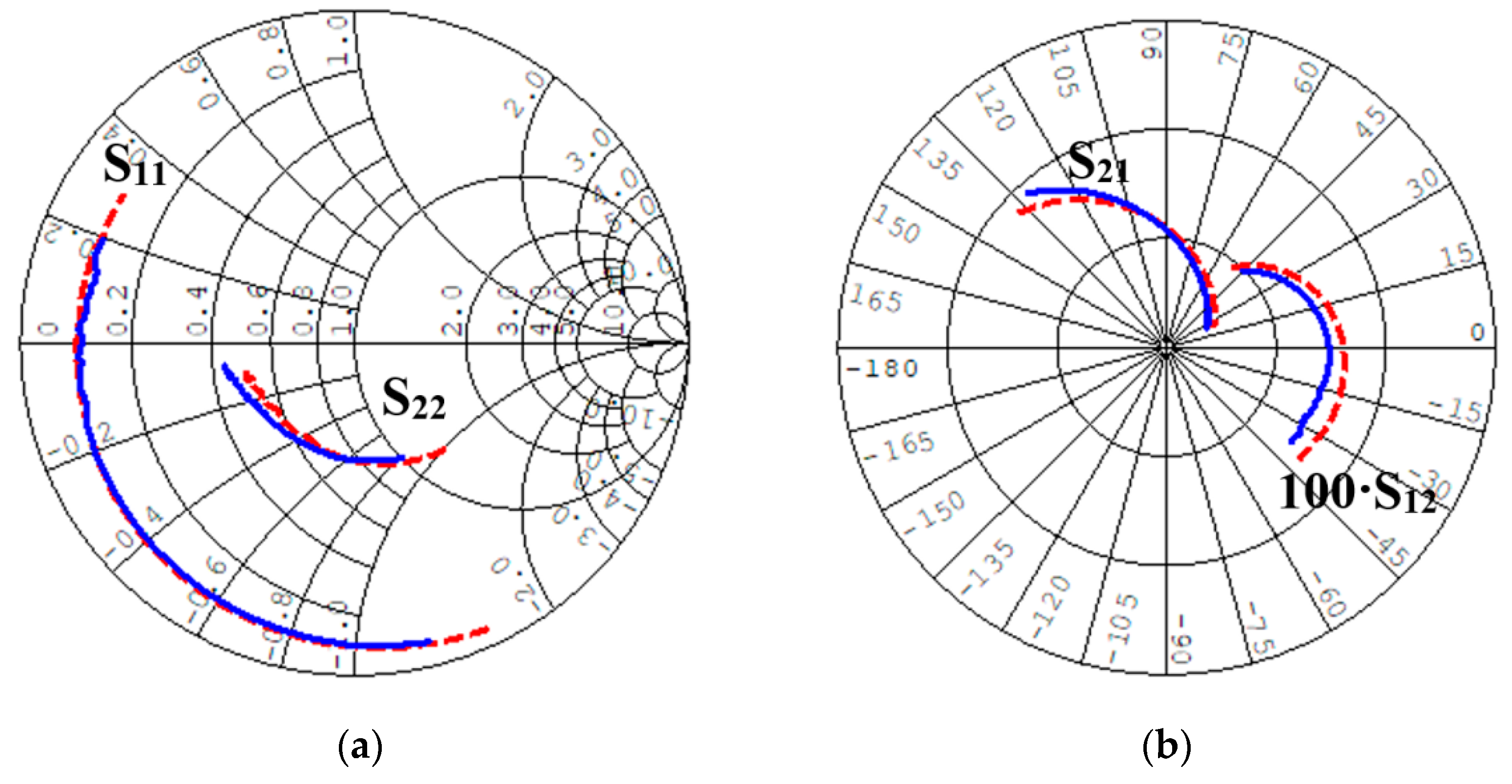
The sub-circuit S1 contains the measured scattering and noise parameters of the device in the touchstone format, whereas the two elements, TL1 and TL2 simulate ideal and lossless transmission lines. The line length is specified as an electrical length (phase lag of mode propagating along the line) at user specified frequency. For both the input and output transmission lines, the values of frequency and characteristic impedance have been fixed equal to the central frequency of 14.75 GHz and 50 Ω. After a manual tuning procedure, the input electrical length has been set equal to 11°, whereas the output one equal to 12°, corresponding to a physical length of 621 μm and 678 μm, respectively. The comparison between the scattering parameters measured at NRL laboratory with the two transmission lines and at the UniME laboratory are shown from
Figure 11,
Figure 12,
Figure 13 and
Figure 14.
The two transmission lines allowed compensating the differences in the reference planes, whose good correspondence is clearly visible from
Figure 11,
Figure 12,
Figure 13 and
Figure 14. The slight differences occurring in the magnitude and phase of the scattering parameters might be due to: a) to the slightly different bias point; b) to the approximation introduced with the ideal transmission lines whose length has been kept fixed for all devices in spite of their different input and output layout topologies.


