Article

A 1.8 V 18.13 MHz Inverter-Based On-Chip RC Oscillator with Flicker Noise Suppression Using Logic Transition Voltage Feedback

School of Electrical Engineering and Computer Science, Gwangju Institute of Science and Technology, Gwangju 61005, Korea
*
Author to whom correspondence should be addressed.
Electronics 2019, 8(11), 1353; https://doi.org/10.3390/electronics8111353
Submission received: 21 October 2019 / Revised: 8 November 2019 / Accepted: 11 November 2019 / Published: 15 November 2019
(This article belongs to the Section Circuit and Signal Processing)

Abstract

:
An inverter-based on-chip resistor capacitor (RC) oscillator with logic transition voltage (LTV) tracking feedback for circuit delay compensation is presented. In order to achieve good frequency stability, the proposed technique considers the entire inverter chain as a comparator block and changes the LTV to control the oscillation frequency. Furthermore, the negative feedback structure also reduces low-frequency offset phase noise. With a 1.8 V supply and at room temperature, the suggested oscillator operates at 18.13 MHz, consuming 245.7 μ W. Compared to the free-running case, the proposed technique reduces phase noise by 7.7 dB and 5.45 dB at 100 Hz and 1 kHz, respectively. The measured phase noise values are −60.09 dBc/Hz at 1 kHz with a figure of merit (FOM) of 151.35 dB/Hz, and −106.27 dBc/Hz at 100 KHz with an FOM of 157.53 dBc/Hz. The proposed oscillator occupies 0.056 mm2 in a standard 0.18 μ m CMOS process.

1. Introduction

As smart devices become more popular and the market demand for wearable devices grows, the need for low-power, on-chip resistor capacitor (RC) oscillators in a standard CMOS process is increasing, to address the cost and board area issues in external crystal oscillators. Owing to their strengths compared with ring oscillators (better frequency stability, control linearity, and wide tuning range), fully integrated relaxation oscillators are widely used as on-chip reference clocks, or as sensor front-end interfaces [1,2]. However, since the figure of merit (FOM) of a relaxation oscillator still cannot reach its theoretical limit [3], several studies are currently ongoing to overcome these circuit issues.
Voltage-to-delay feedback and a switch-capacitor, swing-boosting (SCSB) circuit have been proposed to help improve frequency stability and phase noise characteristics [1], but an SCSB requires a large chip area due to its passive components. In order to reduce comparator noise effects, [2] suggests a differential swing-boosting method with a 162.1 dBc/Hz FOM. However, this scheme requires a high-speed comparator for output frequency stabilization [4]. Filtering the jitter noise in [3] yields a good FOM, while using a low-noise, milliwatt-level, power-hungry block. A feedback structure for frequency stabilization is also introduced in [5,6], but the power consumption in its analog feedback blocks limits its FOM. A low-frequency, inverter-chain-based RC oscillator scheme is presented in [7], achieving a high-voltage swing at its oscillating node. However, as this single-ended approach is vulnerable to circuit delay fluctuations, a regulated supply from a proportional-to-absolution-temperature (PTAT) reference is required, and this leads to a low operating frequency.
In this article, an inverter-based RC oscillator with a logic transition voltage (LTV) tracking feedback method is proposed. The LTV of an inverter is defined where the input and output voltages are the same. While maintaining a boosted voltage slope on the timing capacitor [7] for low-noise operation [2], we replace the local regulated supply scheme with an LTV tracking structure, utilizing a voltage averaging feedback (VAF) concept [5] to obtain a high-frequency oscillator (>1 MHz). The structure of the first-stage inverter is modified so that the feedback loop can control the LTV of this inverter. As a result, the effect of circuit delay on the oscillation frequency is reduced. The suggested structure is not only insensitive to circuit variations, but also suppresses low frequency offset phase noise and flicker noise, due to its negative feedback configuration.
This article consists of six sections. Section 2 demonstrates a conventional RC oscillator and the voltage-averaging feedback concept. In Section 3, the circuit level implementation of the proposed oscillator is described, followed by simulation and measurement results illustrated in Section 4. Finally, we present our conclusions in Section 5.

2. RC Oscillator Architecture

2.1. Conventional RC Oscillator Structure

Figure 1 shows a generally known, conventional RC relaxation oscillator and its timing diagram [8]. For a logical high Φ 1 (and a low Φ 2), the timing capacitor C1 is charged by the constant current source IB, while C2 is grounded. When the voltage across C1 (V1 in Figure 1) reaches the threshold level V R E F , the output of the comparator toggles, causing C1 to discharge and C2 to charge. Conversely, when the voltage on C2 crosses V R E F , C1 charges and C2 discharges. This cycle repeats to create the oscillating function. As shown in the timing diagram in Figure 1, the oscillator output period consists of T O S C , as determined by the timing capacitors, plus the circuit delay. As this delay is sensitive to supply and temperature variation, several methods have been introduced [1,5,8] to stabilize the oscillation frequency. In addition, in order to achieve low noise, [2] introduced a method of increasing the charging/discharging slope of the timing capacitor voltages using a swing booster circuit.
Figure 2 shows the inverter-based RC oscillator scheme introduced in [7]. Biased by the PTAT reference current, a voltage regulator produces a local supply voltage (Local Supply in Figure 2). The circuit delay through the inverter chains causes the almost constant over supply of voltage and temperature variations, because this regulated supply tracks for both NMOS and PMOS thresholds, leading to a stable oscillation frequency. An increased voltage swing across its timing capacitor also helps this structure to achieve low-noise performance. However, a lower local supply voltage limits this scheme to a low oscillating frequency (33 kHz in [7]).

2.2. Voltage Averaging Feedback (VAF) Concept

A voltage-averaging feedback (VAF) method has been proposed in order to achieve good frequency stability in an on-chip CMOS relaxation oscillator [5]. The conceptual waveform is illustrated in Figure 3, where V T H , C O M P and V R E F are the threshold voltage of the comparators and the reference voltage of the VAF integrator, respectively. In its steady state, the active filter in the VAF loop equalizes V R E F and the DC voltage of oscillation, creating the following relationship:
1 T H 0 T H V O S C ( t ) d t = V R E F
0 T H V O S C ( t ) d t = V R E F × T H = Constant
In Equation (2), during T H , the areas of the V O S C and V R E F graphs are the same. If the comparator delay ( δ C O M P s in Figure 3) increases while V T H , C O M P maintains its value, the graph area configured by V O S C increases. Since the area under the graph enclosed by V R E F – the output of a resistive divider – is constant and insensitive to delay variation, the VAF loop lowers V T H , C O M P to satisfy the integration relationship (Figure 3b). In contrast, for a shorter δ C O M P , the feedback structure increases V T H , C O M P to adjust the V O S C curve.
In summary, if the circuit delay is constant, an increase/decrease in V T H , C O M P causes a decrease/increase in the oscillation frequency. Therefore, the VAF technique, by changing the comparator threshold voltage, reduces the effect of circuit delay variation by controlling the frequency.

3. Circuit Level Implementation

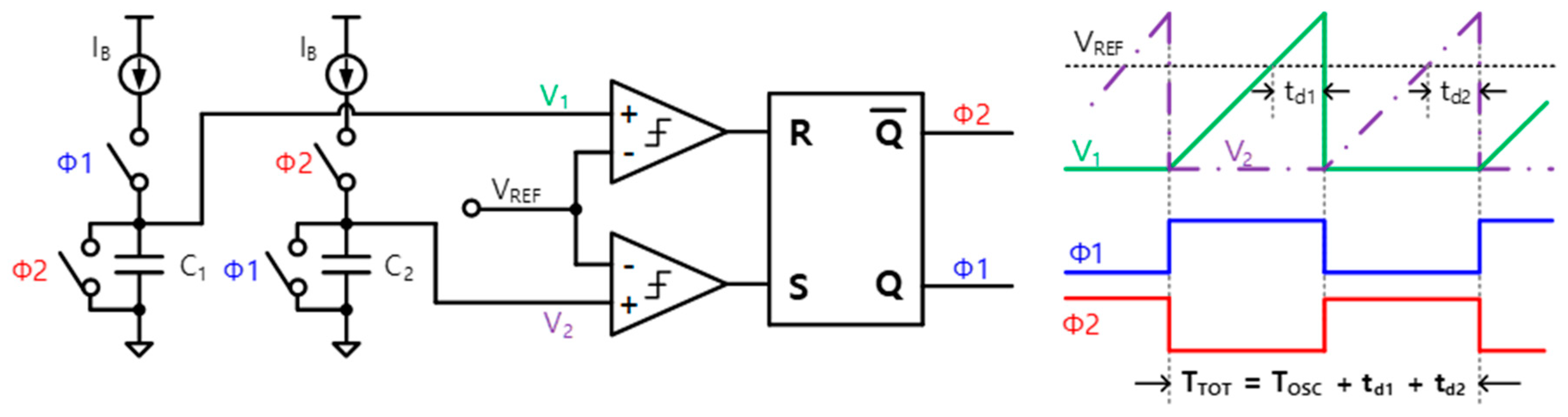
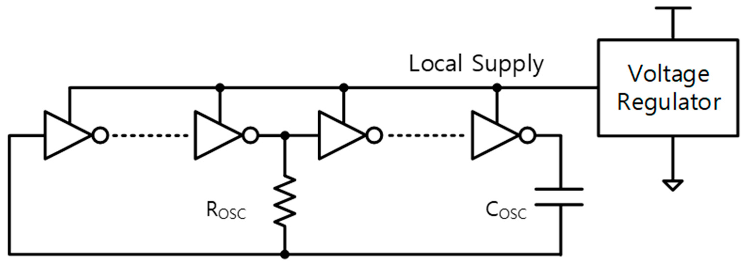
3.1. Oscillating Mechanism of an Inverter-Based RC Oscillator

A simple example of the structure and waveform of an inverter-based RC oscillator is shown in Figure 4. In practice, the gain of the inversion stages (INV1 and INV2 in Figure 4) should be large enough to allow for oscillation, and the proposed oscillator uses multiple inverters to allow for high gain [7]. When the V O S C , V A , and V B nodes are, respectively, high, low, and high, V O S C gradually decreases as R O S C discharges C O S C . When V O S C equals the LTV of INV1, where the input and output voltages are the same, V A and V B change to logical high and low states, respectively. Since the charge on the capacitor should be the same, the voltage change at the V B node lowers the V O S C equally, making V L O W equal to L T V I N V 1   V D D . Next, since the V O S C node voltage decreases while V A stays in the high state, C O S C is charged through R O S C , and the V O S C node voltage increases. Similarly, when the charging V O S C passes the L T V I N V 1 level, the V O S C node voltage rises to V H I G H = L T V I N V 1 +   V D D , due to the logic changes in the following inverters. The timing diagram in Figure 4 shows the charge and discharge cycles of the V O S C node, where td1 and td2 are the circuit delays of the inverter chain.
The discharge curve of V O S C is represented by the following equation:
V O S C , d i s c h a r i n g ( t ) = ( L T V I N V 1 +   V D D ) · e t R O S C C O S C
The charging equation of V O S C is:
V O S C , c h a r i n g ( t ) = ( L T V I N V 1 2 ×   V D D ) · e t R O S C C O S C + V D D .
Therefore, ignoring the circuit delay, the ideal period of the inverter-based RC oscillator is calculated as being:
I d e a l   P e r i o d ( T O S C )        = R O S C C O S C ln ( L T V I N V 1 + V D D L T V I N V 1 ) + R O S C C O S C ln ( L T V I N V 1 2 V D D L T V I N V 1 V D D )        = R O S C C O S C ln [ ( L T V I N V 1 + V D D ) ( L T V I N V 1 2 V D D ) ( L T V I N V 1 ) ( L T V I N V 1 V D D ) ] .
If L T V I N V 1 is equal to half of V D D , the ideal oscillation period T O S C is R O S C C O S C ln ( 9 ) , and the ideal duty cycle is 50% [7].
Taking circuit delay into consideration, the practical period of the oscillator is as follows:
T T O T = T O S C + t d

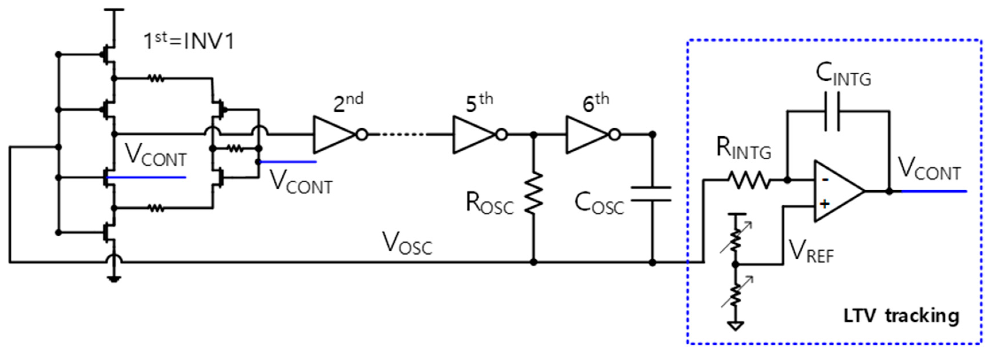
3.2. Architecture of Proposed Oscillator

Figure 5 shows the structure of the proposed inverter-based, on-chip RC oscillator. The inverter chain implemented is as small as possible to ensure low power operation. The second to sixth inverters have a standard structure, but the first-stage inverter (INV1 in Figure 5) has been reconfigured to control its LTV. The V R E F from the resistive divider and V O S C are inputs to the LTV tracking feedback, and its output— V C O N T —controls L T V I N V 1 . Charging and discharging at the V O S C node causes an oscillation due to the inverter logic switching, so the entire inverter chain can be seen to function as a comparator. INV1 is the most sensitive to noise and circuit fluctuations, as the slew rate at its input ( V O S C ) is slower than that of the other nodes. Also, transistor noise in INV1 has a significant effect on circuit delay variation. Thus, because of this sensitivity, INV1 is considered to be the main comparator and its LTV is regarded as the reference voltage for comparison.
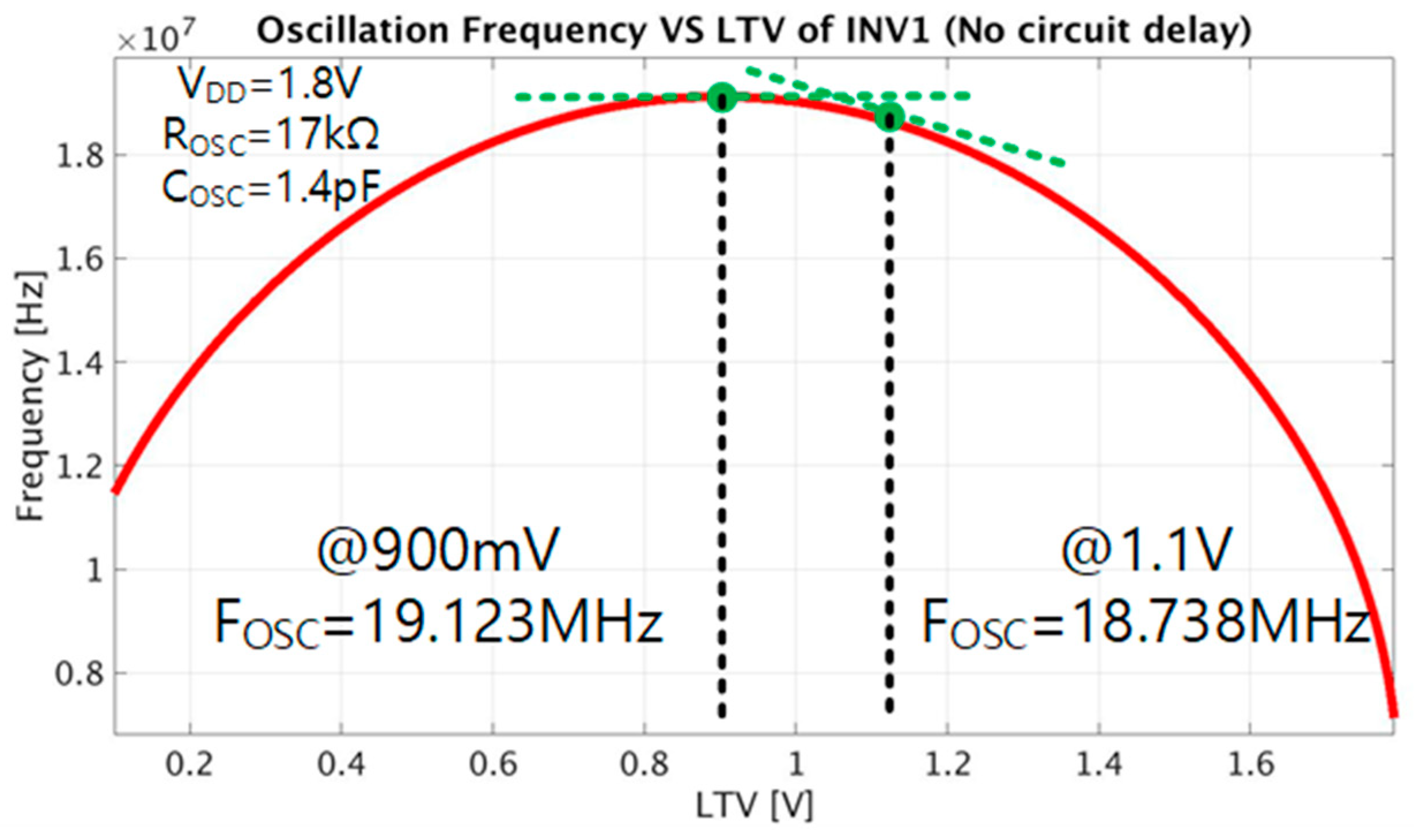
From Equation (5), the operating frequency of the inverter-based RC oscillator without circuit delay is a function of L T V I N V 1 . 
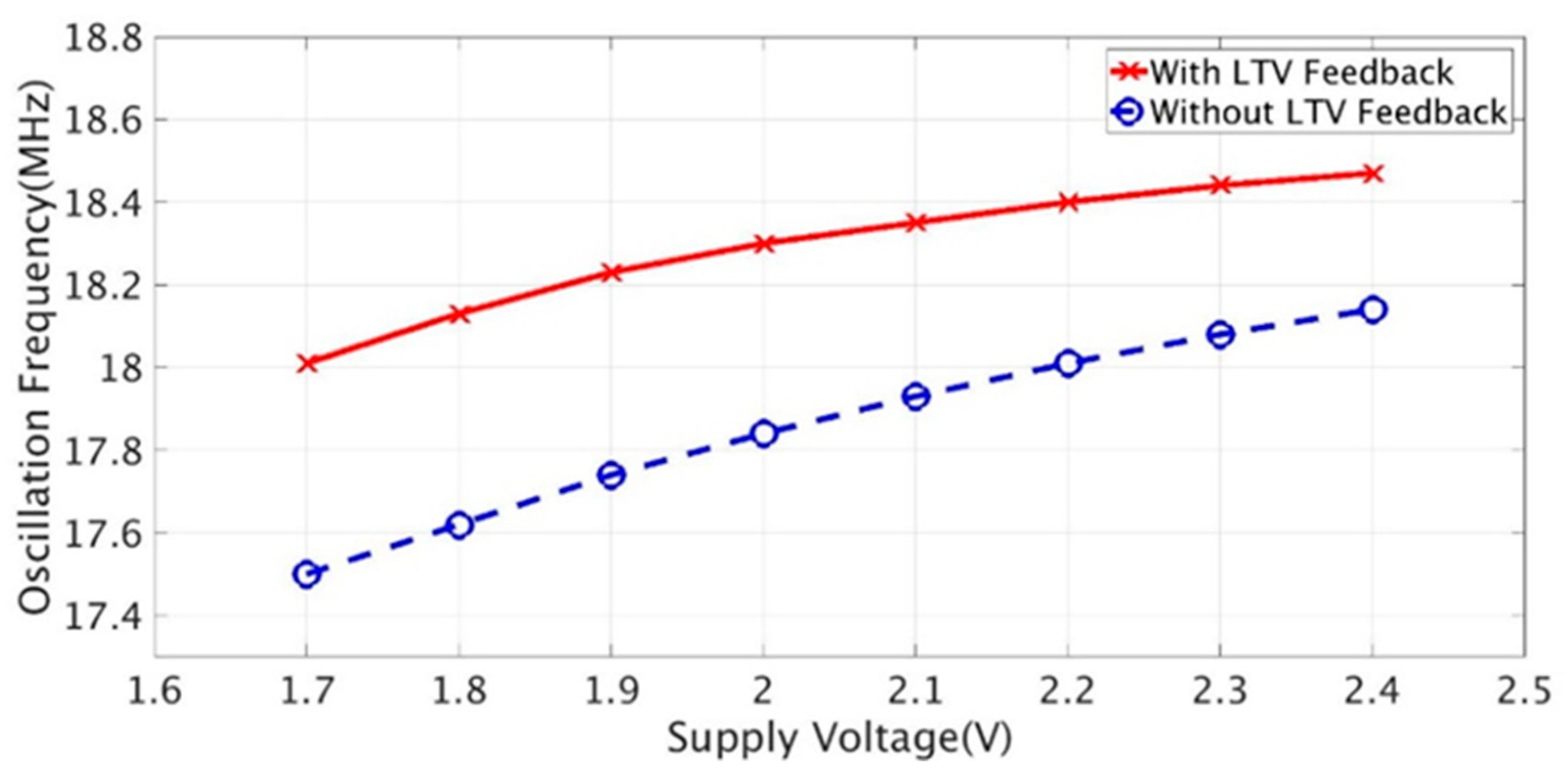
Figure 6 illustrates F O S C (   =   1 / T O S C ) of the oscillator as a function of L T V I N V 1 with V D D = 1.8 V, R O S C = 17 kΩ, and C O S C = 1.4 pF. F O S C is an inverted U-shaped curve with a maximum of 19.123 MHz when INV1 LTV is 900 mV, which is half of V D D .
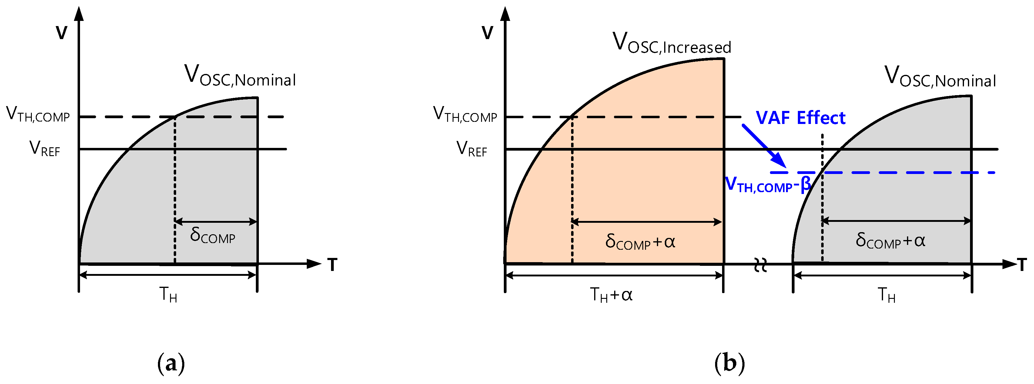
In a practical oscillator, the frequency contains a circuit delay component as expressed in Equation (6), and delay variations degrade the oscillator’s stability. Thus, in order to reduce the influence of these variations, a method is required to detect delay changes and to maintain a constant frequency. As shown in Figure 3, the VAF scheme senses delay variation by comparing graph areas, and the reference voltage of the comparator is changed to maintain a constant frequency.
The suggested LTV tracking technique utilizes the VAF concept for L T V I N V 1 control to reduce the effects of circuit delay variations. The proposed oscillator works by comparing the graph area configured by V O S C and V R E F , to estimate the delay variation. For example, if the circuit delay increases, the V O S C graph area grows while the area under V R E F is unchanged. In addition, as demonstrated in Equation (6), this increased delay causes a decrease in oscillation frequency.
In order to achieve good frequency stability, an operating frequency compensation mechanism that responds to circuit delay variations is required. Figure 6 shows that the oscillation frequency of an inverter-based RC oscillator is determined by the L T V I N V 1 , unless the passive components ( R O S C and C O S C ) change. Thus, the proposed LTV tracking scheme allows for the oscillator to have a constant operating frequency by adjusting the L T V I N V 1 from V C O N T (the feedback loop output).
If the nominal value of L T V I N V 1 is 900 mV (half of the 1.8 V supply), the oscillation frequency variation for the LTV change is close to zero, as indicated by the horizontal tangent line in Figure 6. Furthermore, increasing or decreasing the LTV to around 900 mV only lowers the oscillator frequency relative to the maximum value, so the oscillator cannot cope with longer circuit delay situations. Therefore, because the integrator of the LTV tracking loop makes the DC voltage of V O S C equal to V R E F , the proposed scheme raises the L T V I N V 1 by setting the resistive divider output to 1.1V, in order to control the oscillator frequency against any variations of L T V I N V 1 .
In this approach, the oscillator cannot sustain a 50% duty cycle, but the sensitivity of the operating frequency to L T V I N V 1 is increased (see the increased tangent line slope in Figure 6). When maintaining negative feedback, the increase/decrease of the LTV relative to 1.1 V causes frequency decrease/increase. Considering frequency controllability alone, LTV’s larger than 1.1V can be used, but this will increase power consumption. The proposed structure enables high-frequency operation by connecting the chip supply to the inverter chain, rather than to the regulated supply, and the large voltage swing at the V O S C node reduces the comparator noise of the inverter chain [2].

3.3. The First-Stage Inverter

In a basic inverter structure consisting of one NMOS transistor and one PMOS transistor, it is not easy to change the LTV of the inverters, except for the supply voltage control. Therefore, a structural change of the inverter is required to control L T V I N V 1 . Figure 7a shows the proposed INV1 schematic for LTV control, where V C O N T stands for the output of the feedback loop. Since the input DC voltage from LTV tracking feedback ( V R E F ) is 1.1 V for oscillation frequency control, the V C O N T value is set so that L T V I N V 1 becomes 1.1 V. Transistors PM2 and NM2 are stacked in the output path, and the substrate of NM2 is connected to V C O N T . PM3 and NM3, with V C O N T as inputs, are connected to the main inverter path, forming an auxiliary path through a resistor connected to each source node.
Changing the supply voltage to adjust the inverter’s LTV further lowers the frequency stability of the inverter chain-based RC oscillator. Also, to maintain the supply voltage, a large chip area is required to change the LTV, using the driving current from multiple connected transistors with switches. However, the proposed method controls L T V I N V 1 relative to 1.1 V, by controlling the pull-down strength with V C O N T while using a simple structure. An increased V C O N T reduces the current drive capability of the NMOS pull-down path [9], resulting in a higher L T V I N V 1 . Thus, the oscillation frequency decreases according to Equation (5), as illustrated in Figure 6. In addition, because a decreased V C O N T leads to a lower L T V I N V 1 , an increase/decrease in V C O N T causes a decrease/increase in oscillator frequency.
Figure 7b shows the change in L T V I N V 1 when the control voltage V C O N T varies from 0.9 V to 1.4 V. Since the nominal voltage of L T V I N V 1 is set to 1.1 V, the positive V C O N T turns on the PN diode between the substrate node and the source node of NM2 in Figure 7a. The increase in V C O N T causes the drain-source current of NM2 to be reduced, by increasing its substrate-source diode current while the drain-source current of NM1 is constant. In this situation, L T V I N V 1 increases because the reduced I D S , N M 2 weakens the inverter pull-down strength. Consequently, L T V I N V 1 is controlled by V C O N T which determines the current capability. Furthermore, the auxiliary path consisting of PM3 and NM3 increases the sensitivity of INV1 to the control voltage. This is because the additional structure not only helps the LTV tracking loop settle the output, but also adjusts the amount of INV1 pull-down current.
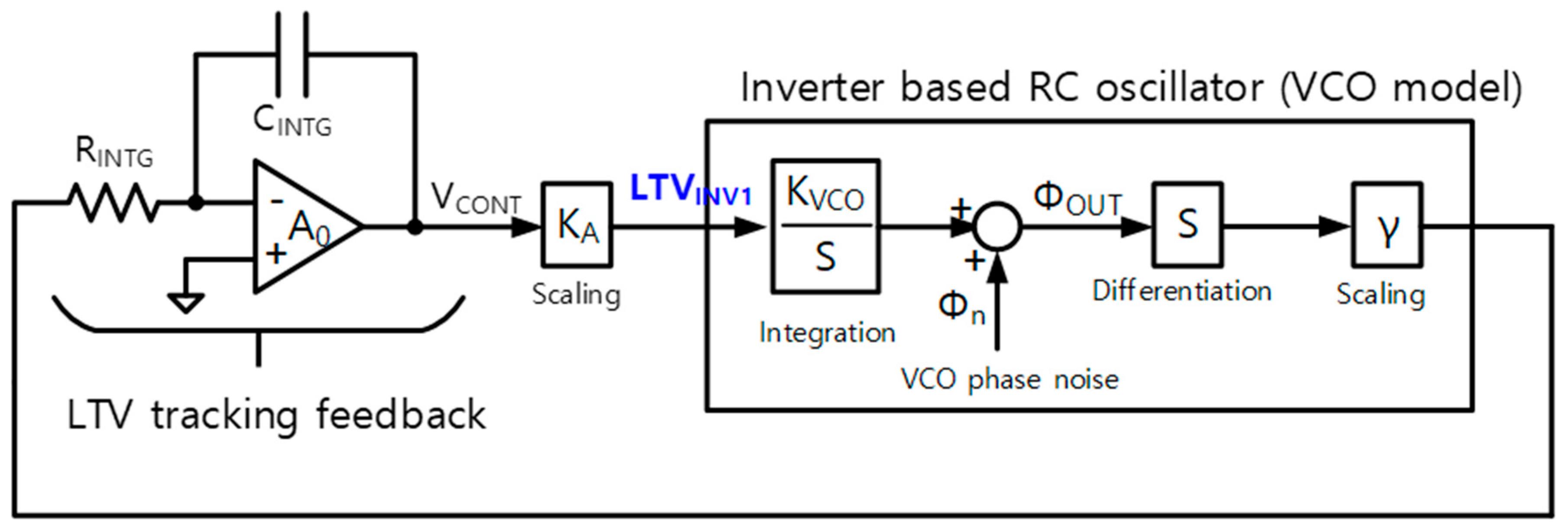
In [
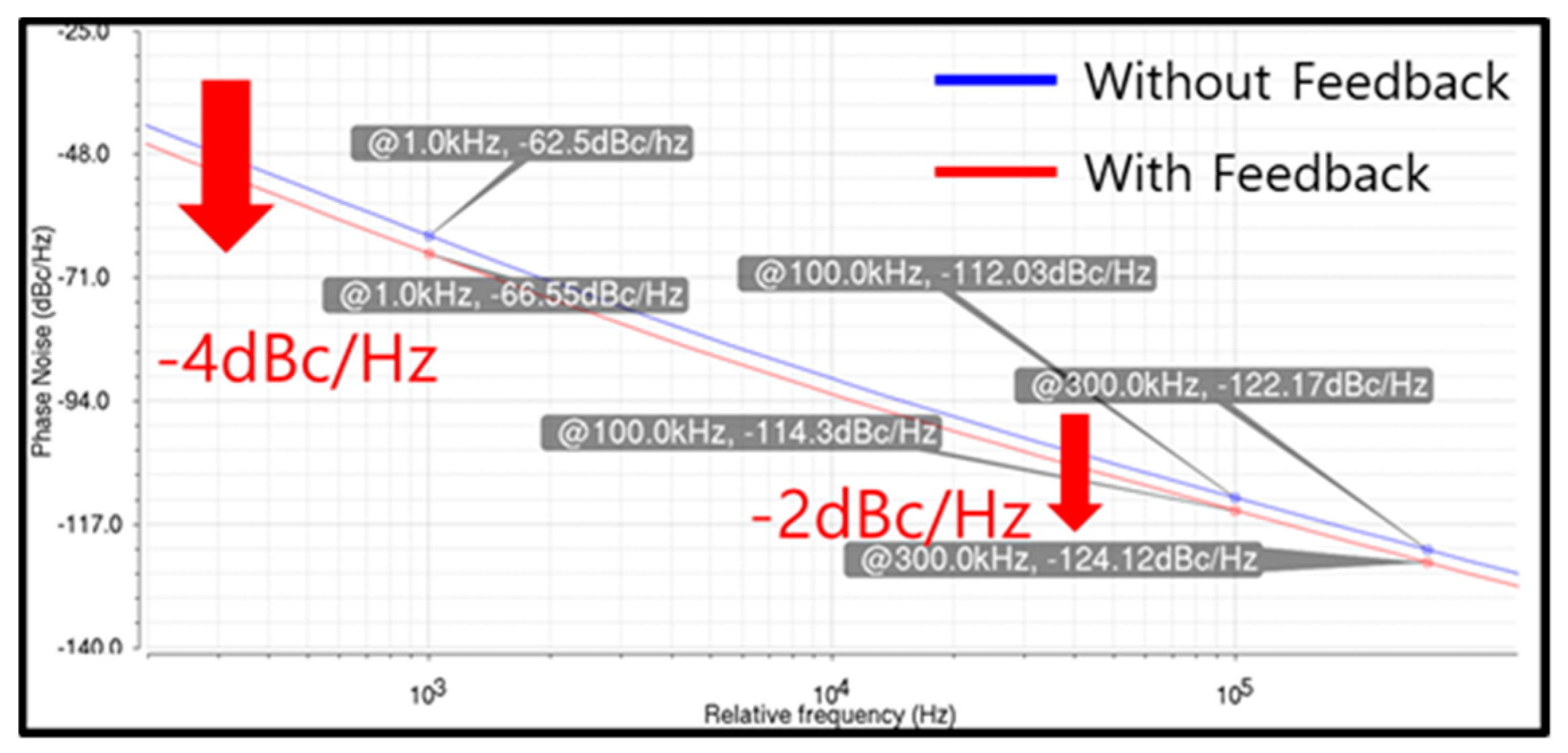
5], the authors introduced an on-chip relaxation oscillator flicker noise suppression method, by modeling the relaxation oscillator as a voltage-controlled oscillator (VCO) and applying the VAF technique. Since the VAF loop creates a high-pass filter, closed-loop transfer function for phase noise, the low-frequency offset phase noise is reduced.
The suggested inverter-based RC oscillator is also a VCO, the frequency of which is controlled by LTVINV1, and we use the VAF concept for the negative feedback structure. The proposed LTV tracking feedback decreases flicker noise in the oscillator, because the noise transfer function in [5] can be applied. Figure 8 shows the noise transfer model, especially for the oscillator phase noise.
The phase noise of the VCO part is formulated as follows:
Φ O U T = s C I N T G R I N T G A 0 + 1 A 0 ( s C I N T G R I N T G + γ K A K V C O ) Φ n
Unlike the phase noise transfer function in [5], Equation (7) requires a voltage scaling factor K A . This is because multiplying the output of the integrator V C O N T by K A produces L T V I N V 1 , which controls the frequency of the oscillator. Equation (7)—with a high-pass, closed-loop transfer function characteristic—has zero and pole at fz and fp, which are described in the following equations:
f z = 1 2 π C I N T G R I N T G A 0
f p = γ K A K V C O 2 π C I N T G R I N T G
Adjusting V C O N T from 1 V to 1.4 V changes the L T V I N V 1 from 1.183 V to 1.02 V, resulting in a K A value of 0.41 (absolute value without polarity). Under this condition, the calculated K V C O is 41.8 × 10⁶ rad/sec · V, and the scaling factor γ is 0.38 V/MHz. Since R I N T G and C I N T G are 1.26 MΩ, and 1.93 pF, respectively, the simulated f p is 652.864 kHz, which is large enough to suppress the low frequency offset phase noise.

4. Simulation and Measurement Results

The proposed LTV tracking, inverter-based RC oscillator was fabricated in a 0.18 μ m standard CMOS process, and Figure 9a shows the layout of the suggested oscillator. Figure 9b illustrates the chip die photo, the active area of which is 310 μ m ×   180 μ m. The passive components that make up the reference voltage divider and the VAF integrating node, especially the resistors, cover a large area. The suggested design, with a nominal 1.8 V power supply, oscillates at 18.13 MHz, consuming 245.7 μ W. Figure 9c shows the simulated power distribution ratio of each block in the proposed oscillator. The highest power consumers are R O S C and the first-stage inverter due to the charge/discharge operation and LTV control
In the INV1 schematic of Figure 8a, the input V C O N T of PM3 and NM3 is disconnected, and the substrate of NM2 is tied to ground in order to implement a feedback-free structure. Figure 10 illustrates the simulated phase noise characteristics. The technique proposed in the simulation reduces oscillator phase noise by 4 dBc/Hz and 2 dBc/Hz at low- and high-frequency offsets, respectively. Figure 11 shows the measured phase noise characteristics when there is (a) no feedback, and (b) the suggested method is applied. As a result of the negative feedback that constitutes the LTV tracking loop, the proposed scheme reduces phase noise at low-frequency offsets. The phase noise at both the 100 Hz and the 1 kHz frequency offsets is decreased by 7.7 dBc/Hz (from –44.72 dBc/Hz to 52.42 dBc/Hz) and 5.45 dBc/Hz (from –54.64 dBc/Hz to –60.09 dBc/Hz), respectively. In the feedback-free structure, circuit noise produces some unwanted tones near 100 kHz, degrading the phase noise characteristics, while the proposed LTV tracking technique filters these tones out but still produces the 400 kHz tones. Compared with the simulation, the overall phase noise level is increased in the measurement. However, the amount of noise suppression remains similar.
The figure of merit (FOM), which measures the performance of an oscillator, can be expressed by the following two equations. L ( Δ f ) , f O S C , and P D I S S represent phase noise at offset frequency, oscillation frequency, and power consumption, respectively.
F O M 1 = | L ( Δ f ) + 20 l o g ( Δ f f O S C ) + 10 l o g ( P D I S S 1 m W ) |
F O M 2 = 10 log ( f O S C P D I S S )
Under the measurement conditions, the proposed oscillator has F O M 1 values of 151.35 and 157.53 at 1 kHz and 100 kHz frequency offsets, respectively, and shows an F O M 2 value of 108.7.
The oscillation frequency, with respect to supply voltage, is illustrated in Figure 12. The solid line depicts the frequency variation of the proposed approach, and the dotted line shows the results without feedback. For a range of 1.7 V to 2.4 V, the proposed oscillator’s frequency variation is calculated as a maximum of 0.365(%/0.1 V), while without feedback, the effect of the supply voltage on the oscillation frequency is 0.522(%/0.1 V).
Table 1 tabulates the performance of the proposed LTV tracking oscillator and other state-of-the-art designs. The oscillators of [5] and [8] display good frequency stability against supply variation, but their respective F O M 1 values are significantly low, due to the degradation of their phase noise characteristics at the offset frequencies. In [2], the highest F O M 1 value was demonstrated, but in comparison, our approach reduces frequency inaccuracy with supply variations. Although our proposal requires a larger chip area for passive components, the method displays FOMs comparable to other methods, due to suppressed phase noise and good frequency stability.

5. Discussion and Conclusions

This article suggests a method of suppressing flicker noise in an inverter-based, on-chip RC oscillator. By changing L T V I N V 1 with an adjusted pull-down strength in the first-stage inverter, the proposed LTV tracking feedback not only compensates for circuit delay variations, but also reduces low-frequency offset phase noise. The proposed oscillator operates at 18.13 MHz, consuming 245.7   μ W from a 1.8 V power supply. The worst-case frequency variation with supply variation is 0.365%/0.1 V. The suggested technique reduces oscillator phase noise by 7.7 dBc/Hz and 5.45 dBc/Hz for 100 Hz and 1 kHz frequency offsets, respectively. Furthermore, the proposed oscillator shows FOM values comparable with those of the latest technologies.

Author Contributions

Conceptualization, J.K.; Methodology, J.K.; Validation, J.K.; Formal analysis, J.K.; Investigation, J.K.; Data curation, J.K.; Writing—original draft preparation, J.K.; Writing—review and editing, J.K.; Visualization, J.K.; Supervision, M.L.; Project administration, M.L.; Funding acquisition, M.L.

Funding

This work was supported by the National Research Foundation of Korea (NRF) grant funded by the Korea government (MSIT) (No. NRF-2019R1A2B5B01069415).

Acknowledgments

The chip fabrication and EDA tool were supported by the IC Design Education Center (IDEC), Korea.

Conflicts of Interest

The authors declare no conflict of interest.

References

  1. Wei, Z.; Wang, L.G.; Yuan, G. A 1.6MHz Swing-Boosted Relaxation Oscillator with ±0.15%/V 23.4ppm/°C Frequency Inaccuracy using Voltage-to-Delay Feedback. In Proceedings of the 2019 IEEE International Symposium on Circuits and Systems (ISCAS), Sapporo, Japan, 26–29 May 2019. [Google Scholar]
  2. Junghyup, L.; Arup, G.; Minkyu, J. A 1.4V 10.5MHz Swing-Boosted Differential Relaxation Oscillator with 162.1dBc/Hz FOM and 9.86psrms Period Jitter in 0.18μm CMOS. In Proceedings of the 2016 IEEE International Solid-State Circuits Conference (ISSCC), San Francisco, CA, USA, 31 January–4 February 2016. [Google Scholar]
  3. Paul, F.J.G.; Ed, V.T.; Eric, A.M.K.; Gerard, J.M.W.; Bram, N. A 90μW 12MHz Relaxation Oscillator with a -162dB FOM. In Proceedings of the 2008 IEEE International Solid-State Circuits Conference (ISSCC), San Francisco, CA, USA, 3–7 February 2008. [Google Scholar]
  4. Jahyun, K.; Kyoung-Sik, M.; Byungsub, K.; Hong-June, P.; Jae-Yoon, S. A Quadrature Relaxation Oscillator with a Process-Induced Frequency-Error Compensation Loop. In Proceedings of the 2017 IEEE International Solid-State Circuits Conference (ISSCC), San Francisco, CA, USA, 5–9 February 2017. [Google Scholar]
  5. Yusuke, T.; Shiro, S.; Akinori, M.; Shiro, D. An On-Chip CMOS Relaxation Oscillator with Voltage Averaging Feedback. JSSC 2010, 45, 1150–1158. [Google Scholar]
  6. Ying, C.; Paul, L.; Wouter, D.C.; Michiel, S. A 63,000 Q-Factor Relaxation Oscillator with Switched-Capacitor Integrated Error Feedback. In Proceedings of the 2013 IEEE International Solid-State Circuits Conference Digest of Technical Papers (ISSCC), San Francisco, CA, USA, 17–21 February 2013. [Google Scholar]
  7. Danielle, G.; Per, T.R.; James, M.; Ryan, S. A 190nW 33kHz RC Oscillator with ±0.21% Temperature Stability and 4ppm Long-Term Stability. In Proceedings of the 2014 IEEE International Solid-State Circuits Conference Digest of Technical Papers (ISSCC), San Francisco, CA, USA, 9–13 February 2014. [Google Scholar]
  8. Jiacheng, W.; Wang, L.G.; Xin, L.; Jun, Z. A 12.77-MHz 31 ppm/°C On-Chip RC Relaxation Oscillator with Digital Compensation Technique. TCAS-I 2016, 63, 1816–1824. [Google Scholar]
  9. Razavi, B. Design of Analog CMOS Integrated Circuits, 2nd ed.; McGraw-Hill Education: New York, NY, USA, 2017; pp. 7–38. [Google Scholar]
Figure 1. Conventional RC relaxation oscillator and its waveform.
Electronics 08 01353 g001
Figure 2. Inverter-based RC oscillator with a regulated local supply [7].
Electronics 08 01353 g002
Figure 3. Conceptual waveforms of the on-chip relaxation oscillator with voltage averaging feedback [5]: (a) nominal case; (b) in case of increased comparator delay with threshold voltage correction.
Electronics 08 01353 g003
Figure 4. Inverter-based RC oscillator and its waveform.
Electronics 08 01353 g004
Figure 5. Proposed inverter-based on-chip RC oscillator.
Electronics 08 01353 g005
Figure 6. Oscillation frequency of the proposed inverter-based RC oscillator with respect to the LTV of the first-stage inverter when circuit delay is ignored.
Electronics 08 01353 g006
Figure 7. (a) Schematic of the first-stage inverter (INV1); (b) Simulated L T V I N V 1 with respect to a V C O N T range of 0.9 V to 1.4 V.
Electronics 08 01353 g007
Figure 8. Noise transfer model of the proposed oscillator.
Electronics 08 01353 g008
Figure 9. (a) Layout of the suggested oscillator; (b) chip photomicrograph of the proposed oscillator; (c) simulated power consumption pie chart.
Electronics 08 01353 g009
Figure 10. Simulated phase noise of the proposed oscillator. The blue line and red line represent without the feedback and with the feedback, respectively.
Electronics 08 01353 g010
Figure 11. Measured phase noise of the proposed oscillator: (a) without the feedback mechanism; (b) with the feedback mechanism.
Electronics 08 01353 g011
Figure 12. Measured oscillation frequency for the supply voltage.
Electronics 08 01353 g012
Table 1. Performance Summary.
Reference[1][2][3][5][8]THIS WORK
Process(nm)18018065180180180
ApproachVoltage-to-delay FeedbackSwing boostingSwitched capacitorVoltage averaging feedbackDigital CompensationInverter- based RC and LTV tracking feedback
Area(mm2)0.1170.0150.030.040.0120.056
Frequency (MHz)1.610.512.51412.7718.13
Jitter (ps)N.A.9.86N.A.3078.746.61
Supply (V)11.41.31.80.91.8
Supply Var. (worst) (%/0.1 V)0.05
@1.2–1.52 V
0.44
@1.4–2 V
N.A.0.08
@1.7–1.9 V
0.1
@0.6–1.1 V
0.365
@1.7–2.4 V
Power ( μ W)51.4219.891 1/3600 24556.2245.7
F O M 1
@1kHz
N.A.157.7N.A.N.A.133.3151.35
F O M 1
@100kHz
156162.1162 1/148 2146140.3157.53
F O M 2 104.9106.8111.4 1
95.4 2
114.9113.6108.7
1 Excludes the power of the anti-jitter comparator. 2 Includes the power of the anti-jitter comparator.

