1. Introduction
Real-time biomedical imaging is a crucial component of biomedical systems pursuing both a real-time diagnosis with the timely evaluation of the interested functional or pathophysiological conditions and a real-time treatment with the closed-loop optimization of the intervention [
1,
2]. Although high-resolution computed tomography (CT) and magnetic resonance imaging (MRI) provide the highest penetration depth over 10 cm with decent sub-mm resolution, they can be hardly used in real-time applications unless the resolution is significantly sacrificed, because of the time-consuming scanning and image processing [
3,
4]. Instead, ultrasound echography, X-ray mammography, confocal microscopy, near-infrared fluorescence (NIR), and optical coherence tomography (OCT) have been actively adopted for the real-time biomedical imaging applications for both clinical and research settings [
5,
6,
7]. However, several limitations such as low resolution, small focal area, artifacts from bony structures, and high cost, still hinder the widespread usage of the real-time biomedical imaging.
The millimeter-wave (mm-wave) frequency range, which is defined as a range from 30 to 300 GHz, has recently gained a lot of attention from researchers due to its massive potential to be used for real-time high-resolution biomedical imaging, radar imaging, and spectroscopy [
8,
9,
10,
11]. The mm-wave imaging approach can provide several advantages over the currently-available imaging solutions, such as: (1) low cost with well-established semiconductor process, (2) high-resolution ranging from sub-mm to sub-cm range, (3) low safety risk with non-ionizing radiation, and (4) easy examination process for doctors and patients with integrated handheld devices [
8,
9,
10,
11,
12,
13,
14]. The mm-wave imaging approach has been showing its feasibility in recent years. For example, a complete dielectric profile of breast cancer could be reconstructed [
13] and properties of the early-stage skin cancer tissues could be detected [
14], by the mm-wave imaging technique.
To implement the imaging system at the mm-wave frequency range, the implementation of a signal source with high output power is a big challenge because of the parasitic components that significantly attenuate the output power. Note that the output power matters not just for the penetration depth but for the spatial resolution with a better signal-to-noise ratio. Among several candidates that can implement a high-quality signal source in the mm-wave frequency range, the CMOS technology stands out because of its reliability, low cost, compact size, and advantages of system-on-a-chip integration [
15,
16,
17]. However, CMOS technology has difficulties in implementing signal source at mm-wave frequency range, because of the limited output power with ~300 GHz maximum oscillation frequency (f
max) where unilateral power gain becomes unity [
18,
19,
20].
Recently, several works have been reported to address the challenges in the mm-wave signal source design [
21,
22,
23,
24,
25,
26,
27,
28,
29]. An oscillator in [
27] operates at a center frequency of 190.5 GHz with a maximum output power of −2.1 dBm. However, this oscillator was implemented with an advanced and expensive SiGe compound semiconductor. A signal source, which is presented in [
28] and uses the harmonic frequency to overcome the low f
max of the CMOS technology, generates a low output power of −4.8 dBm at the 2nd harmonic frequency of 239 GHz. However, the generated output power from the harmonic oscillator is low. Another oscillator in [
29] generates an output power of −3.8 dBm at the 2nd harmonic frequency of 163.5 GHz at a typical supply voltage of 1.2 V. However, the maximum output power of 1 dBm at 164.6 GHz was measured at the supply voltage of 2 V, which is much higher than the typical supply voltage guaranteed in a 65 nm CMOS process, which can cause voltage stress and raise reliability problems in active devices. In [
25], another approach, a fundamental frequency cross-coupled oscillator (XCO) with a capacitive-load-reduction-circuit (CLRC) technique, was presented to address the limitations of the CMOS technology. This approach improves the oscillation frequency by suppressing the effect of the load capacitance on the oscillation frequency. Moreover, a differential to single (DTS) transformer is adopted at the output port of the presented topology to enhance the output power.
This paper proposes a novel mm-wave frequency CMOS oscillator with a high output power and a high oscillation frequency by stacking a frequency-selective negative resistance (FSNR) circuit on the top of the XCO with CLRC which is presented in [
25]. The stack structure adds an additional negative resistance which is generated by a FSNR circuit in parallel with a negative resistance of the oscillator core, so a higher output power can be obtained. In addition, the proposed oscillator operates at a higher oscillation frequency since the equivalent inductive reactance of the FSNR circuit combines in parallel with CLRC. Measurement results of the proposed oscillator at 190 GHz show the highest output power among reported oscillators in similar oscillation frequency range, supply voltage, and 65 nm CMOS process.
In
Section 2, the structure and effect of the FSNR circuit on the oscillation frequency and negative resistance of proposed mm-wave oscillator are analyzed. The oscillation frequency and the negative resistance of the conventional XCO, the XCO with CLRC, and the proposed oscillator are compared.
Section 3 presents measurement setups and measurement results of the implemented proposed oscillator. Finally,
Section 4 summarizes the findings in this paper.
2. The Proposed Millimeter-Wave Oscillator
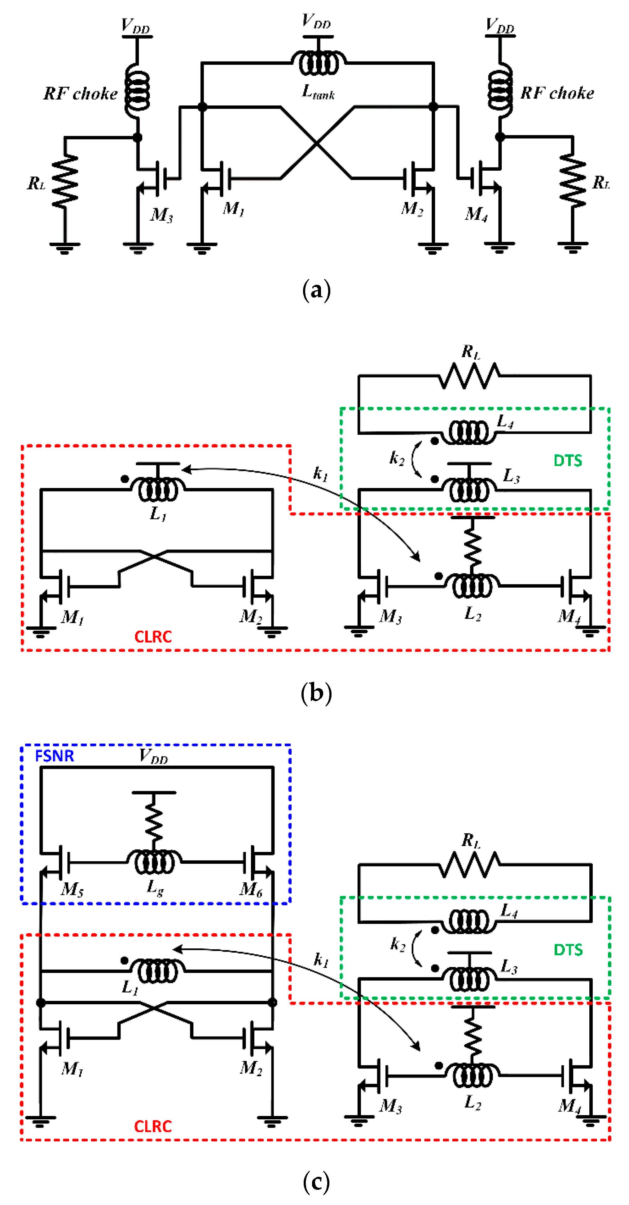
Figure 1 shows the schematic of the conventional XCO, which consists of two NMOS transistors (M
1–M
2), an inductor
Ltank, and two buffer transistors (M
3–M
4). In the conventional XCO, the buffer transistors are directly connected to the main resonant tank, so the parasitic capacitance C
GS at the gate terminals of buffer transistors decrease the fundamental oscillation frequency.
Figure 1b shows the schematic the XCO with CLRC [
25]. In the XCO with CLRC, the CLRC comprises the gates of buffer transistors that are connected to the main resonant tank through a transformer. The transformer in the CLRC couples with the signal from a primary winding
L1 to a secondary winding
L2, by a coupling factor
k1. The function of CLRC is to suppress the effect of the load capacitance on the fundamental oscillation frequency [
25]. The DTS transformer is constructed by
L3 and
L4, at the output port to improve the output power by converting two differential signals into one single-ended signal. As a result, the oscillation frequency and the output power of the XCO with CLRC are higher than that of the conventional XCO.
Figure 1c shows the proposed oscillator structure. The proposed oscillator is formed by stacking an FSNR at the top of the main resonant tank of the XCO and the oscillation signals are coupled through CLRC and the DTS transformer. The FSNR structure is formed by two transistors (M
5–M
6) and an inductor
Lg that is connected at the gate terminals of
M5 and
M6. Resistors are connected to the center taps of
L2 and
Lg to guarantee the differential mode operation by suppressing the common mode operation of the proposed oscillator. These resistors also protect transistors from breakdown by limiting the inrush current flowing from a power supply to the gates of the transistors at the turn-on moment.
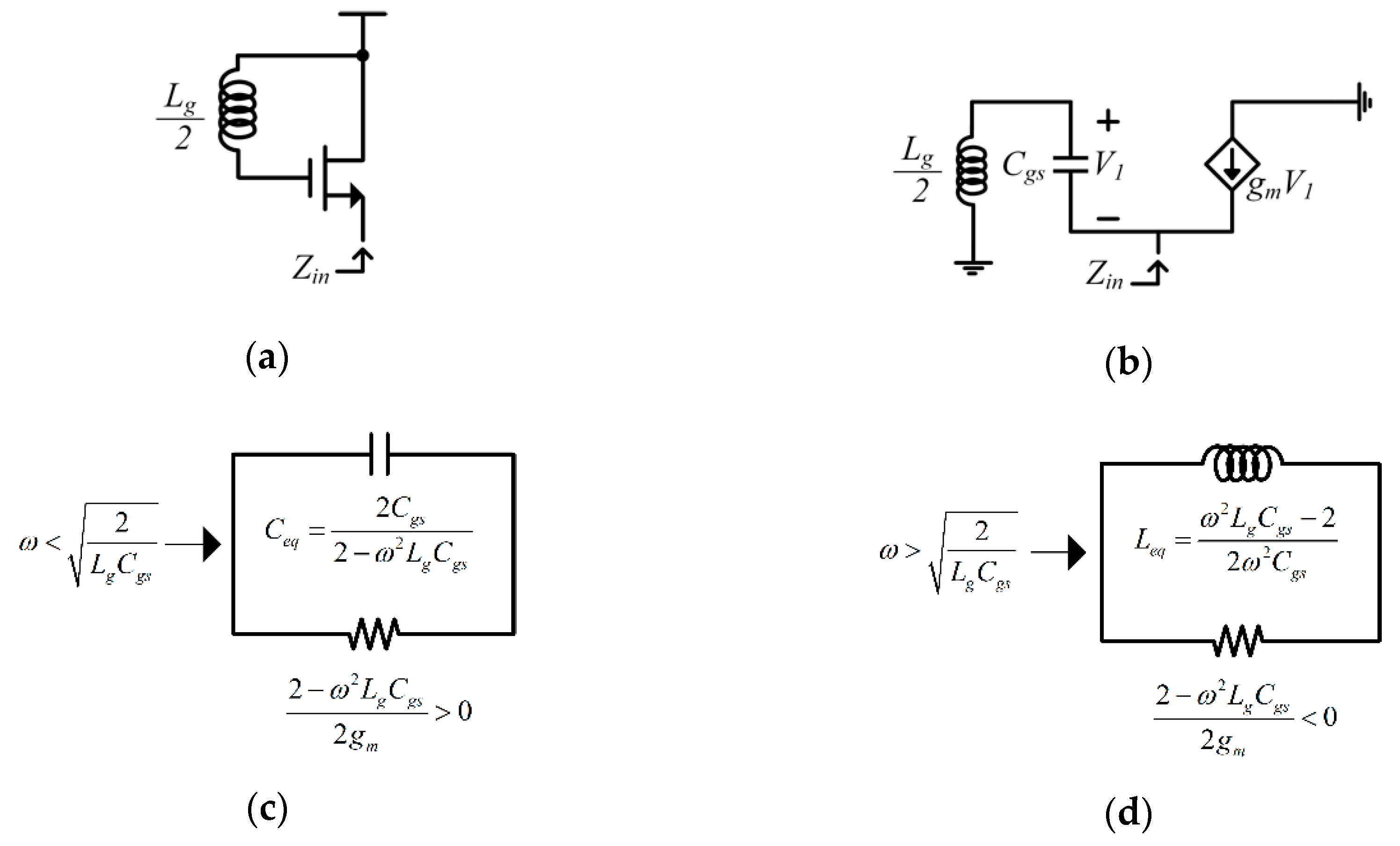
Figure 2a shows a half-circuit FSNR, so the inductance value of the
Lg is half of
Lg in the proposed oscillator. The FSNR circuit provides a selective characteristic depending on the oscillation frequency [
12].
Figure 2b shows a small signal equivalent circuit of the half-circuit FSNR. A parasitic capacitance
Cgs and a dependent current source
gmV1 are the only components accounted for in the small-signal equivalent circuit of a transistor to simplify the analysis and to obtain meaningful and tractable equations. The calculation of the input impedance looking at the source terminal of the transistor of the half circuit FSNR is based on the small-signal equivalent circuit in
Figure 2b. The calculated input impedance of this circuit has two solutions. When the oscillation frequency of oscillator
ω is lower than
, the input impedance of the half circuit FSNR, shown in
Figure 2c, is equivalent to a capacitor in parallel with a lossy resistance. Due to the lossy resistance, the total equivalent negative resistance is decreased, so the output power is decreased. In contrast, when
, the input impedance of the half-circuit FSNR is equivalent to an inductor in parallel with a negative resistance as shown in
Figure 2d. The solution in the case of
is preferred because it provides a high oscillation frequency and a high output power that are crucial in the mm-wave oscillator design.
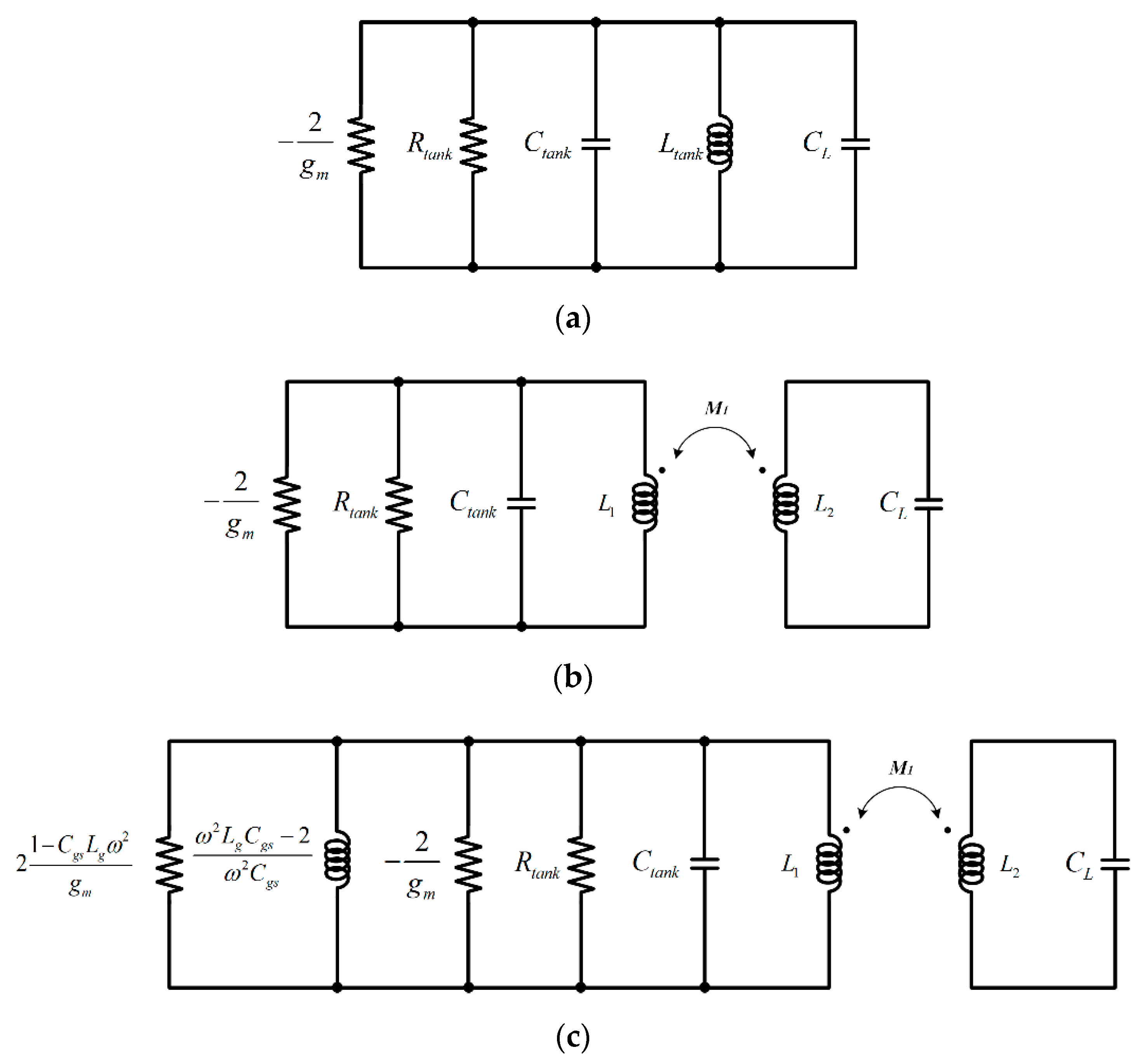
Figure 3 shows the small-signal equivalent circuits of the conventional XCO, the XCO with CLRC, and the proposed oscillator. From
Figure 3a, the oscillation frequency of the conventional XCO is:
where
Ltank is the total inductance value of the oscillator tank,
Ctank is the total capacitance value of the oscillator tank, and
CL is the total load capacitance. From
Figure 3b, the oscillation frequency of the XCO witch CLRC is:
where
L1 is the total inductance value of the oscillator tank,
L2 is the total inductance value at the gate of the buffer transistor, and mutual conductance
with
k1 being the coupling factor between
L1 and
L2. From
Figure 3c, the oscillation frequency of the proposed oscillator is:
where
, and
Cgs is the gate-source capacitance of transistors (M
5–M
6),
Lg is the inductor at the gate terminal of transistors (M
5–M
6).
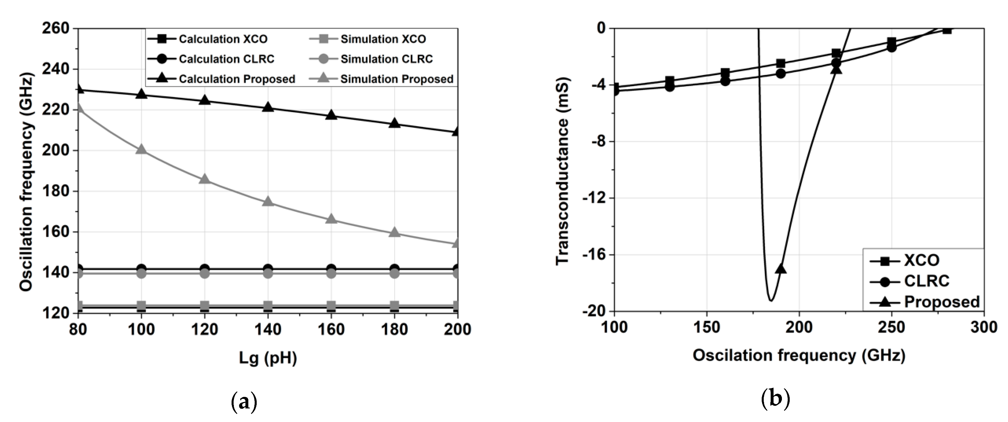
Figure 4a shows the calculated oscillation frequencies of three topologies shown in
Figure 1 versus
Lg from Equations (1)–(3) with
gm = 8 mS,
Ctank =
CL = 10 fF,
Cgs = 9 fF,
Ltank =
L1 =
L2 = 40 pH, and
M1 = 20 pH. In
Figure 4a, the oscillation frequency of the proposed oscillator decreases with an increase of
Lg. As can be seen in
Figure 4a, the oscillation frequency of the proposed oscillator is 230 GHz at
Lg = 80 pH which is 62% and 87% higher than the oscillation frequency of the XCO with CLRC (142 GHz) and the conventional XCO (123 GHz), respectively. The circuit simulation was also carried out to verify the validity of the theory and the simulation results are plotted in
Figure 4a. A BSIM4 model transistor was used in the circuit simulation. The simulation results agree with the theory equation about the trend of the oscillation frequency of the prosed oscillator with the change of
Lg. The simulated oscillation frequency of the proposed oscillator is lower and decreases more rapidly than the calculated oscillation frequency. This discrepancy is due to the simplification in the small-signal equivalent model of transistor. Nonetheless, the simulation results still show that the proposed oscillator has a higher oscillation frequency than that of the others, overall, in the simulated range of
Lg. To operate around 200 GHz, an inductance value smaller than 100 pH of
Lg was selected.
Moreover, the proposed oscillator has a better start-up condition and output power than those of the conventional XCO and the XCO with CLRC. The negative resistance of the conventional XCO and the XCO with CLRC is −2/
gm while that of the proposed oscillator is −2/
gm‖2(1−
CgsLgω2)/
gm. An additional negative resistance 2(1−
CgsLgω2)/
gm generated from the FSNR circuit gives rise to a better start-up condition and higher output power in the proposed oscillator. The circuit simulation was performed to verify the negative conductance improvement of the proposed oscillator. The simulated negative conductance of three structures with an identical oscillation frequency of 200 GHz is shown in
Figure 4b. At 200 GHz target frequency, the negative resistance of the conventional XCO and XCO with CLRC is −2.2 mS and −2.9 mS, respectively, whereas the negative resistance of the proposed oscillator is −11.3 mS, as shown in
Figure 4b. Therefore, the negative resistance of the proposed oscillator is almost 4 times higher than that of the XCO with CLRC, and five times higher than that of the conventional XCO.
Passive devices are designed and simulated using the HFSS electromagnetic simulation tool.
Figure 5 shows the passive devices of the proposed oscillator. Passive devices are implemented at two top metal layers that are a UTM metal layer with a thickness of 3.3 μm and a thick metal layer with a thickness of 0.9 μm. The CLRC transformer is implemented as a coplanar structure on the UTM metal to obtain a high Q-factor, where the Q-factor of
L1 is 35 and Q-factor of
L2 is 43. When the space between the primary inductor
L1 and secondary inductor
L2 is 3 μm, the coupling factor
k1 is 0.4. The gate inductor
Lg is also implemented on the UTM metal layer with an inductance value of 88 pH and a Q-factor of 34. The DTS transformer is implemented as a vertical stack structure to maximize the coupling factor, and, thus, the DTS transformer has a high coupling factor
k2 of 0.73. A capacitor with the capacitance value of 5 fF is implemented at the output port of the DTS transformer to maximize the output power transferred to the output load.
3. Measurement Results
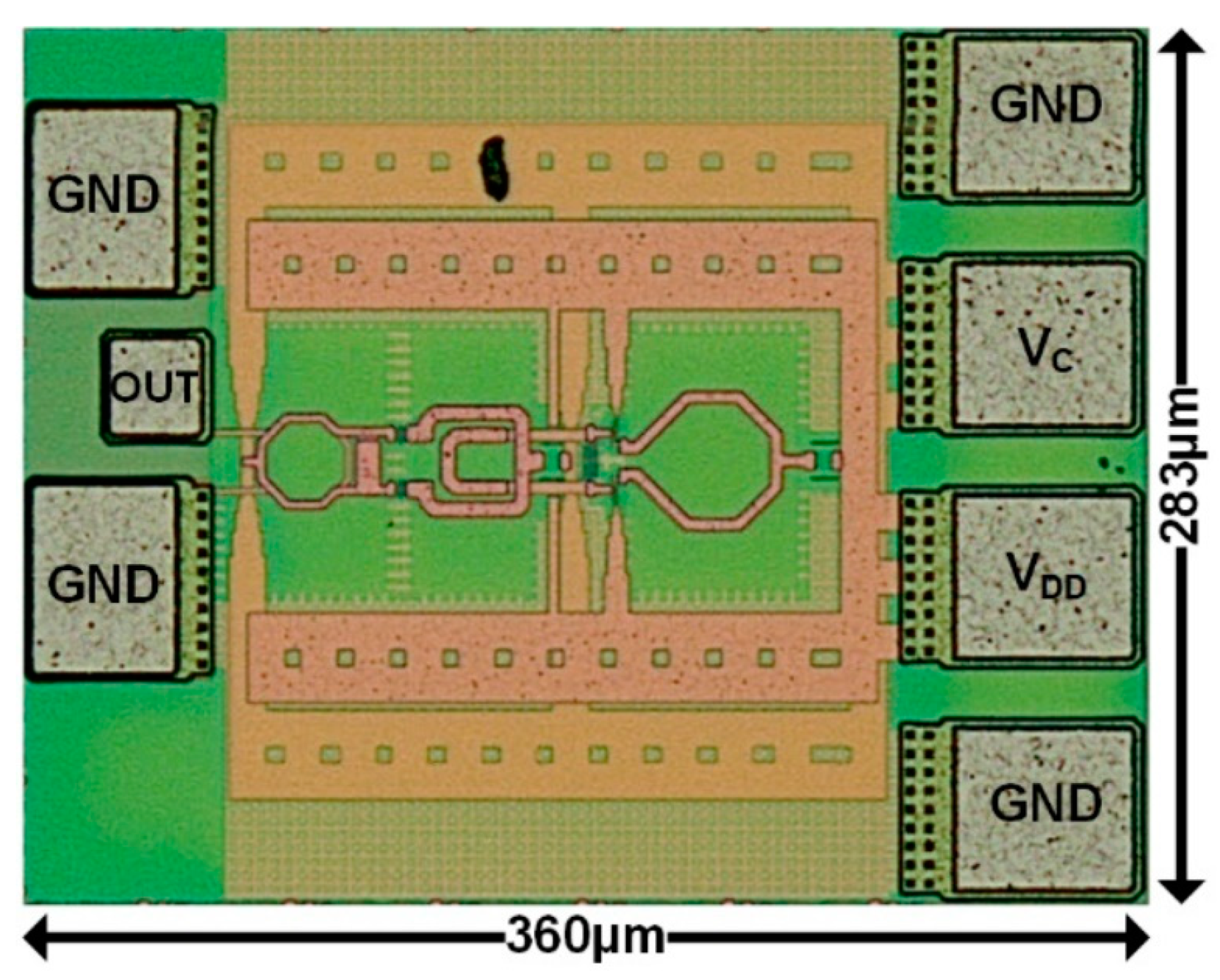
The proposed oscillator is fabricated in a 65 nm bulk CMOS process.
Figure 6 shows the implemented chip micrograph of the proposed oscillator with an area including pads of 360 × 283 μm
2. The area of the output pad is designed smaller than the power pads (
VDD and
VC) and ground pads (GND) to minimize parasitic capacitance and loss due to coupling with the lossy substrate.
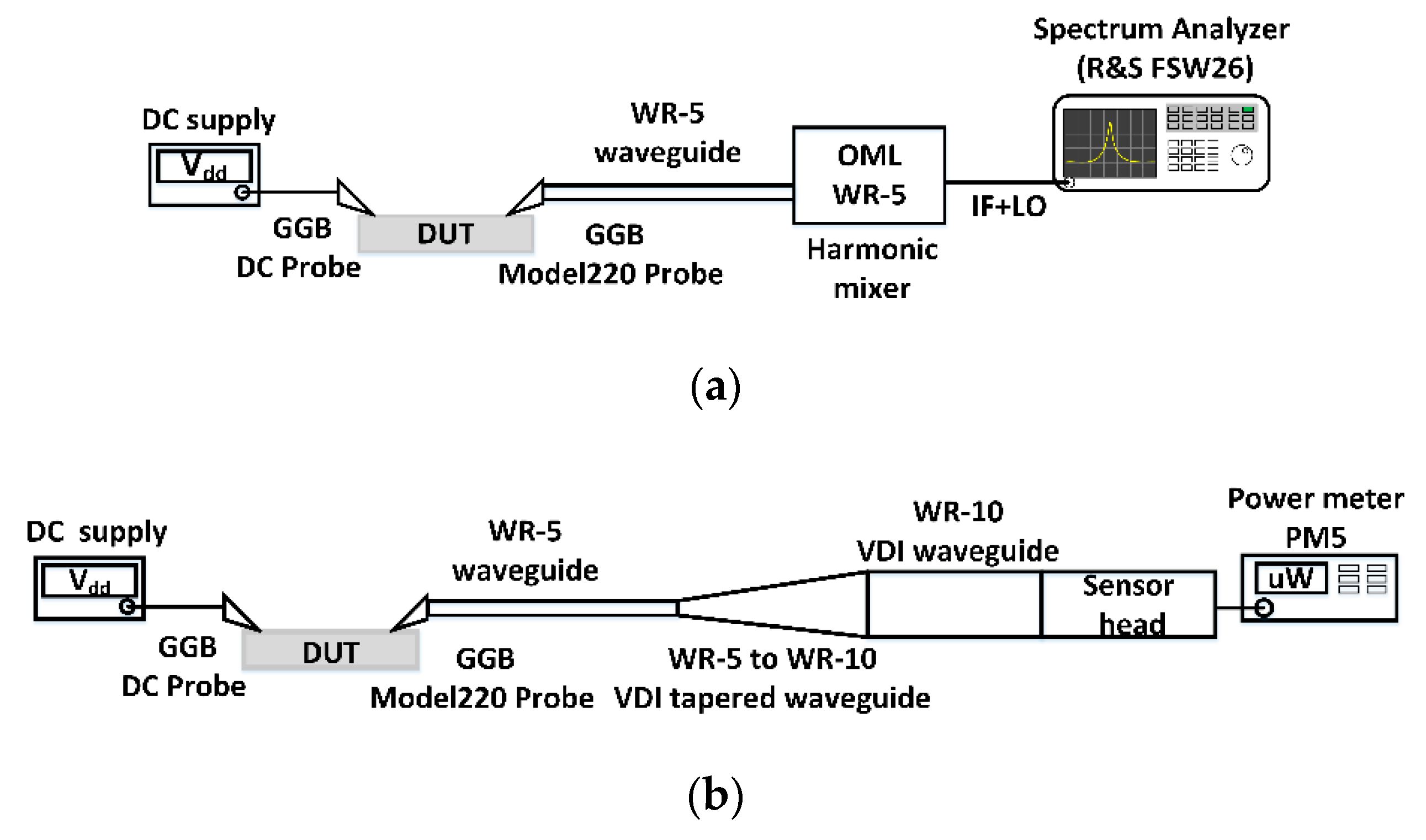
The output spectrum of the proposed oscillator was measured based on the measurement setup using the spectrum analyzer, as shown in
Figure 7a. A GGB DC Probe was connected to the power pads of the fabricated chip. The GGB DC probe with a GPPG pin configuration provided two paths to supply two different DC voltage levels to operate the fabricated circuit. The output pads were connected to a GGB model 220 probe with GSG pin configuration to sense the output power. Then the output power was conducted through the WR-5 waveguide to an OML WR-5 harmonic mixer. At the harmonic mixer, the output signal from the proposed oscillator was down-converted by mixing it with a LO signal generated from an R&S FSW26 spectrum analyzer. The down-converted output signal from the harmonic mixer was received, and the oscillation frequency was automatically calculated, by the R&S FSW26 spectrum analyzer.
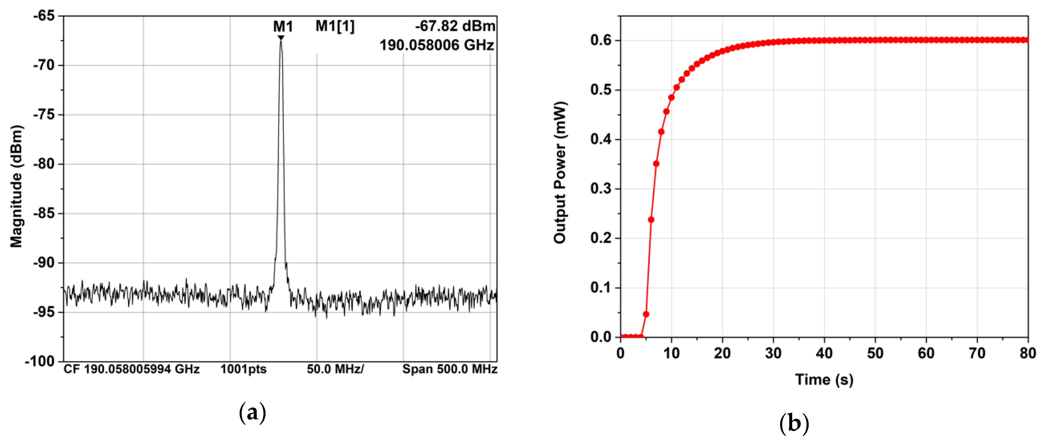
Figure 8a shows the measured oscillation frequency of 190 GHz.
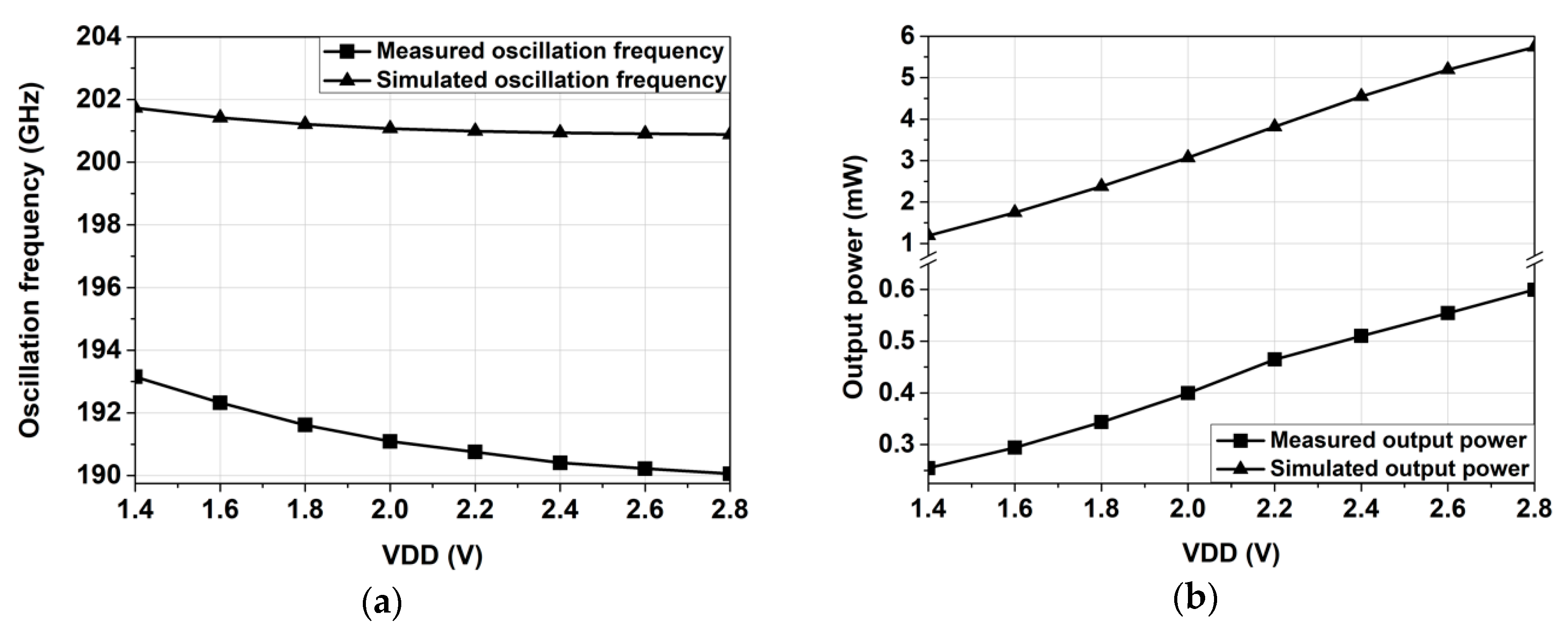
Figure 9a shows the effect of voltage supply on oscillation frequency. The measurement result shows that the oscillation frequency changed from 193.1 to 190.1 GHz when
VDD was increased from 1.4 to 2.8 V. At
VDD = 2.8 V, the measured oscillation frequency was 10 GHz lower than the simulated oscillation frequency because of the extrapolation model of active devices at mm-wave frequency range.
The output power of the fabricated proposed oscillator was measured by the measurement setup using a power meter, as shown in
Figure 7b. The output power was transferred to a power meter PM5 through a GGB model 220 probe, a WR-5 waveguide, a WR-5 to WR-10 VDI tapered waveguide, a WR-10 VDI waveguide, and a sensor head. The total transmission loss from the probe to the WR-10 VDI waveguide was 5.1 dB. The output power level was calculated by a PM5 power meter.
Figure 8b shows the highest measured output power was 0.6 mW or −2.2 dBm at
VDD = 2.8 V and
VC = 1 V. At
VDD = 2.8 V, the voltage across each transistor was approximately 1.4 V because of the stack structure.
Figure 9b shows the effect of voltage supply on output power. The measured output power increased from 0.254 to 0.6 mW and the simulated output power increased from 1.1 to 5.9 mW when
VDD increased from 1.4 to 2.8 V. The large discrepancy between the measured output power and the simulated output power was due to the extrapolation model of active devices at mm-wave frequency range.
Table 1 shows the performance comparison of this work with the previous state of the art. The proposed oscillator generates a competitive output power at a high fundamental frequency with a compact chip area. Though the power consumption of the proposed oscillator is higher than that of the oscillator in [
25], the output power of the proposed oscillator is 0.8 dB or 17% higher than the output power of the oscillator in [
25]. This is a worthy trade-off in designing an mm-wave CMOS oscillator.


