Article

Effect of the High-Temperature Off-State Stresses on the Degradation of AlGaN/GaN HEMTs

Key Laboratory for Wide Band Gap Semiconductor Materials and Devices of Education, The School of Microelectronics, Xidian University, Xi’an 710071, China
*
Author to whom correspondence should be addressed.
Electronics 2019, 8(11), 1339; https://doi.org/10.3390/electronics8111339
Submission received: 21 October 2019 / Revised: 5 November 2019 / Accepted: 11 November 2019 / Published: 13 November 2019
(This article belongs to the Section Microelectronics)

Abstract

:
GaN-based high electron mobility transistors offer high carrier density combined with high electron mobility and often require operation at high frequencies, voltages, and temperatures. The device may be under high temperature and high voltage at the same time in actual operation. In this work, the impact of separate off-state stresses, separate high-temperature stresses, and off-state stresses at high temperatures on AlGaN/GaN high electron mobility transistors (HEMTs) grown on Si substrates was investigated. The output current and gate leakage of the device degenerated to different degrees under either isolated off-state or high-temperature stress. The threshold voltage of the device only exhibited obvious negative drift under the action of high-temperature and off-state stresses. The parameter at high temperature (or room temperature) before stress application was the reference. We found that there was no significant difference in the degradation rate of drain current and transconductance peak when the same off-state stress was applied to the device at different temperatures. It was concluded that, under the high-temperature off-state electric field pressure, there were two degradation mechanisms: one was the inverse piezoelectric polarization mechanism only related to the electric field, and the other was the degradation mechanism of the simultaneous action of temperature and electric field.

1. Introduction

GaN-based high electron mobility transistors (HEMTs) are excellent candidates for high-frequency, high-field, and high-temperature applications in the microwave range, due to their large band gap, high breakdown electric field, and high mobility two-dimensional electron gas (2DEG) [1,2,3]. On the one hand, high-field degradation characteristics refer to the possible degradation effect of AlGaN/GaN HEMT devices after the application of the enhanced electric field. At present, the primary explanation for the degradation of AlGaN/GaN HEMT devices under strong electric field stress is the thermionic electron effect. The thermionic electron will lead to the capture and generation of surface state traps between the gate and drain, thus affecting the performance of devices and causing device degradation. Some studies believe that the inherent traps [4,5] will capture the thermal electrons, while others believe that the thermal electrons themselves will form new defects [6,7,8,9]. Actually, the thermionic electron effect could not be used to explain all of the high-field degradation phenomena. The device lacks channel thermal electrons under the off-state stress of the large electric field. The experimental results show that the device will also degrade under off-state stress [10,11]. It is suggested that there may be other mechanisms for degradation of the device under off-state stress.
John et al. [12] proposed a new degradation mechanism hypothesis for this phenomenon—the inverse piezoelectric polarization effect. At a high electric field, the expansion of the barrier layer caused by the inverse piezoelectric effect leads to lattice relaxation and defects. However, it is undeniable that the same stress conditions will have different effects on different process technologies and structural devices, and the internal mechanisms may be different. Therefore, it still requires a lot of research to grasp the mechanism of high-field degradation fully.
On the other hand, the high temperature resistance of GaN materials determines that AlGaN/GaN HEMT devices are often used in high-temperature environments [13,14,15]. Therefore, it is necessary to study the reliability of devices during high-temperature operation. In past research on device reliability, the experiments of temperature change characteristics [15,16,17,18,19] and high-field stress [4,5,6,7,8,9,10,11,12] were separately performed, which is different from the current situation where the device is operated in a high-temperature environment. Therefore, this paper studied the electrothermal coupling degradation characteristics of AlGaN/GaN HEMT devices.
We studied the degradation of the sample device under separate off-state stresses, separate high-temperature stresses, and off-state stresses at high temperatures, in order to compare and study the parameter changes of the device when the temperature stress and the electric stress existed at the same time, and analyze the cause of the change.

2. Materials and Methods

The AlGaN/GaN HEMT device used in this experiment adopted a standard process. The AlGaN/GaN heterojunction structure was grown by metal–organic chemical vapor deposition (MOCVD) on SiC substrates. Both the GaN buffer layer (2 µm) and the AlGaN layer (25 nm) were unintentionally doped. The Al composition in the AlGaN barrier layer was 30%. Standard Ti/Al/Ni/Au (20 nm/140 nm/55 nm/45 nm) source/drain ohmic metallization was annealed at 850 °C for 30 s and a rectangular-shaped Ni/Au gate contact was used. This was followed by the deposition of 60 nm and 200 nm plasma-enhanced chemical vapor deposition (PECVD) Si3N4 passivation layer, respectively.
For the off-state high-power stress, the source was held at ground level while the applied stress conditions consisted of a VGstress = −3 V and VDstress = 30 V. Following this, the device was turned off, the channel was left unopened, and the stress time was 6000 s. After stress, the device was left stationary for 72 h to restore. We measured the characteristics by using an Agilent B1500A device analyzer and a cascade probe station. Then, in the high-temperature experiment, the device was heated by a DHG-9033BS-III electrothermal constant temperature blast drying oven. The test sample was first placed at room temperature for testing then placed in the thermostatic chamber. The temperatures were set to 50, 75, and 100 °C, in sequence. In order to make sure that the temperature of the device was uniform before measurement, the sample was stored for two minutes after the oven reached the preset temperature. Finally, the most important study was the degradation characteristics of AlGaN/GaN HEMT devices after applying off-state stress at different ambient temperatures. The experimental samples, test methods, and stress conditions used were the same as before. During the experiment, the three sets of devices were placed at ambient temperatures of 50, 75, and 100 °C.

3. Results and Discussion

3.1. Off-State Stress

A characteristic curve comparing reference, off-state stress condition, and recovery condition is shown in Figure 1. It can be seen from the transfer characteristic curve of Figure 1a that, after stress, the maximum transconductance and drain of the device current decreased. Among them, the threshold voltage was unchanged, the maximum transconductance Gmmax was reduced by 24.9%, and the maximum drain current was reduced by 31%. Nevertheless, the transfer characteristic curve of the device was restored to the pre-stress level after the device was static for 72 h. This phenomenon is generally attributed to the fact that, after stress, the electrons of the device—under the action of a strong electric field—obtain enough energy and enter the AlGaN barrier layer or the device surface to be captured by traps [7]. Thus, the concentration of 2DEG in the channel decreased, which was macroscopically shown as the decrease of output leakage current of the device. The degradation of the characteristic curve was due to the inherent trapped carriers in the device. After storing the sample for a while to recover, the trap released the trapped carrier and the device characteristics were restored to the pre-stress level.
Figure 1b shows the variation of the gate leakage current curve of the device. It can be seen that, after stress, the gate leakage current increased by nearly two orders of magnitude. This may be because the electric field direction generated by the negative gate voltage acting on the AlGaN barrier layer is the same as that of the AlGaN polarization electric field, and the two electric fields interact with each other [6,20]. As a result, the barrier layer of AlGaN was subjected to a more significant tensile stress, which stretched the lattice structure and produced new defects in the material. The new trap-assisted carrier tunneling passed through the AlGaN barrier layer and formed a new gate current leakage channel—that is, the gate leakage current of AlGaN/GaN HEMT devices increased after stress. Moreover, the gate leakage current was unrecovered, which was consistent with the post-stress curve. It is further indicated that new traps introduced under off-state stress caused the gate leakage channel and these new defects could not be recovered with the removal of stress.

3.2. High-Temperature Stress

Figure 2 shows a representative curve of the DC characteristics of AlGaN/GaN HEMT devices at different ambient temperatures. It can be seen intuitively from Figure 2a that, as the ambient temperature increased, the transconductance peak and drain current of the device continuously decreased. The threshold voltage had slightly negatively drifted but the change was not obvious. The main reason was the decrease of the carrier saturation velocity in the high-temperature environment [21].
Compared with the data at room temperature, the peak value of the transconductance of the device decreased by 3.52% at 50 °C, 8.60% at 75 °C, and 13.47% at 100 °C. In terms of drain current, the drain current dropped by 3.32% at 50 °C, 8.34% at 75 °C, and 12.34% at 100 °C. In summary, taking the transconductance peak and drain current of the device as the ordinate, and the ambient temperature as the abscissa, the curve of the DC parameter of the device as a function of temperature was obtained (Figure 3). The inset was the degradation rate of the transconductance peak and drain current relative to room temperature at 50–100 °C. It can be seen that the transconductance peak and drain current of the device decreased linearly with the increase of the ambient temperature, and the degradation rate was also approximately linear with the ambient temperature. It shows that the DC characteristics of the device degraded uniformly with increasing temperature. From the gate leakage current characteristics of the device in Figure 2b at different ambient temperatures, it can be seen that the gate leakage current of the device did not change significantly with the increase of the ambient temperature. It can be considered that the Schottky junction of the experimental sample used is highly reliable, and remains substantially stable over this temperature range. After the device returned to room temperature, the transfer characteristic curve returned to its original level. The carrier saturation velocity of the device was constant at the same temperature. This further indicates that the decrease of drain current at high temperature is mainly due to the decrease of carrier saturation velocity.

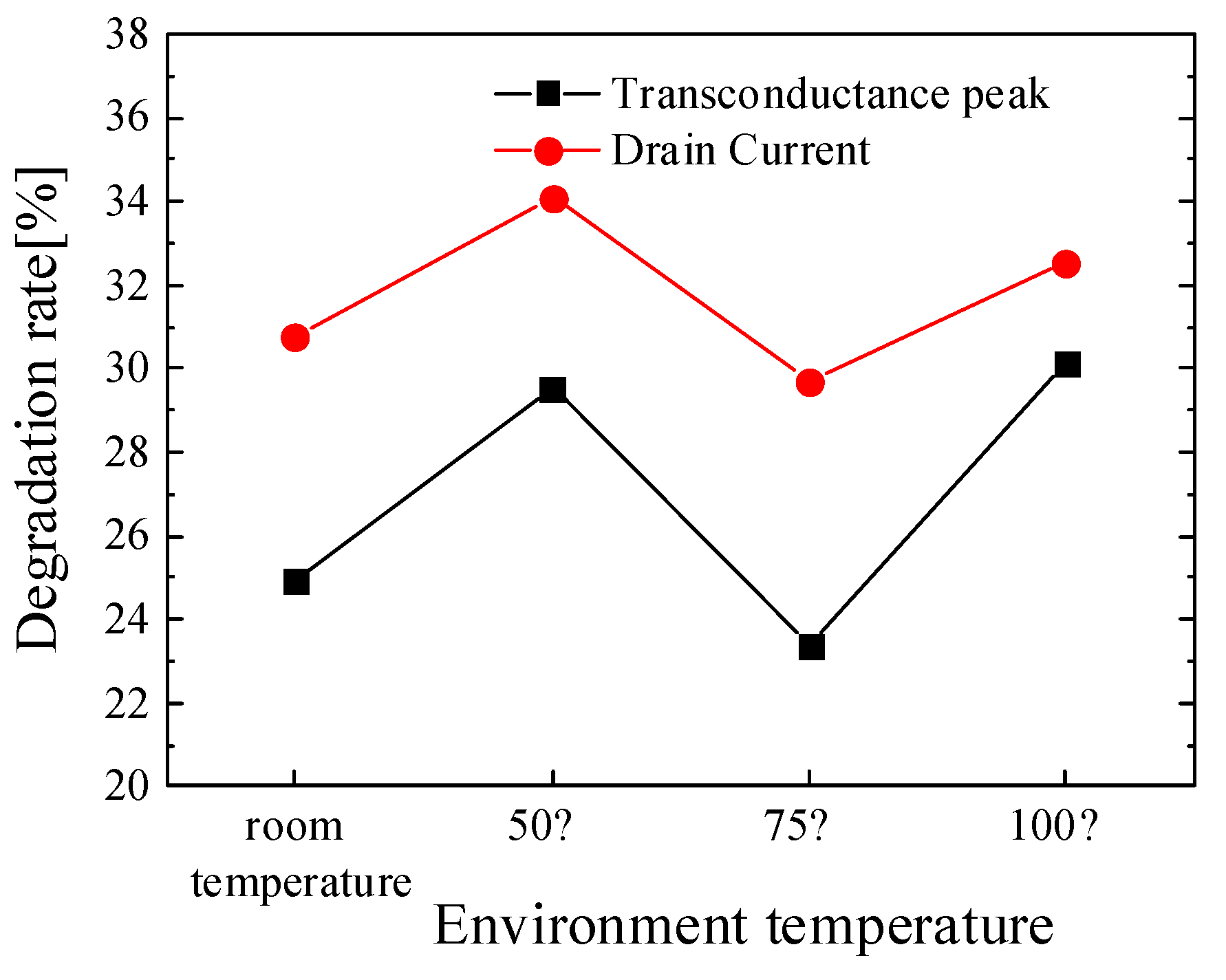
3.3. Off-State Stress at High Temperature

In this section, the experimental results at 75 °C are taken as an example. The direct current characteristics of the device at room temperature, the high-temperature environment before stress application, the high-temperature environment after stress application, the return to room temperature, and the static condition for 72 h were compared. After applying the off-state stress at 75 °C, one reduced the temperature to room temperature without any stress and stored the sample. These were considered the static conditions. Then, the experimental results at different ambient temperatures were statistically analyzed to investigate the effect of temperature on the off-state stress degradation characteristics.
As can be seen in Figure 4a, the device transfer and transconductance characteristics after 75 °C application of off-state stress were significantly degraded compared to the initial measurement at room temperature. Individually, when the ambient temperature rose to 75 °C, the drain current and transconductance peak of the device decreased but the threshold voltage did not change significantly. This was consistent with the experimental results of the previous high-temperature characteristics mainly because the temperature caused a decrease in the two-dimensional electron gas mobility at the channel of the device. After applying the off-state stress at 75 °C, the drain current and transconductance peak of the device decreased further, and the threshold voltage showed a significant negative drift. The specific data is shown in Table 1, where the degradation rate of each parameter relative to the initial measured value is compared. It can be seen from the data that the main degradation occurred after application of the off-state stress. It can also be seen that the device had a significant recovery of drain current and transconductance peak after returning to room temperature. However, the threshold voltage recovery was not apparent, and no more replies could be achieved after 72 h of standing. In combination with Figure 2a, it can be seen that the threshold voltage of the device was only slightly negative at high temperature, which can be attributed to the increase of the density of 2DEG surface at high temperature. It led to a rise in the number of electrons consumed in the channel that required a higher negative bias to be exhausted. It shows that the current technology level can ensure the stability of metal contact of the device at this temperature. The degradation mechanism [18] of metal contact driven by ambient temperature is accelerated under the high electric field. In other words, the Schottky contact of the gate electrode begins to irreversibly degenerate under the double action of high temperature and high electric field [22]. According to V t h = ϕ B Δ E C q q N d d d 2 2 ε , when the height of the Schottky barrier ( ϕ B ) decreases, the threshold voltage ( V t h ) decreases.
Figure 4b shows a comparison of gate leakage current characteristics of AlGaN/GaN HEMT devices. It can be seen that there was no significant difference between the initial test and the test at 75 °C but the gate leakage current of the device after application of the off-state stress had increased significantly by more than two orders of magnitude. It is indicated that the off-state stress had a significant effect on the Schottky contact of the gate.
In order to analyze the effects of different ambient temperatures on the off-state stress degradation, the parameter degradation of the device at room temperature, 50, 75, and 100 °C was statistically analyzed. Based on the parameters at high temperature (or room temperature) before stress application, the degradation rate of the device parameters after applying the off-state stress at different temperatures was calculated. The results are shown in Figure 5. It can be seen that there was no apparent law between the degradation rate of the device drain current and the transconductance peak and the temperature. This is because the degradation of the device under off-state stress is a high-field-driven inverse piezoelectric polarization mechanism. This mechanism is driven by an electric field rather than current, and the ambient temperature does not have a significant effect on the applied electric field. Therefore, it does not contribute to degradation under the off-state stress of the device.
At the same time, it can be seen from Table 1 that the recovery characteristics of the experimental samples subjected to the off-state stress at high temperature were poor. Although the drain current and transconductance of the device had recovered, there was still a large gap between the values before the experiment. The gate leakage current and the threshold voltage were substantially unrecovered. By comparing the device recovery characteristics at room temperature, it can be seen that the degradation of the device was not only the reverse piezoelectric polarization mechanism mentioned above but also a mechanism in which both temperature and voltage produced effects. In addition to the influence on the Schottky contact described above, there may have also been an influence on the AlGaN/GaN interface layer. It has been proved that in the process of reverse gate bias, the AlGaN/GaN interface trap captures electrons in the channel and causes the negative shift of threshold voltage [9]. At high temperature, the interface structure of AlGaN/GaN is unstable, which is easy to generate more interface traps. Therefore, the severe negative drift of the device threshold voltage at the high electric field and high temperature may be the result of the degradation of both the Schottky and AlGaN/GaN interface. Moreover, the source–drain current was reduced, and the deterioration of both mechanisms was irreversible.

4. Conclusions

The off-state stress was applied to the AlGaN/GaN HEMT at different ambient temperatures in order to study electrothermal coupling reliability. The experimental results show that the increase of ambient temperature lead to the decrease of the drain current and the transconductance peak of the device. The decrease rate varied uniformly with the temperature and this could be restored when the device came back to room temperature. The main reason was the decrease of 2DEG mobility in the high-temperature environment. The degradation mechanism of the device consisted of two parts, one of which was the inverse piezoelectric polarization effect only related to the electric field. There was no obvious relationship between the degradation rate of drain current and the peak transconductance and temperature. It was because the drain current degradation of the device under the in-state stress as the inverse piezoelectric polarization mechanism driven by the electric field. This mechanism as driven by electric field rather than current, and the ambient temperature had no visible effect on the applied electric field, so it did not affect the degradation of devices under the off-state stress. It led to recoverable leakage current and unrecoverable gate leakage degradation. The other was the degradation mechanism of the simultaneous action of temperature and electric field. It did not only cause the unrecoverable degradation of the leakage current but also made the unrecoverable threshold voltage shift negatively.

Author Contributions

Conceptualization, J.L.; validation, M.L.; formal analysis, J.L.; investigation, C.L. and J.L.; resources, L.W.; writing—original draft preparation, J.L.; writing—review and editing, J.L.; visualization, J.L.; supervision, S.W.; project administration, S.W.; funding acquisition, H.L.

Funding

This research is supported by the National Natural Science Foundation of China (Grant Nos.61376099, 61434007, and 61504100) and the Major Fundamental Research Program of Shaanxi (Grant No.2017ZDJC-26).

Conflicts of Interest

The authors declare no conflict of interest.

References

  1. Pengelly, R.S.; Wood, S.M.; Milligan, J.W. A review of GaN on SiC high electron-mobility power transistors and MMICs. IEEE Trans. Microw. Theory Tech. 2012, 60, 1764–1783. [Google Scholar] [CrossRef]
  2. Akita, M.; Kishimoto, S.; Mizutani, T. High-frequency measurements of AlGaN/GaN HEMTs at high temperatures. IEEE Electron Device Lett. 2001, 22, 376–377. [Google Scholar] [CrossRef]
  3. Palacios, T.; Chakraborty, A.; Rajan, S. High-power AlGaN/GaN HEMTs for Ka-band applications. IEEE Electron Device Lett. 2005, 26, 781–783. [Google Scholar] [CrossRef]
  4. Kim, H.; Tilak, V.; Green, B.M. Reliability Evaluation of High Power AlGaN/GaN HEMTs on SiC Substrate. Phys. Status Solidi 2001, 188, 203–206. [Google Scholar] [CrossRef]
  5. Valizadeh, P.; Pavlidis, D. Effects of RF and DC stress on AlGaN/GaN MODFETs: A low-frequency noise-based investigation. IEEE Device Mater. Reliab. 2005, 5, 555–563. [Google Scholar] [CrossRef]
  6. Makaram, P.; Joh, J.; Jesús, A.D.A. Evolution of structural defects associated with electrical degradation in AlGaN/GaN high electron mobility transistors. Appl. Phys. Lett. 2010, 96, 756–758. [Google Scholar] [CrossRef]
  7. Joh, J.; Alamo, J.A.D. A Current-Transient Methodology for Trap Analysis for GaN High Electron Mobility Transistors. IEEE Trans. Electron Devices 2011, 58, 132–140. [Google Scholar] [CrossRef]
  8. Omar, C.; Loic, T.; Alain, B. Effect of HTRB lifetest on AlGaN/GaN HEMTs under different voltages and temperatures stresses. Microelectron. Reliab. 2018, 88–90, 402–405. [Google Scholar]
  9. Malik, A.; Sharma, C.; Laishram, R. Role of AlGaN/GaN interface traps on negative threshold voltage shift in AlGaN/GaN HEMT. Solid-State Electron. 2018, 142, 8–13. [Google Scholar] [CrossRef]
  10. Douglas, E.A.; Chang, C.Y.; Cheney, D.J. AlGaN/GaN High Electron Mobility Transistor degradation under on- and off-state stress. Microelectron. Reliab. 2011, 51, 207–211. [Google Scholar] [CrossRef]
  11. Rong, J.; Xiao, S.; Jingtian, F. Multiple Defects Cause Degradation After High Field Stress in AlGaN/GaN HEMTs. IEEE Trans. Device Mater. Reliab. 2018, 18, 364–376. [Google Scholar]
  12. Joh, J.; Del, A. A model for the critical voltage for electrical degradation of GaN high electron mobility transistors. Microelectron. Reliab. 2010, 50, 767–773. [Google Scholar] [CrossRef]
  13. Darwish, A.M.; Bayba, A.J.; Hung, H.A. Thermal resistance calculation of AlGaN-GaN devices. IEEE Trans. Microw. Theory Tech. 2004, 52, 2611–2620. [Google Scholar] [CrossRef]
  14. Oxley, C.H.; Uren, M.J.; Coates, A. On the temperature and carrier density dependence of electron saturation velocity in an AlGaN/GaN HEMT. IEEE Trans. Electron Devices 2006, 53, 565–567. [Google Scholar] [CrossRef]
  15. Lee, J.M.; Min, B.G.; Ju, C.W. High temperature storage test and its effect on the thermal stability and electrical characteristics of AlGaN/GaN high electron mobility transistors. Curr. Appl. Phys. 2017, 17, 157–161. [Google Scholar] [CrossRef]
  16. Husna, F.; Lachab, M.; Sultana, M. High-temperature performance of AlGaN/GaN MOSHEMT with SiO2 gate insulator fabricated on Si (111) substrate. IEEE Trans. Electron Devices 2012, 59, 2424–2429. [Google Scholar] [CrossRef]
  17. Alim, M.A.; Rezazadeh, A.A.; Gaquiere, C. Temperature Effect on DC and Equivalent Circuit Parameters of 0.15-μm Gate Length GaN/SiC HEMT for Microwave Applications. IEEE Trans. Microw. Theory Tech. 2016, 64, 3483–3491. [Google Scholar] [CrossRef]
  18. Zhao, M.; Wang, X.; Liu, X. Thermal storage of AlGaN/GaN high-electron-mobility transistors. IEEE Trans. Device Mater. Reliab. 2010, 10, 360–365. [Google Scholar] [CrossRef]
  19. Omar, C.; Loic, T.; Eric, W. Temperature and voltage effects on HTRB and HTGB stresses for AlGaN/GaN HEMTs. In Proceedings of the 2018 IEEE International Reliability Physics Symposium, Burlingame, CA, USA, 11–15 March 2018. [Google Scholar]
  20. Meneghesso, G.; Meneghini, M.; Stocco, A. Degradation of AlGaN/GaN HEMT devices: Role of reverse-bias and hot electron stress. Microelectron. Eng. 2013, 109, 257–261. [Google Scholar] [CrossRef]
  21. Chang, Y.; Tong, K.Y.; Surya, C. Numerical simulation of current–voltage characteristics of AlGaN/GaN HEMTs at high temperatures. Semicond. Sci. Technol. 2015, 20, 188–192. [Google Scholar] [CrossRef]
  22. Sun, H.; Bajo, M.M.; Uren, M.J. Progressive failure site generation in AlGaN/GaN high electron mobility transistors under OFF-state stress: Weibull statistics and temperature dependence. Appl. Phys. Lett. 2015, 106, 7261. [Google Scholar] [CrossRef] [Green Version]
Figure 1. Different conditions of typical DC characteristic curves. (a) Transfer characteristic and transconductance characteristics; (b) gate leakage current.
Electronics 08 01339 g001
Figure 2. Typical DC characteristic curves at different temperatures. (a) Transfer and transconductance characteristics; (b) gate leakage current.
Electronics 08 01339 g002
Figure 3. The curve of the peak transconductance and drain current (VG = 0 V and VD = 5 V) to the ambient temperature.
Electronics 08 01339 g003
Figure 4. Typical DC characteristic curves at different conditions. (a) Transfer characteristic and transconductance characteristics; (b) gate leakage current.
Electronics 08 01339 g004
Figure 5. Degradation rate of device parameters caused by off-state stress at different temperatures.
Electronics 08 01339 g005
Table 1. Negative deviation rate of threshold voltage and degradation rate of transconductance peak and drain current.
Degradation Rate [%]Temperature of 75 °COff-state Stress Under 75 °CReturn to Room Temperature72 h to Recovery
Threshold voltage 1.7133.1526.5127.62
Transconductance peak 11.5232.2013.6111.26
Drain current (VG =1V /VD = 1 V)15.0040.2622.1118.68

