Article

Research on Linear Active Disturbance Rejection Control in DC/DC Boost Converter

1
College of Automation Engineering, Shanghai University of Electric Power, Shanghai 200090, China
2
School of Engineering and Built Environment, Griffith University, Gold Coast, QLD 4222, Australia
*
Author to whom correspondence should be addressed.
Electronics 2019, 8(11), 1249; https://doi.org/10.3390/electronics8111249
Submission received: 24 September 2019 / Revised: 28 October 2019 / Accepted: 28 October 2019 / Published: 31 October 2019
(This article belongs to the Section Power Electronics)

Abstract

:
This paper proposes a cascade control strategy based on linear active disturbance rejection control (LADRC) for a boost DC/DC converter. It solves the problem that the output voltage of boost converter is unstable due to non-minimum phase characteristics, input voltage and load variation. Firstly, the average state space model of boost converter is established. Secondly, a new output variable is selected, and a cascade control is adopted to solve the problems of narrow bandwidth and poor dynamic performance caused by non-minimum phase. LADRC is used to estimate and compensate the fluctuations of input voltage and loads in time. Linear state error feedback (LSEF) is used to achieve smaller errors than traditional control method, which ensures the stability and robustness of the system under internal uncertainty and external disturbance. Subsequently, the stability of the system is determined by frequency domain analysis. Finally, the feasibility and superiority of the proposed strategy is verified by simulation and hardware experiment.

1. Introduction

With the vigorous promotion of renewable energy such as photovoltaics and wind turbines, the DC microgrid has received extensive attention [1,2,3]. Compared with the AC microgrid, the DC microgrid has the advantages of high efficiency and simple control structure [4]. In addition, the DC microgrid avoids some of the problems in the AC microgrid. For instance, reactive power flow, harmonic current, and synchronization [5]. Therefore, the DC microgrid will become the main power architecture for buildings, parks, and power electronic loads. The instability of the output voltage will cause some problems, including protection device malfunction and damage to the electrical equipment, so it is important to ensure the stability of the DC output voltage.
In a DC microgrid, renewable energy units, loads, and other units are connected by inverters, such as DC/DC converters, DC/AC converters, AC/DC converters, etc. Moreover, it can be connected to the AC microgrid or the large grid through bidirectional DC/AC. Not only can the AC side disturbance and fault be effectively isolated, but also the DC side load can be reliably powered [6]. The DC/DC boost converter is an important part of the connection between each unit and the bus. It achieves voltage boost by a specific circuit structure and adjusting the on-off time of the switching device [7]. Open loop control is a simple method of controlling a step-up DC/DC converter that calculates the PWM pulse duty cycle from the input voltage and the output voltage. However, this method is extremely sensitive to external disturbances and changes from parameters. Moreover, it is easy to cause problems such as large overshoot of the output voltage and high amplitude of the inductor current. Therefore, most of the DC/DC converter control uses a closed-loop control method.
Scholars and researchers have done a lot of work on the control of DC/DC converters. In [8,9], the isolated converter is used to increase the output voltage by adjusting the turns ratio. However, the excessive number of turns leads to a large leakage inductor, which makes it difficult to improve the efficiency. In [10,11], a cascade converter is used, which can control the voltage by adjusting the duty ratio of the two parts of the switch tube, but the converter is inefficient and difficult to control. In [12], a high boost converter with a switched capacitor is proposed. High voltage gain is achieved at the appropriate duty cycle by introducing a switched capacitor into the switched mode DC-DC converter. However, the switched capacitor introduces a pulsating input current that can cause poor line and load regulation issues. In [13], state feedback control is adopted, which has strong suppression of load disturbance, but does not consider input voltage disturbance. In [14], the high-order synovial observer is used to estimate the load change in advance and cancel it in the feedforward channel, and combine it with the feedback control loop. It not only improves the transient characteristics of the system, but also improves the stability margin of the system. However, the calculation method of this method is too large and sensitive to noise.
By analyzing the transfer function of the step-up DC/DC converter, it can be seen that the system has a zero point in the right half plane. Capacitance voltage is directly controlled as an output, which causes the bandwidth to be narrowed and the dynamic performance of the system to deteriorate, which increases the control difficulty [15,16]. In [17], an input–output feedback linearization technique is proposed and applied to an AC/DC converter. In [18], an internal model control with a conditional integrator is proposed for the robust output regulation of a DC/DC buck converter. Due to the nonlinearity and unstable zero dynamics of the boost converter, a novel nonlinear control strategy based on input–output feedback linearization is proposed in [19]. In [20], a wide series of control techniques are presented for well-known power electronics converters, including the conventional DC-DC boost converter. In response to this problem, two main solutions can be obtained from the perspective of control and system: (1) changing the topology of DC/DC booster converter to eliminate the unstable zero dynamic; and (2) indirect control of the output voltage. By selecting a new output variable, the unstable zero dynamics of the converter are eliminated, and the relationship between the new output variable and the output voltage is used for control. The former directly controls the output voltage and easily satisfies the control effect, but increasing the power electronic switching device leads to an increase in cost. The latter does not change the topology of the converter, and the output voltage is controlled by indirect control, but the output voltage is susceptible to input voltage and resistance changes. The classical PI control relies on the error between the control target and the actual output to determine the control strategy to eliminate this error [21], so the design is simple and the applicability is good. However, this method designs the output feedback control according to the target error, so that the dynamic response characteristic is slow, and the system is adjusted only when the output has changed.
Based on the in-depth study of PID, active disturbance rejection control (ADRC) attributes all the uncertain factors acting on the controlled object to “unknown disturbances”, which are estimated and compensated by the extended state observer. This method is based on process error to reduce the error [22]. The active disturbance rejection control consists of three parts: tracking differentiator (TD), extended state observer (ESO), and nonlinear state error feedback (NLSEF) control law. To make the design of the controller simpler and easier to promote the application, Gao et.al. simplified the self-disturbance control to linear active disturbance rejection control (LADRC) [23].
The parameters’ setting of controller is simplified by using proportional-derivative (PD) control and establishing the proportional coefficient and differential time constant to the controller bandwidth [24]. Linearization of the ESO, conversion to a linear extended state observer (LESO), and the establishment of a link between the observer bandwidth and parameters, simplifies the design of the LESO. Since the active disturbance rejection controller does not depend on the system model and the algorithm is simple, it is applied in many fields. In [25], ADRC is applied to solve industrial problems. Industrial automation equipment was tested. In the worst case, performance improvement from just under 20% to 290% in all mechanical configuration was found. Coupled with the simplicity in the control algorithm itself, the ease of adjustment and operation, this improvement makes ADRC a viable alternative to existing industrial controller in manufacturing industry. In [26], from the perspective of uncertain system control, the main methods in modern control theory are sorted out, and the theoretical analysis of the main part of ADRC and the flexible application of ADRC method in specific problems are discussed. In [27], a fixed-time ADRC control method is proposed to solve the attitude control problem of the four-rotor unmanned aerial vehicle in the presence of dynamic wind, mass eccentricity and actuator fault. In [28], the LADRC method is applied in inverter control, which expands the range of virtual impedance and improves the immunity of the system. In [29], to improve the anti-interference ability of the speed control system, ADRC controller using phase-locking loop observer is proposed. In [30], ADRC is applied to the gyro control of micro-electro-mechanical systems, which not only drives the drive shaft to vibrate along a predetermined trajectory, but also compensates for manufacturing defects in a robust manner, making the performance of the gyro insensitive to parameter variations and noise. In [31], LADRC is proposed to be applied to a double-switch buck-boost converter. To ensure dynamic control performance and smooth switching in different operating modes, the model deviation in different working modes is regarded as a generalized disturbance, and a unified current control device can be derived for current controller design.
According to the above analysis, to solve the problem of output voltage instability caused by input voltage and load fluctuation and non-minimum phase of the DC/DC boost converter, this paper proposes a cascade control based on LADRC. Aiming at the instability of output voltage caused by the fluctuation of input voltage and load, and the change of system parameters, the LADRC is adopted to observe the fluctuation of voltage and load through the observer and eliminate it through the disturbance suppression channel. For the non-minimum phase problem of the system, a new output variable is selected to eliminate the unstable zero dynamics. The stability of the system is determined by frequency domain analysis. This control method can effectively eliminate the change of the output voltage caused by the renewable energy power generation unit and the load disturbance, and does not depend on the model of the system, the algorithm is simple, and is beneficial to engineering applications.
Through MATLAB/Simulink simulation analysis and experimental comparison with the control effect of PI controller, the results verify the effectiveness and superiority of the proposed control algorithm.

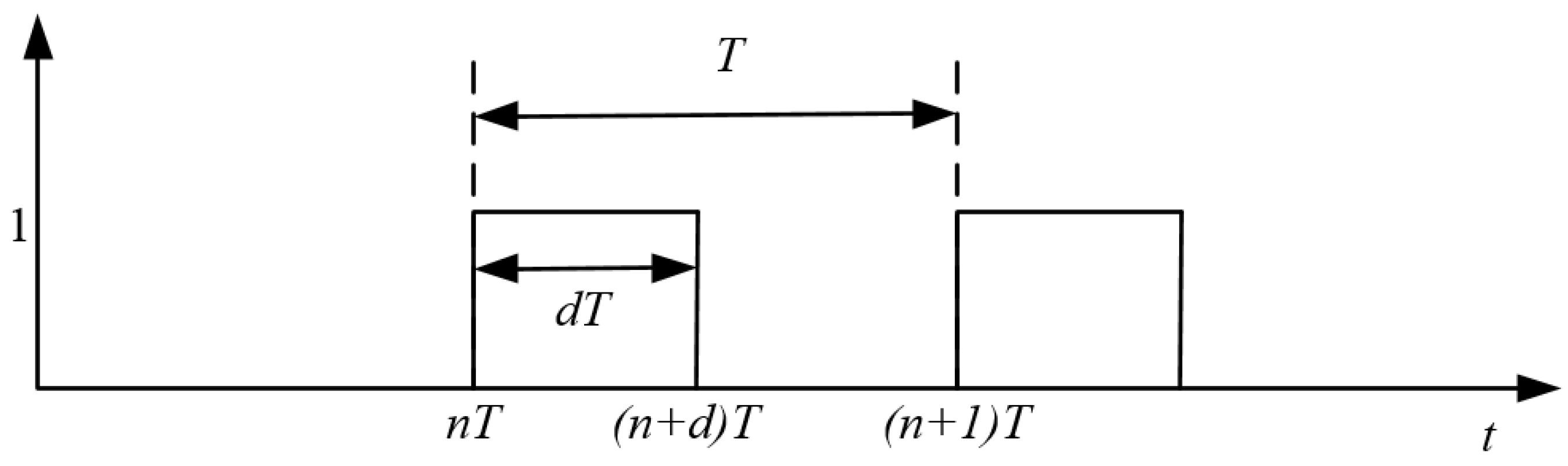
2. Modeling of DC/DC Boost Converter

Figure 1 shows a circuit diagram of a DC/DC boost converter. In the figure, Ui is the input voltage, IL is the inductive current, Uo is the output voltage, L is the inductance, C is the capacitance, and R is the resistive load.
The DC/DC boost converter uses PWM technology, which obtains the required output voltage by changing the duty cycle of the pulse. This paper introduces the pulse model integration method to establish the average model of the DC/DC boost converter. The waveform of switch function μ(t) is shown in Figure 2.
The pulse function μ(t) can be expressed as:
μ ( t ) = { 1 , n T < t ( n + d ) T 0 , ( n + d ) T < t ( n + 1 ) T
Switching frequency fsw is 10 kHz in this paper, where T =1/fsw is the switching period, d is the duty cycle, 0 < d < 1 and n = 0, 1, 2…
As can be seen from the above pulse function, the DC/DC boost converter has two operating states:
(1) Switch conduction mode, μ(t) = 1: When the switch is turned on, the input voltage Ui charges the inductor L, and the charging current is kept substantially constant. At the same time, the voltage of capacitor C supplies power to load R.
(2) Switch cutoff mode, μ(t) = 0: When the switch is turned off, the input voltage Ui and the inductor L together charge the capacitor C and supply power to the load resistor.
Switch conduction model equation:
{ L d I L d t = U i C d U o d t = 1 R U o
Switch cutoff model equation:
{ L d I L d t = U i U o C d U o d t = I L 1 R U o
The average mathematical model equations of the DC/DC boost converter can be obtained by combining Equations (2) and (3):
{ d I L d t = ( 1 d ) U o L + U i L d U o d t = ( 1 d ) I L C 1 R C U o

3. Control Method Design

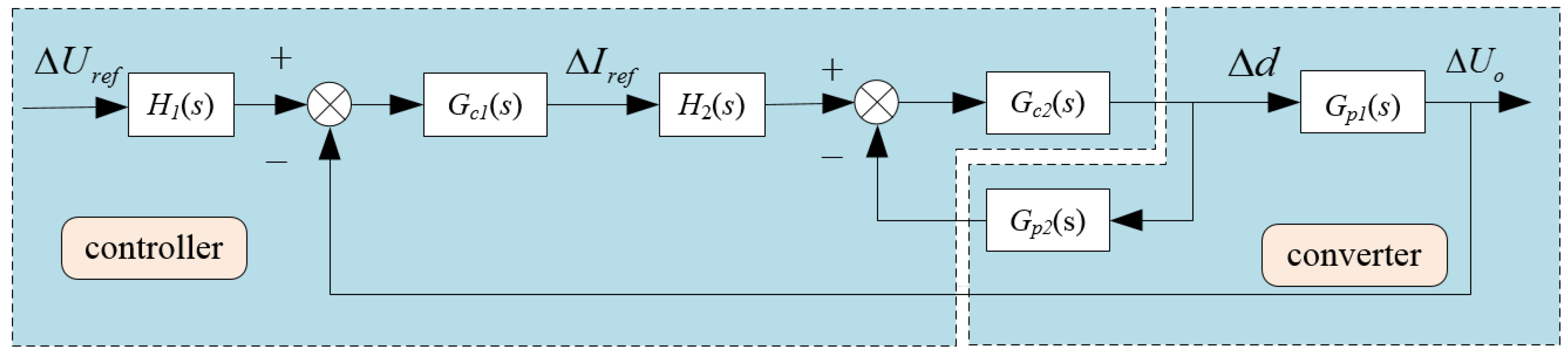
3.1. Cascade Control

According to the analysis of Equation (4), when the output voltage is directly controlled, the system is a non-minimum phase system. This will lead to narrow bandwidth and slow dynamic response to the system, which increases the difficulty of control. The output redefinition method is one of the methods to solve the non-minimum phase problem. By selecting a new output variable, a new output function is established, so that the zero dynamic subsystem is stable.
For the control of the DC/DC boost converter, a new output variable can be selected to eliminate the unstable zero dynamics and achieve the effect of change the non-minimum phase characteristics of the system. According to the model in Equation (4), if the inductor current is the system output, the new subsystem is the minimum phase system. Therefore, the output voltage control problem of the system can be converted into an inductor current control problem. Further consideration is given to how to achieve the desired output voltage value by controlling the inductor current. There is a relationship between the output voltage and the inductor current, can be written as:
I L ( ) = U o 2 ( ) / R U i
where IL(∞) and Uo(∞) are the steady state values of IL and Uo, respectively.
It can be seen from Equation (5) that the control of the output voltage can be achieved by controlling the inductor current. If the desired voltage is known, the reference value of the inductor current can be obtained according to Equation (6).
I L r e f = U o r e f 2 / R U i
ILref and Uoref are reference values of the inductor current and the output voltage, respectively.
According to Equation (6), ILref is calculated from Uoref, and there are two problems: (1) The relationship between the inductor current and the output voltage is based on the stability of the system. Therefore, it is difficult to ensure the dynamic performance of the output voltage. (2) Since the input voltage Ui and the load resistance R of the DC/DC boost converter are uncertain, the Uoref cannot be obtained directly from the ILref. To solve the above problem, a cascade control system is formed by designing an output voltage controller in the front stage of the current controller. The output voltage controller produces an ILref by the error between the desired value of the output voltage and output voltage observation.

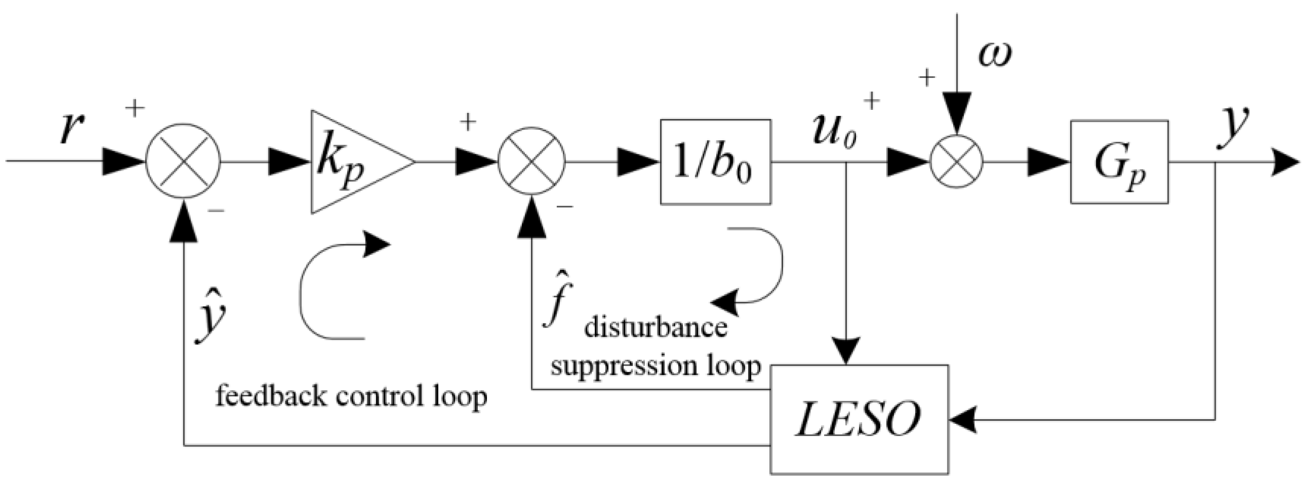
3.2. Linear Active Disturbance Rejection Control

LADRC consists of a linear extended state observer (LESO), and a linear state error feedback (LSEF) control law. LADRC is composed of disturbance suppression loop and feedback control loop. The structure is shown in Figure 3. The uncertain factors of the system are estimated in advance by the LESO and eliminated by the disturbance suppression loop, which is combined with the feedback control loop to improve the transient and stability performance of the system.
r is the input reference; u0 is the controlled quantity; ω is external disturbance of the system; Gp is the controlled object; y is the system output; y ^ is the estimated value of system output; f ^ is the estimated value of the total disturbance; kp is the controller parameter; and b0 is the system gain.
The first-order single-input single-output system is analyzed as follows:
y ˙ = b 0 u 0 + f ( y , u 0 )
where f is the total disturbance of the system.
Let x1 = y, x2 = f, then
{ x ˙ = A x + B u 0 + E f ˙ y 1 = C x
where A = [ 0 1 0 0 ] , B = [ b 0 0 ] , E = [ 0 1 ] , C = [ 1 0 ] , x = [ x 1 x 2 ] .
The corresponding continuous LESO is
{ x ^ ˙ = A x ^ + B u 0 + L 0 ( y y ^ ) y ^ = C x ^
where L o = [ β 1 β 2 ]
For first-order system, proportional control is adopted:
u = k p ( r x ^ 1 )
The total disturbance action is observed by the LESO as the expansion state of the system. To achieve automatic compensation of the total disturbance, the final control law is designed as
u 0 = u x ^ 2 b 0 = k p ( r x ^ 1 ) x ^ 2 b 0 = K p ( R ^ x ^ )
where R ^ = [ r 0 ] is the input reference and K p = [ k p 1 ] / b 0 is gain of controller.
Substitute Equation (12) into Equation (6) to get
y ˙ = x ^ 2 + u + f u
In summary, LADRC can be described as the form of state space as follows:
{ x ^ ˙ = ( A L o C ) x ^ + B u 0 + L o y u 0 = K p ( R ^ x ^ )
The gain Lo of the LESO and Kp of the LSEF are designed. By introducing the concept of bandwidth, the setting of Lo and Kp is converted into the observer’s bandwidth ωo and the controller’s bandwidth ωc, which simplifies the parameter tuning process.
The characteristic equation of LESO can be obtained from Equation (14)
| s I ( A L 0 C ) | = [ s + β 1 1 β 2 s ] = s ( s + β 1 ) + β 2 = s 2 + β 1 s + β 2
All poles of the observer are assigned to −ωo, then
s 2 + β 1 s + β 2 = ( s + ω o ) 2
where ωo is the bandwidth of observer.
The closed-loop characteristic equation of the feedback control system is as follows:
| s I ( A B K p ) | = [ s + k p 0 0 s ] = s ( s + k p )
All poles of the controller are assigned to −ωc, where ωc is the controller bandwidth.
Combining Equations (15) and (16), the equivalent equation are obtained as
β 1 = 2 ω o , β 2 = ω o 2 , k p = ω c

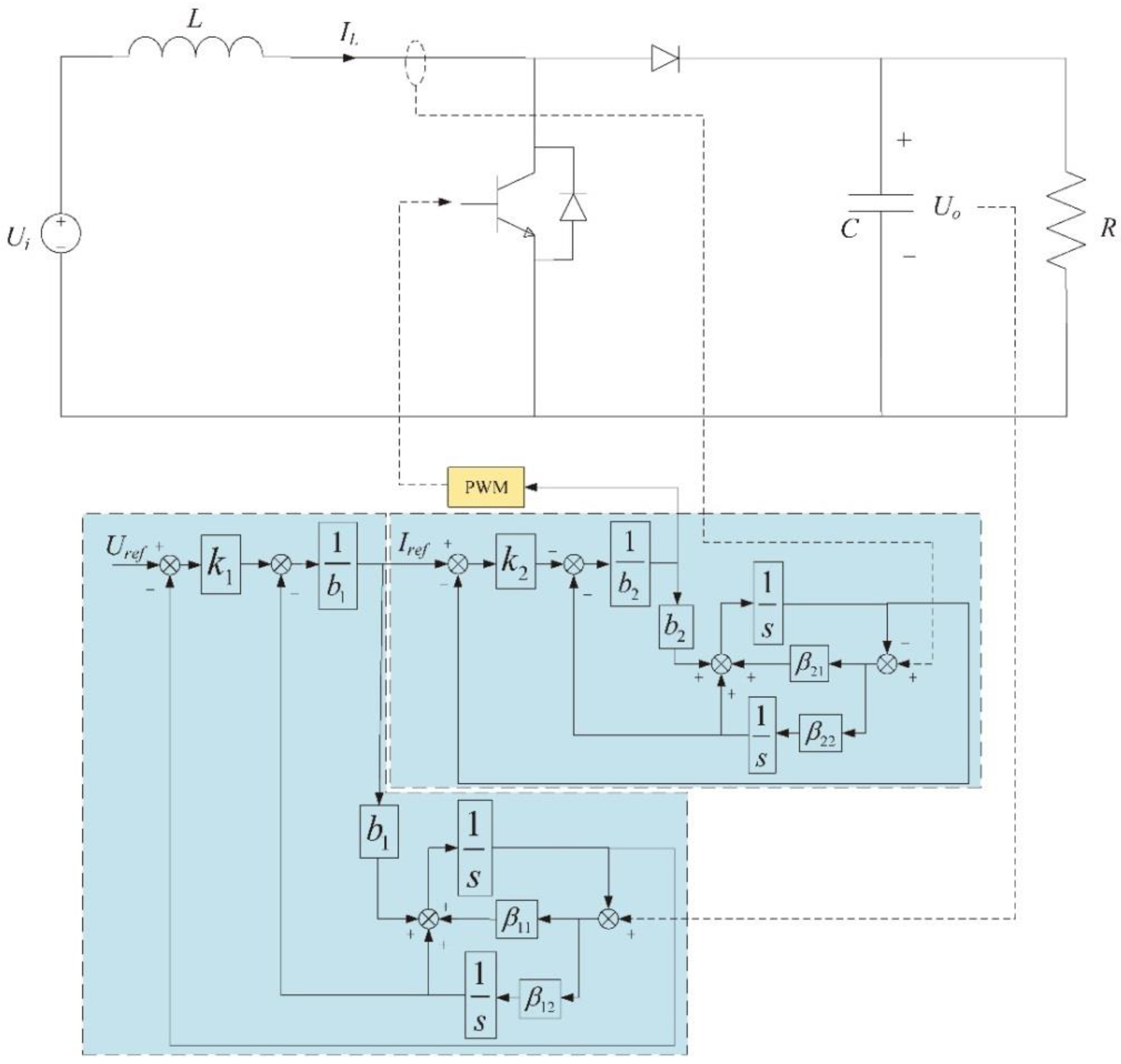
4. Controller Design

For the average model of the DC/DC boost converter established by Equation (3), this paper designs inner-loop current controller and outer-loop voltage controller based on LADRC. It has the characteristics of two-channel control with interference suppression and control feedback. LESO can be used to estimate the fluctuations of input voltage and loads in advance, which can be eliminated by disturbance suppression loop to improve the rapidity of the system. To avoid the problem of controlled quantity delay caused by error feedback from PI control, capacitive voltage signal and inductive current signal are, respectively, obtained by the LESO, which are used as the feedback quantity of voltage outer loop and current inner loop. Moreover, LESO has a filter function, which can suppress the noise in the system and reduce the low-pass filtering in the traditional cascade control.

4.1. Design of Current Controller

Design the current controller according to the first formula in Equation (4); the current controller is designed as follows:
d I L d t = ( 1 d ) U ° L + U i L
Let IL = y1, d = u1, then
y ˙ 1 = U o L u 1 + U i L U o L = b 1 u 1 + f 1 ( y 1 , u 1 )
where b 1 = U o L is the object gain, y1 is the system output, u1 is the system input, and f 1 = U i L U o L = U i U o L is the total disturbance of the system.
Let x1 = y1, x2 = f1, then
{ x ˙ = A 1 x + B 1 u 1 + E 1 f ˙ 1 y 1 = C 1 x
where A 1 = [ 0 1 0 0 ] , B 1 = [ b 1 0 ] , E 1 = [ 0 1 ] , C 1 = [ 1 0 ] , and x = [ x 1 x 2 ] .
Second-order LESO is
{ x ^ ˙ = A 1 x ^ + B 1 u 1 + L o 1 ( y 1 y ^ 1 ) y ^ 1 = C 1 x ^
where L o 1 = [ β 11 β 12 ] .
According to Equation (19), the relative of the current is first-order, and proportional control is used:
u = k 1 ( r 1 x ^ 1 )
According to the expansion state x ^ 2 = f ^ 1 given by the LESO. To achieve automatic compensation of the total disturbance, the final control law is designed as
u 1 = u x ^ 2 b 1 = k 1 ( r x ^ 1 ) x ^ 2 b 1 = K 1 ( R ^ 1 x ^ )
where R ^ 1 = [ r 1 0 ] is the input reference and K 1 = [ k 1 1 ] / b 1 is gain of controller.
Substituting Equation (24) into Equation (20),
y ˙ 1 = x ^ 2 + u 1 + f 1 u 1
The tuning of Lo1 and K1 is converted to the tuning of the observer bandwidth ωo1 and the controller bandwidth ωc1. All poles of the observer are configured to −ωo1, and all poles of the controller are configured to −ωc1.
β 11 = 2 ω o 1 , β 12 = ω o 1 2 , k 1 = ω c 1

4.2. Design of Voltage Controller

Design a voltage controller according to the second formula in Equation (4); the voltage controller is designed as follows:
d U o d t = ( 1 d ) I L C 1 R C U o
Let Uo = y2, IL = u2, then
y ˙ 2 = 1 d C u 2 y 1 R C = b 2 u 2 + f 2 ( y 2 , u 2 )
where b 2 = 1 d C is the object gain, y2 is the system output, u2 is the system input, and f 2 = y 2 R C is the total disturbance of the system.
Let x1 = y2, x2 = f2, then
{ x ˙ = A 2 x + B 2 u 2 + E 2 f ˙ 2 y 2 = C 2 x
where A 2 = [ 0 1 0 0 ] , B 2 = [ b 2 0 ] , E 2 = [ 0 1 ] , C 2 = [ 1 0 ] , x = [ x 1 x 2 ] .
Second-order LESO is
{ x ^ ˙ = A 2 x ^ + B 2 u 2 + L o 2 ( y 2 y ^ 2 ) y ^ 2 = C 2 x ^
where L o 2 = [ β 21 β 22 ] .
According to Equation (27), the dynamic characteristics of the voltage is first-order, so proportional control is used:
u = k 2 ( r 2 x ^ 1 )
To achieve automatic compensation of the total disturbance, the final control law is designed as
u 2 = u x ^ 2 b 2 = k 2 ( r x ^ 2 ) x ^ 2 b 2 = K 2 ( R ^ 2 x ^ )
where R ^ 2 = [ r 2 0 ] is the input reference and K 2 = [ k 2 1 ] / b 2 is the controller gain.
Substituting Equation (32) into Equation (28),
y ˙ 2 = x ^ 2 + u 2 + f 2 u 2
The Lo2 and K2 tuning is converted to the tuning of the observer bandwidth ωo2 and the controller bandwidth ωc2. All poles of the observer are configured to −ωo2, and all poles of the controller are configured to −ωc2.
β 21 = 2 ω o 2 , β 22 = ω o 2 2 , k 2 = ω c 2
Based on the above controller, the structure of the proposed controller is shown in Figure 4.

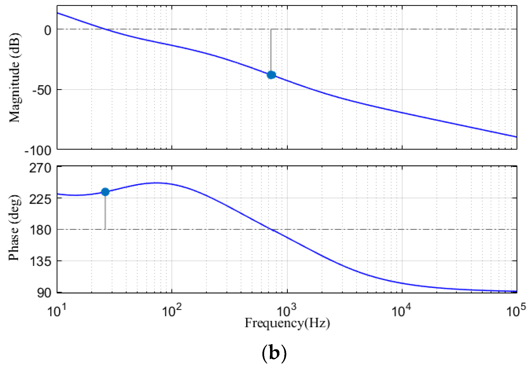
4.3. System Stability Analysis

The transfer function of the DC/DC boost converter can be obtained from Equation (4)
G p ( s ) = Δ U o ( s ) Δ d ( s ) = s L R I L + D R U o s 2 L C R + s L + D 2 R
where D = 1 − d and R is the load. As is shown in Equation (35), there is a zero in the right half plane. The bode diagram of Gp(s) is shown in Figure 5.
As can be seen in Figure 5, the phase margin of Gp(s) is −16.3 deg and the amplitude margin is −33.6 dB. According to the stability criterion of closed-loop control system, the system is unstable.
Figure 6 shows the control structure for one converter with the implementation of the LADRC method.
In Figure 6, Δ Uref is the reference voltage of the voltage loop, Δ Iref is the reference current of the current loop, and Δ Uo is the output voltage. The LADRC voltage outer loop is composed of H1(s) and Gc1(s), and the LADRC current inner loop is composed of H2(s) and Gc2(s). Gp1(s) is the transfer function of the controlled quantity to the output voltage, and Gp2(s) is the transfer function of the controlled quantity to the inductor current.
According to Equations (22), (23), (31) and (32), the transfer function of the first-order LADRC can be obtained as
H 1 ( s ) = k 1 s 2 + β 11 s + β 12 k 1 s 2 + ( k 1 β 11 + β 12 ) s + k 1 β 12
G c 1 ( s ) = 1 b 1 k 1 s 2 + ( k 1 β 11 + β 12 ) s + k 1 β 12 s 2 + β 11 s
H 2 ( s ) = k 2 s 2 + β 21 s + β 22 k 2 s 2 + ( k 2 β 21 + β 22 ) s + k 2 β 22
G c 2 ( s ) = 1 b 2 k 2 s 2 + ( k 2 β 21 + β 22 ) s + k 2 β 22 s 2 + β 21 s
The Gp1(s) and Gp2(s) transfer functions are obtained by the DC/DC boost circuit small signal model.
The transfer function of the controlled quantity Δ d to the output voltage Δ Uo is
G p 1 ( s ) = Δ U o ( s ) Δ d ( s ) = s L R I L + D R U o s 2 L C R + s L + D 2 R
The transfer function of the controlled quantity Δ d(t) to the output current Δ IL is
G p 2 ( s ) = Δ I L ( s ) Δ d ( s ) = s U o R C + D I L R + U o s 2 L C R + s L + D 2 R
From Figure 6, the transfer function of the inner loop current loop can be obtained as follows:
G 1 ( s ) = G c 2 ( s ) H 2 ( s ) 1 + G c 2 ( s ) G p 2 ( s )
The system open loop transfer function is
G 0 ( s ) = H 1 ( s ) G c 1 ( s ) H 2 ( s ) G c 2 ( s ) G p 2 ( s ) G p 1 ( s ) 1 + G c 2 ( s ) G p 2 ( s )
To verify the effectiveness of the proposed method, bode diagram is used to analysis the stability of the system. The current loop bode diagram is shown in Figure 7a, and the voltage loop bode diagram is shown in Figure 7b.
According to Figure 7a, the phase margin of current loop is 26 deg and the amplitude margin is infinite. As shown in Figure 7b, the phase margin of Gp(s) is 53.7 deg and the amplitude margin is 38 dB. According to the stability criterion of the closed-loop control system, the closed-loop control system satisfies the stability characteristic, and the stability margin of system is excellent.

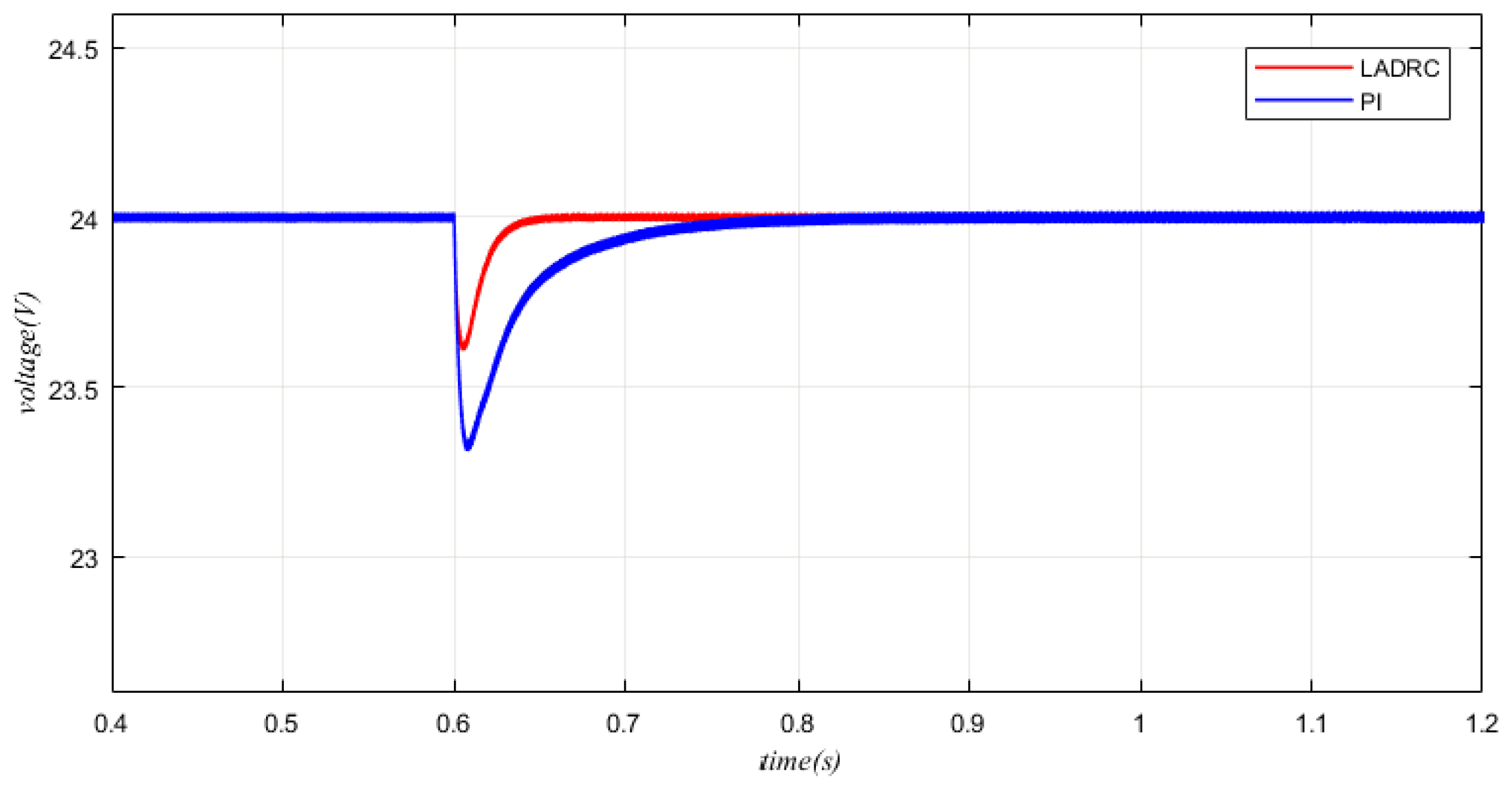
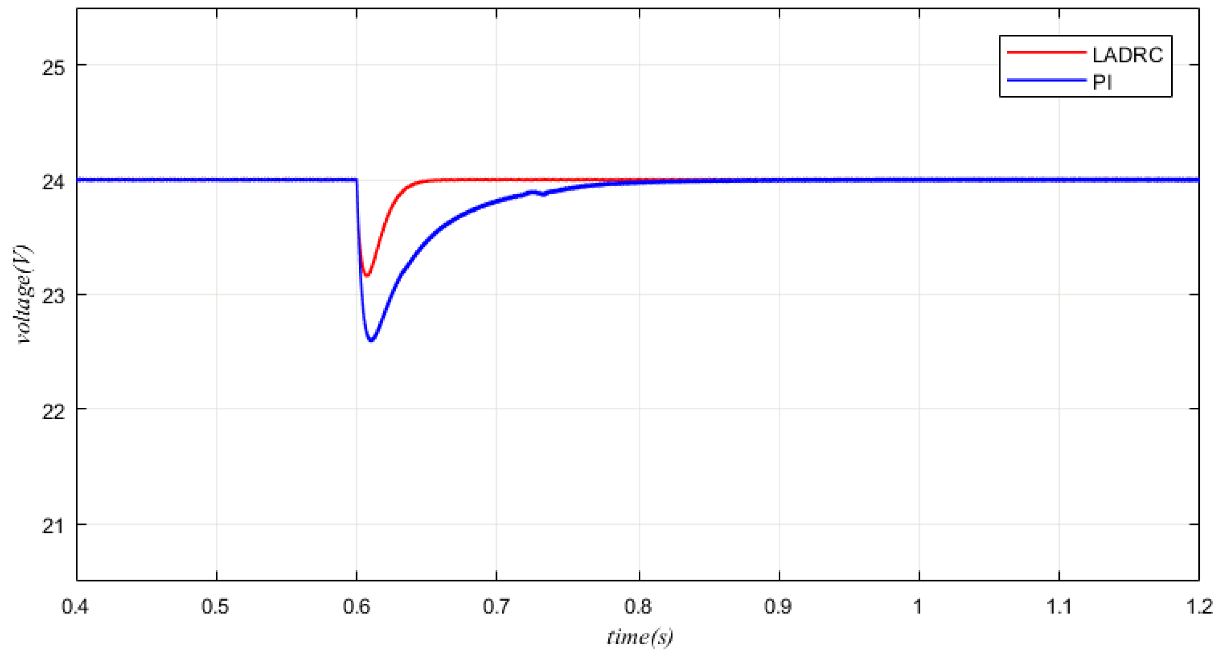
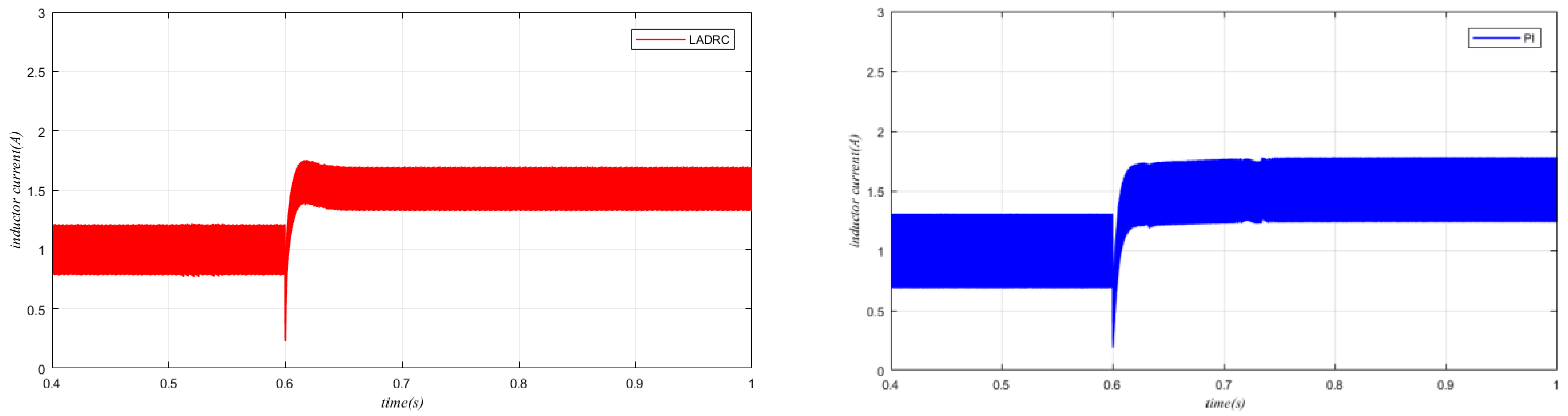
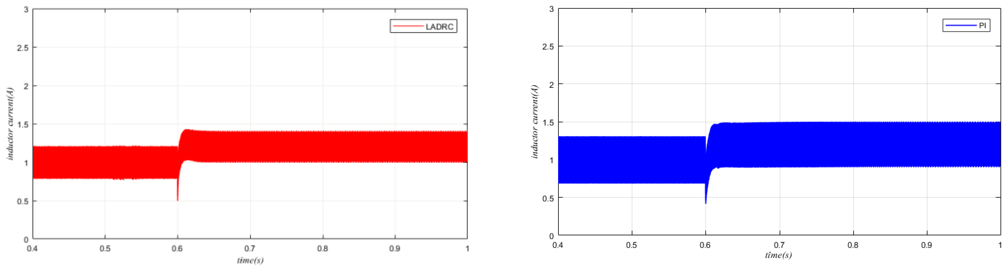
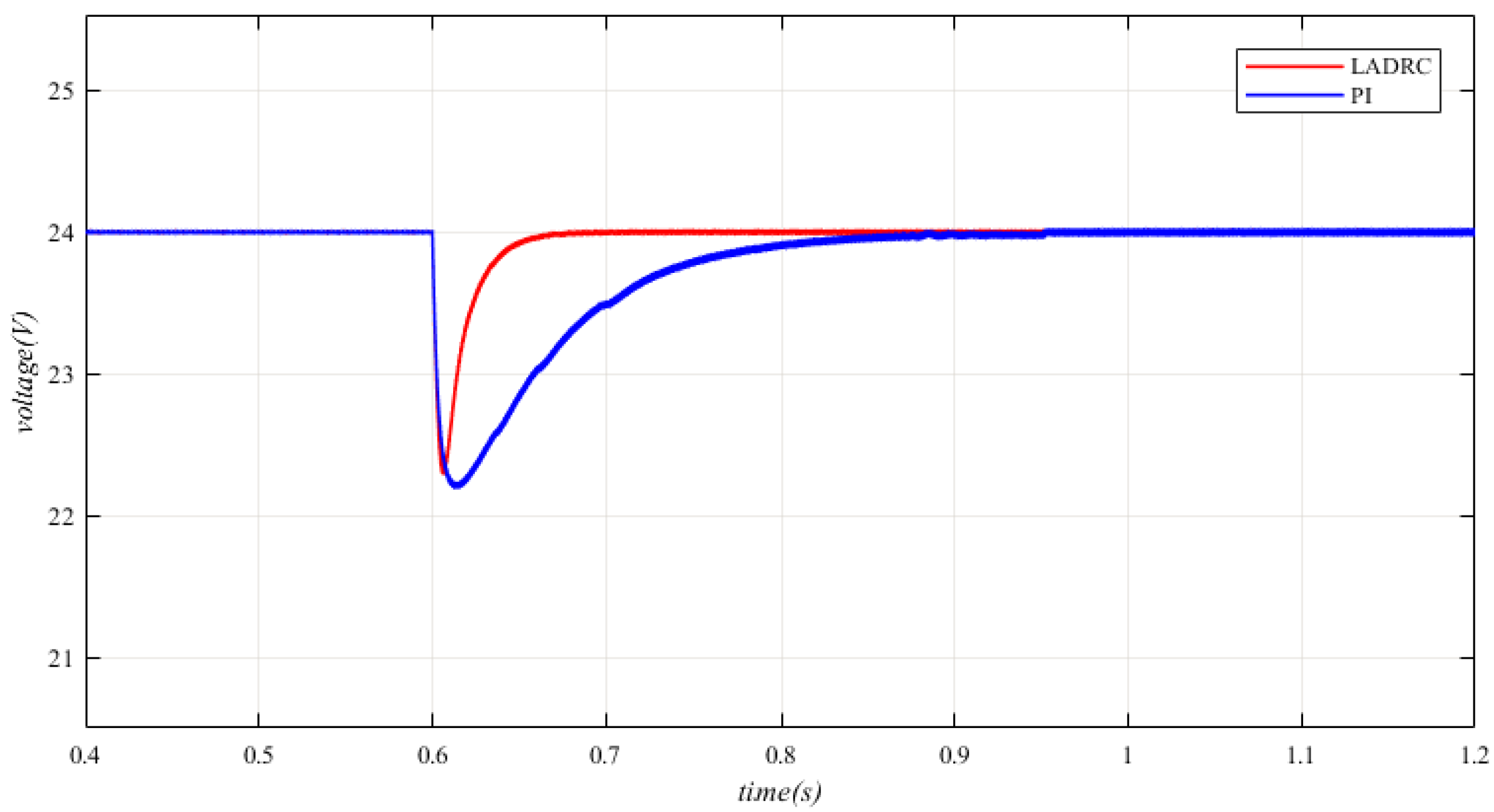
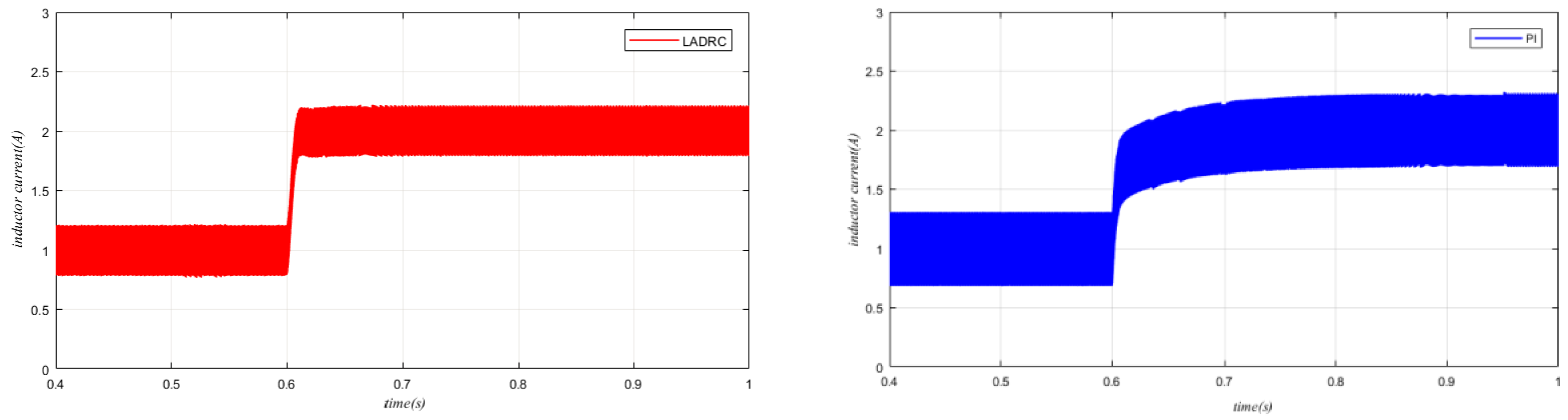
5. Simulation Results

To verify the performances of the proposed strategy, simulation tests were designed in Matlab/Simulink. Under the premise that PI cascade control and LADRC cascade control have no overshoot, the classical dual-loop PI controller was compared with the proposed controller to demonstrate the superiority of the proposed method. The circuit parameters and controller parameters in the simulation are shown in Table 1. To verify the stability of the system under different cases, three cases were designed, as shown in Table 2. For clarity, we will describe the variables and acronyms in the Appendix A.
Case 1: The converter input voltage was changed to examine the stabilization performance. At the beginning, the output voltage was regulated at 24 V with a 50 Ω resistance load. At 0.6 s, the input voltage of the converter was reduced from 12 V to 10 V. The voltage response is shown in Figure 8; the converter is controlled by LADRC cascade, the output voltage drops from 24 V at 23.6 V and reaches the desired value after 0.05 s. In contrast, the converter is controlled by PI cascade, the output voltage drops from 24 V to 23.3 V, and it takes 0.25 s to reach the desired value. The converter controlled by the proposed method can respond immediately and achieve the desired effect. At the same time, a longer response time and a large voltage deviation can be observed under the PI controller. The current response is shown in Figure 9; by further observing the change of the inductor current, both the LADRC control and the PI control can quickly reach the desired value, but the current shock of the PI control is larger than proposed method.
Case 2: To further validate the proposed control method, the changes of the input voltage were doubled. The basic setting was identical with the Case 1. Firstly, the output voltage was regulated at 24 V, and a 50 Ω resistance was connected to the DC bus. At 0.6 s, the input voltage of the converter was reduced from 12 V to 8 V. The output voltage response is shown in Figure 10; the converter is controlled by LADRC cascade, the output voltage drops from 24 V at 23.2 V and reaches the desired value after 0.07 s. In contrast, the converter is controlled by PI cascade, the output voltage drops from 24 V to 22.6 V, and it takes 0.28 s to reach the desired value. The current response is shown in Figure 11; the verification results are consistent with the results of Case 1.
Case 3: For load changes, the proposed control method was verified by Case 3. Initially, the output voltage was stable at 24 V and a 50 Ω resistance is connected. Then, the resistance decreased to 25 Ω in 0.6 s. The output voltage response is shown in Figure 12. With the same load change, the voltage deviation of PI control is 2.6 V and the recovery process is 0.35 s. The recovery process of the proposed control algorithm is 0.1 s, which is shorter than the recovery process of PI control by 0.25 s. Simulation results show that the proposed control algorithm has good dynamic performance. In addition, the output current response is shown in Figure 13; by observing changes of the inductor current, LADRC control can quickly reach the desired value, while PI control takes a long time to reach the desired value.

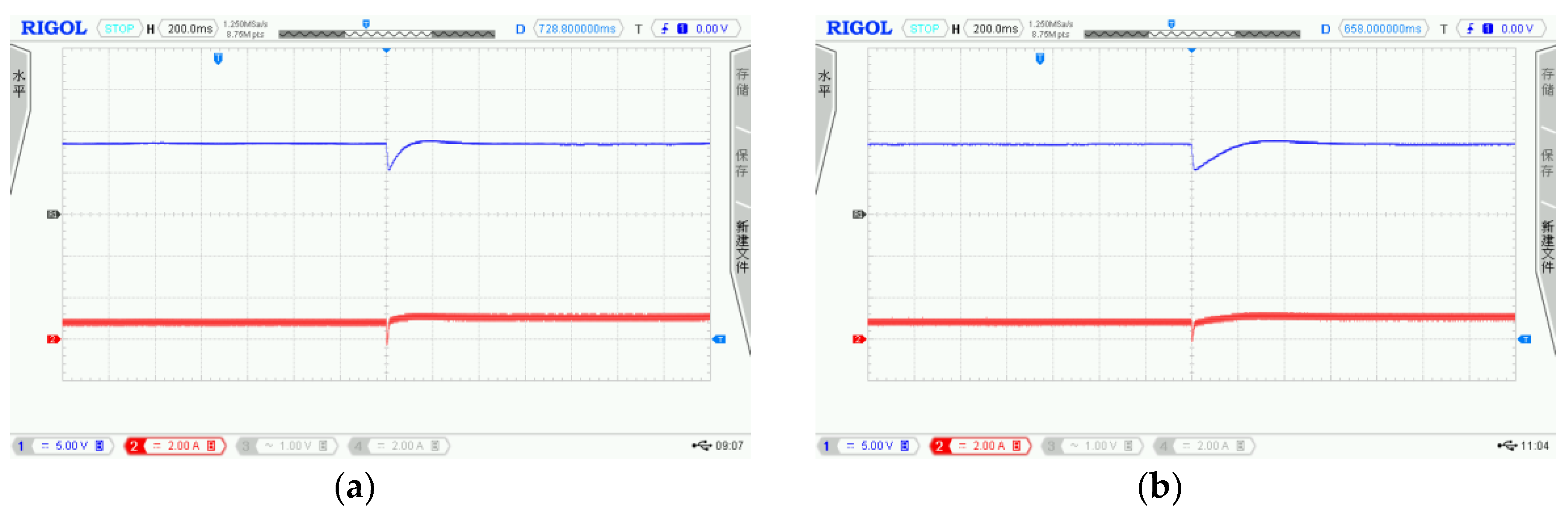
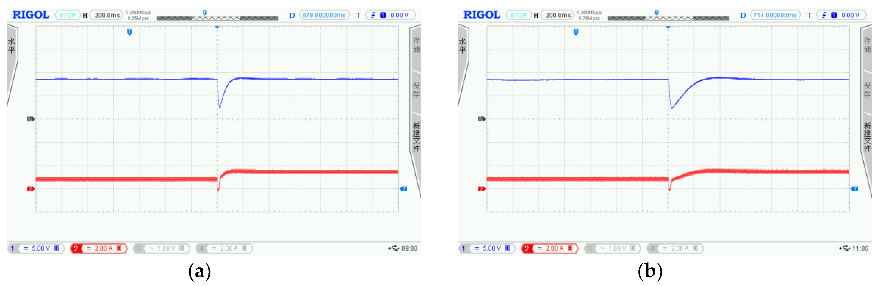
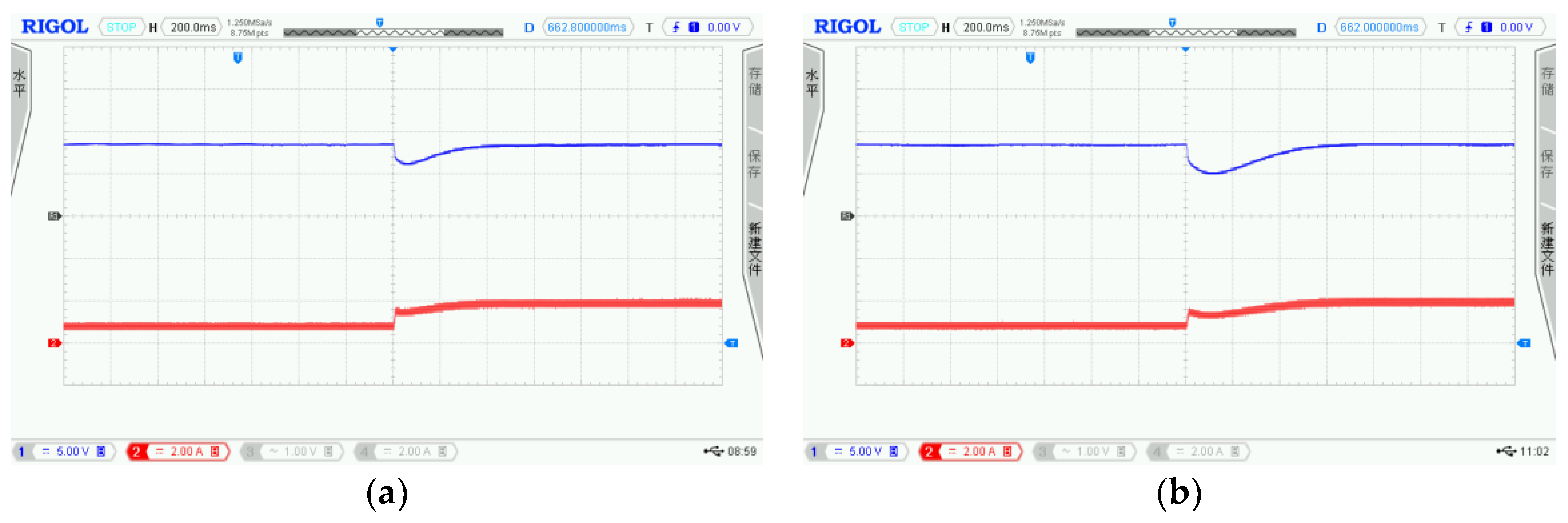
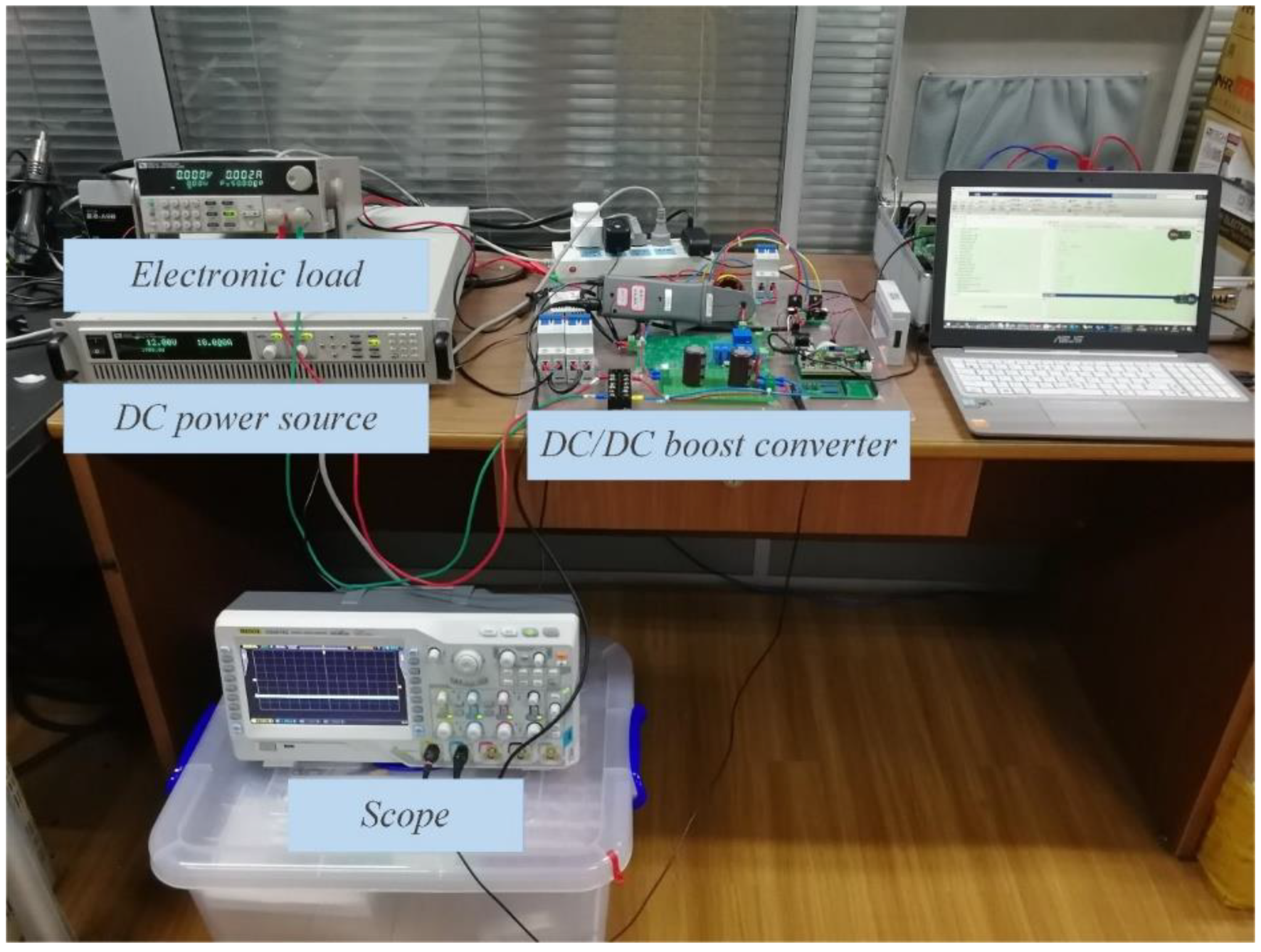
6. Hardware Experiment

To verify the proposed control method, a DC/DC boost converter experimental platform was built, as shown in Figure 14. The platform consists of a DC power source, a DC/DC boost converter, an electronic load, and a scope. Among them, the electronic load was set to the constant resistance mode. The circuit parameters are the same as those in the simulation, as shown in Table 1. To obtain the optimal actual control performance, ωc1, ωo1, ωc2, ωo2, kp1, ki1, kp2 and ki2 were redesigned as 33, 160, 300, 900, 0.03, 1, 0.05 and 2.
First, the input voltage of the boost converter was changed to examine the stability of the system. The output voltage was controlled at 24 V and a 50 Ω resistive load was connected to the voltage output. As shown in Figure 15, the input voltage of the boost converter drops from 12 V to 10 V. To ensure a constant output voltage, the current amplitude rises from 0.8 A to 1 A in a short time. The recovery time of the output voltage controlled by LADRC is shorter than the recovery time of the PI control. To further verify the stability of the system, the comparison of similar conditions continued, and the input voltage was changed by twice as much. Consistent with the previous results, the LADRC controller can bring the output voltage to the desired value faster. Experimental results are shown in Figure 16.
Second, the input voltage was set to 12 V and the load resistance was changed from 50 Ω to 25 Ω to verify the stability of the system under different loads. To ensure a constant output voltage, the current amplitude rises from 0.8 A to 2 A over a certain period. The experimental results are shown in Figure 17. The output voltage and inductor current controlled by LADRC reach the desired value more quickly than the PI control.

7. Discussion

To improve the control performance of DC/DC boost converter, this paper proposes a cascade control based on LADRC. To achieve the effect of eliminating unstable zero dynamics, the inductance current of the current loop is taken as a new output. Then, the indirect control is performed by the relationship between the inductance current and the output voltage to solve the non-minimum phase problem of DC/DC boost converter system. The instability of the output voltage caused by the fluctuation of input voltage and that of loads is solved by designing the LADRC controller. The simulation and experimental results show that the output voltage by using LADRC cascade control not only has good dynamic performance and steady state performance, but also has strong robustness under circumstances of the variation of input voltage and loads.

Author Contributions

Methodology, H.L. and X.L.; validation, X.L. and H.L.; writing—original draft preparation, X.L.; writing—review and editing, H.L. and X.L.; supervision, J.L. and H.L.; project administration, H.L. and J.L.; and funding acquisition, H.L. and J.L.

Funding

This research was supported by Shanghai International Science and Technology Cooperation Program (No.15220710500), Shanghai Science and Technology Commission Key Program (No.18DZ1203200), and 2019 Shanghai civil military integration development project (No. 2019-jmrh1-kj40).

Conflicts of Interest

The authors declare no conflict of interest.

Appendix A

SymbolsDescription
DCdirect current
ACalternating current
LADRClinear active disturbance rejection control
LSEFlinear state error feedback
LESOlinear extended state observer
ADRCactive disturbance rejection control
NLSEFnonlinear state error feedback
ESOextended state observer
TDtracking differentiator
PDproportional-derivative
PWMpulse width modulation
Uiinput voltage of DCDC boost converter
Uooutput voltage of DCDC boost converter
ILinductor current
Linductance value
Ccapacitance value
Rresistive load
fswswitching frequency
Tswitching period
dduty cycle
μ(t)pulse function
Uo(∞)the steady state values of Uo
IL(∞)the steady state values of IL
Uorefreference value of output voltage
ILrefreference value of inductor current
rfirst-order LADRC input reference
u0controlled quantity
ωexternal disturbance of the system
Gpcontrolled object
ysystem output
y ^ estimated value of system output
ftotal disturbance of the system
f ^ estimated value of the total disturbance
b0system gain
Kpgain of LSEF
Logain of LESO
ωoobserver’s bandwidth
ωccontroller’s bandwidth
D1-d
Gp(s)transfer function of the DC/DC boost converter
Δ Urefreference voltage of the voltage loop
Δ Irefreference current of the current loop
Δ Uooutput voltage
H1(s), Gc1(s)transfer function of LADRC voltage outer loop
H2(s), Gc2(s)transfer function of LADRC current inner loop
Gp1(s)transfer function of the Δ d to Δ Uo
Gp2(s)transfer function of the Δ d(t) to the Δ IL
G1(s)transfer function of the inner loop current loop
G0(s)system open loop transfer function
ωc1, ωo1, b1LADRC parameters of current control loop
ωc2, ωo2, b2LADRC parameters of voltage control loop
kp1, ki1PI parameters of voltage control loop
kp2, ki2PI parameters of current control loop

References

  1. Dragicevic, T.; Lu, X.; Vasquez, J.; Guerrero, J. DC Microgrids–Part I: A Review of Control Strategies and Stabilization Techniques. IEEE Trans. Power Electron. 2016, 31, 4876–4891. [Google Scholar] [CrossRef]
  2. El-Shahat, A.; Sumaiya, S. DC-Microgrid System Design, Control, and Analysis. Electronics 2019, 8, 124. [Google Scholar] [CrossRef]
  3. Baranwal, M.; Askarian, A.; Salapaka, S.; Salapaka, M. Distributed Architecture for Robust and Optimal Control of DC Microgrids. IEEE Trans. Ind. Electron. 2018. [Google Scholar] [CrossRef]
  4. Kakigano, H.; Nishino, A.; Ise, T. Distribution Voltage Control for DC Microgrids Using Fuzzy Control and Gain-Scheduling Technique. IEEE Trans. Power Electron. 2013, 28, 2246–2258. [Google Scholar] [CrossRef]
  5. Shenai, K.; Shah, K. Smart DC micro-grid for efficient utilization of distributed renewable energy. In Proceedings of the Energytech, Cleveland, OH, USA, 25–26 May 2011. [Google Scholar]
  6. Dragicevic, T.; Vasquez, J.C.; Guerrero, J.M.; Skrlec, D. Advanced LVDC Electrical Power Architectures and Microgrids: A step toward a new generation of power distribution networks. IEEE Elect. Mag. 2014, 2, 54–65. [Google Scholar] [CrossRef]
  7. Boujelben, N.; Masmoudi, F.; Djemel, M.; Derbel, N. Design and comparison of quadratic boost and double cascade boost converters with boost converter. In Proceedings of the 14th International Multi-Conference on Systems, Signals Devices (SSD), Marrakech, Morocco, 28–31 March 2017; pp. 245–252. [Google Scholar]
  8. Jou, H.; Huang, J.; Wu, J.; Wu, K. Novel Isolated Multilevel DC–DC Power Converter. IEEE Trans. Power Electron. 2016, 31, 2690–2694. [Google Scholar] [CrossRef]
  9. Zhang, C.; Gao, Z.; Chen, T.; Yang, J. Isolated DC/DC converter with three-level high-frequency link and bidirectional power flow ability for electric vehicles. IET Power Electron. 2019, 12, 1742–1751. [Google Scholar] [CrossRef]
  10. Leyva-Ramos, J.; Ortiz-Lopez, M.G.; Diaz-Saldierna, L.H.; Morales-Saldana, J.A. Switching regulator using a quadratic boost converter for wide DC conversion ratios. Power Electron. IET 2009, 2, 605–613. [Google Scholar] [CrossRef]
  11. Wang, Y.; Qiu, Y.; Bian, Q.; Guan, Y.; Xu, D. A Single Switch Quadratic Boost High Step up DC-DC Converter. IEEE Trans. Ind. Electron. 2018, 66, 4387–4397. [Google Scholar] [CrossRef]
  12. Wu, G.; Ruan, X.; Ye, Z. Non-isolated High Step-up DC-DC Converters Adopting Switched-capacitor Cell. Ind. Electron. IEEE Trans. 2015, 62, 383–393. [Google Scholar] [CrossRef]
  13. Chen, F.; Cai, X.S. Design of feedback control laws for switching regulators based on the bilinear large signal model. Power Electron. IEEE Trans. 1989, 5, 236–240. [Google Scholar] [CrossRef]
  14. Zhang, C.; Wang, X.; Lin, P.; Liu, P.X.; Yan, Y.; Yang, J. Finite-Time Feedforward Decoupling and Precise Decentralized Control for DC Microgrids Towards Large-Signal Stability. IEEE Trans. Smart Grid 2019. [Google Scholar] [CrossRef]
  15. Lee, T.S. Input-output linearization and zero-dynamics control of three-phase AC/DC voltage-source converters. Power Electron. IEEE Trans. 2003, 18, 11–22. [Google Scholar]
  16. Viswanathan, K.; Oruganti, R.; Srinivasan, D. Dual mode control of tri-state boost converter for improved performance. In Proceedings of the IEEE Power Electronics Specialist Conference, Acapulco, Mexico, 15–19 June 2003. [Google Scholar]
  17. Sastry, J.; Ojo, O.; Wu, Z. High performance control of a boost AC-DC PWM rectifier-induction generator system. In Proceedings of the Industry Applications Conference, Hong Kong, China, 2–6 October 2005. [Google Scholar]
  18. Wei, X.; Tsang, K.M.; Chan, W.L. DC/DC Buck Converter Using Internal Model Control. Electr. Mach. Power Syst. 2009, 37, 320–330. [Google Scholar] [CrossRef]
  19. Shuai, D.; Xie, Y.; Wang, X. The Research of Input-Output Linearization and Stabilization Analysis of Internal Dynamics on the CCM Boost Converter. In Proceedings of the International Conference on Electrical Machines Systems, Wuhan, China, 17–20 October 2008. [Google Scholar]
  20. Sira-Ramírez, H.; Silva-Ortigoza, R. Control Design Techniques in Power Electronics Devices; Springer: London, UK, 2006; pp. 235–355. [Google Scholar]
  21. Han, J. From PID to Active Disturbance Rejection Control. IEEE Trans. Ind. Electron. 2009, 56, 900–906.22. [Google Scholar] [CrossRef]
  22. Han, J. The auto-disturbance-rejection controller (ADRC) and its application. Control Decis. 1998, 1, 19–23. [Google Scholar]
  23. Gao, Z. Scaling and bandwidth-parameterization based controller tuning. In Proceedings of the American Control Conference, Denver, CO, USA, 4–6 June 2003; pp. 4989–4996. [Google Scholar]
  24. Gao, Z. Active Disturbance Rejection Control: A paradigm shift in feedback control system design. In Proceedings of the American Control Conference, Minneapolis, MN, USA, 14–16 June 2006. [Google Scholar]
  25. Gang, T.; Gao, Z. Benchmark tests of Active Disturbance Rejection Control on an industrial motion control platform. In Proceedings of the 2009 American Control Conference, St. Louis, MO, USA, 10–12 June 2009; pp. 5552–5557. [Google Scholar]
  26. Huang, Y.; Xue, W.; Gao, Z.; Sira-Ramirez, H.; Sun, M. Active Disturbance Rejection Control: Methodology, Practice and Analysis. In Proceedings of the Control Conference, Hilton, Portland, 4–6 June 2014. [Google Scholar]
  27. Song, C.; Wei, C.; Yang, F.; Cui, N. High-Order Sliding Mode-Based Fixed-Time Active Disturbance Rejection Control for Quadrotor Attitude System. Electronics 2018, 7, 357. [Google Scholar] [CrossRef]
  28. Li, H.; Qu, Y. A Composite Strategy for Harmonic Compensation in Standalone Inverter Based on Linear Active Disturbance Rejection Control. Energies 2019, 12, 2618. [Google Scholar] [CrossRef]
  29. Zuo, Y.; Zhu, X.; Li, Q.; Chao, Z.; Yi, D.; Xiang, Z. Active Disturbance Rejection Controller for Speed Control of Electrical Drives Using Phase-locking Loop Observer. IEEE Trans. Ind. Electron. 2019, 66, 1748–1759. [Google Scholar] [CrossRef]
  30. Zheng, Q.; Dong, L.; Lee, D.H.; Gao, Z. Active disturbance rejection control for MEMS gyroscopes. In Proceedings of the American Control Conference, St. Louis, MO, USA, 10–12 June 2009. [Google Scholar]
  31. You, J.; Fan, W.; Yu, L.; Fu, B.; Liao, M. Disturbance Rejection Control Method of Double-Switch Buck-Boost Converter. Energies 2019, 12, 278. [Google Scholar] [CrossRef]
Figure 1. DC/DC boost converter circuit.
Electronics 08 01249 g001
Figure 2. Impulse waveform.
Electronics 08 01249 g002
Figure 3. Structure of first-order LADRC.
Electronics 08 01249 g003
Figure 4. The structure of proposed controller.
Electronics 08 01249 g004
Figure 5. Bode diagram of Gp(s).
Electronics 08 01249 g005
Figure 6. Control structure of boost DC/DC converter.
Electronics 08 01249 g006
Figure 7. (a) Current loop open loop transfer function; and (b) open-loop bode diagram of systems with Controller.
Electronics 08 01249 g007aElectronics 08 01249 g007b
Figure 8. Output voltage responses in Case 1.
Electronics 08 01249 g008
Figure 9. Inductance current responses in Case 1.
Electronics 08 01249 g009
Figure 10. Output voltage responses in Case 2.
Electronics 08 01249 g010
Figure 11. Inductance current responses in Case 2.
Electronics 08 01249 g011
Figure 12. Output voltage responses in Case 3.
Electronics 08 01249 g012
Figure 13. Inductance current responses in Case 3.
Electronics 08 01249 g013
Figure 14. DC/DC boost converter experimental platform.
Electronics 08 01249 g014
Figure 15. (a) LADRC controller: experimental comparison responses with Case 1; and (b) PI controller: experimental comparison responses with Case 1.
Electronics 08 01249 g015
Figure 16. (a) LADRC controller: experimental comparison responses with Case 2; and (b) PI controller: experimental comparison responses with case 2.
Electronics 08 01249 g016
Figure 17. (a) LADRC controller: experimental comparison responses with Case 3; and (b) PI controller: experimental comparison responses with Case 3.
Electronics 08 01249 g017
Table 1. Simulation parameters.
ParametersDescriptionValue
UorefReference value of output voltage24 V
Linductance value1 mH
Ccapacitance value920 μF
fswswitching frequency10 KHz
ωc1, ωo1,b1LADRC parameters of current control loop165, 270, 543.5
ωc2, ωo2,b2LADRC parameters of voltage control loop1600, 8800, 24,000
kp1, ki1PI parameters of voltage control loop0.3, 7
kp2, ki2PI parameters of current control loop0.25, 30
Table 2. Different cases.
CaseInput VoltageLoad
112 V→10 V50 Ω
212 V→8 V50 Ω
312 V50 Ω→25 Ω

