Article

Broadband High-Gain Antenna for Millimetre-Wave 60-GHz Band

by
Khaled Issa
1,*,
Habib Fathallah
1,2,
Muhammad A. Ashraf
1,
Hamsakutty Vettikalladi
3 and
Saleh Alshebeili
1,3
1
KACST-TIC in Radio Frequency and Photonics for the e-Society (RFTONICS), Electrical Engineering Department, King Saud University, Riyadh 11421, Saudi Arabia
2
Laboratory of physics of materials-Structures and properties, Computer Department, Faculty of Sciences of Bizerte, University of Carthage, Carthage 1054, Tunisia
3
Department of Electrical Engineering, King Saud University, Riyadh 11421, Saudi Arabia
*
Author to whom correspondence should be addressed.
Electronics 2019, 8(11), 1246; https://doi.org/10.3390/electronics8111246
Submission received: 18 September 2019 / Revised: 25 October 2019 / Accepted: 25 October 2019 / Published: 31 October 2019
(This article belongs to the Section Microwave and Wireless Communications)

Abstract

:
This paper focuses on the 60 GHz band, which is known to be very attractive for enabling next-generation abundant multi-Gbps wireless connectivity in 5G communication. We propose a novel concept of a double-layer antenna, loosely inspired from standard log-periodic schemes but with an aperiodic geometry, reduced size, and a limited number of elements while achieving excellent performance over the entire 60 GHz band. To maximize the antenna’s efficiency, we have developed a design that differs from those traditionally used for millimeter-wave communication applications. We aim to simultaneously maximize the gain, efficiency, and bandwidth. The reflection coefficient of the proposed design achieves a bandwidth of 20.66% from 53.9 GHz up to 66.3 GHz, covering the entire frequency band of interest. In addition, this proposed structure achieves a maximum realized gain of 11.8 dBi with an estimated radiation efficiency of 91.2%. The proposed antenna is simulated, fabricated, and tested in an anechoic chamber environment. The measurement data show a reasonable agreement with the simulation results, with respect to the bandwidth, gain, and side-lobe level over the operational spectrum.

1. Introduction

The demand for high-speed radio links in 5G communication, ensuring high-data-rate wireless connectivity, is growing very fast. It is anticipated that in order to satisfy the consumer demands of higher data rates required in several modern multimedia applications, emerging millimeter-wave (MMW) smart technologies/devices can offer the solution with reduced cost, complexity, and power consumption. In this archetype, new standards, namely the IEEE 802.11ad [1] and IEEE 802.15.3c [2], have been presented for 60 GHz MMW-band wireless communications. Antenna elements with exceptional characteristics that exhibit higher gain, good efficiency, and the least dispersion to wideband input signals are desired to compensate for the losses and the impairments due to the propagation (both inside the devices and the free space) at higher frequency (60 GHz) bands. In fact, to ensure a high-quality, high-speed wireless connectivity, radio links highly rely on frontend performance, especially the performance of antenna elements. Therefore, for such high-frequency wireless frontends (including transmitter and receiver sides), antenna elements with features including compact size, low cost, and compatibility/integrability with other onboard MMW circuits are desirable. In such a paradigm, a printed antenna based on microstrip technology is a suitable alternative for satisfying the desired requirements. However, conventionally, microstrip antennas designed at the MMW bands typically exhibit low gain, low efficiency due to substrates’ losses, and narrow bandwidth [3]. Typically, for an emblematic wireless application, the desired physical and electrical specifications of the MMW antennas are achieved by carefully selecting an appropriate antenna terminology, with an advanced technology used for prototyping and realization by adopting suitable design approaches with modifications to the conventional antenna types [4]. Antenna arrays are usually used for high-gain frontend MMW wireless terminals [5]. However, such an approach is discouraged due to the considerable power losses and loss of compactness because of the mismatches among various circuit elements and the extended feeding network. In reference [6], an MMW antenna array operating at 60 GHz was designed and tested. The designed array of 16 × 16 elements exhibits a high gain of 30.5 dBi but with a low efficiency of around 40%. An antenna array of 10 elements operating at 60 GHz was presented that exhibits a maximum gain of 13 dBi with an efficiency of 63% [7]. In references [8] and [9], typical arrays of patch antenna elements were chosen to achieve high-gain. The realized gain cannot be higher than 19.6 dBi and 17.5 dBi using the 4 × 4 elements. However, both types of arrays operate over a wide bandwidth, which is around 27.5%. As an alternative, to enhance the bandwidth and the gain of microstrip-based antennas simultaneously, an aperture-coupled feeding approach has been suggested [9,10,11,12]. However, micromachining is required for the development of the multilayer circuits, which increases the complexity, cost, and vulnerability to the fabrication tolerances, especially for the antennas designed at MMW bands. In order to increase the bandwidth of microstrip antenna solely, multiple design approaches including various techniques such as loading of a slot inside the patch, introduction of thick dielectric material, broadband microstrip transitions, and slot coupling using multilayer technology were adopted. However, at 60 GHz MMW bands, these approaches are found least efficient in terms of achieving the desired electrical performance and bearing minor errors due to fabrication tolerances. Several other antennas based on low-temperature co-fired ceramic (LTCC) technology operating at 60 GHz frequency bands are demonstrated in the literature [13]. It can be inferred from their reported results that antenna arrays designed using LTCC technology can produce high-gain unit cells. However, performance enhancement is achieved by involving cutting-edge technology at a very high cost. Our key objective in this study is to outline a design procedure, based on the parametric analysis approach that can be used to enhance simultaneously the gain and the bandwidth of single antenna elements using conventional microstrip technology. In this paper, a modified log-periodic antenna, covering a broad spectrum of 12.4 GHz centered at the 60 GHz band, is proposed and demonstrated. The designed antenna exceeds the whole unlicensed 60 GHz bandwidth [57 GHz–66 GHz] [14], with a significant margin showing a flat gain greater than 10 dBi over the complete spectrum of interest. The maximum value of the gain is found to be 11.8 dBi at the center frequency of 60 GHz. Compared to the standard log-periodic antenna, our proposed concept has an aperiodic geometry, compact size, and a smaller number of elements. We investigate the effect of its geometric parameters and dimensions to maximize its performance, principally in terms of gain, bandwidth, and radiation characteristics. Multiple geometrical parameters are optimized by conducting parametric analysis while considering these desired specifications under the constraint of the lower fabrication accuracies. Our simulation results reveal that simultaneous improvements in the gain and in the bandwidth are mainly governed by varying the dimensions of different elements. The article is organized into five sections with Section 2 and Section 3 discussing the design geometry of the proposed antenna and the parametric analysis of its important geometric parameters. The measured performance of the realized antenna prototype is discussed in Section 4. Finally, the concluding remarks are summarized in Section 5.

2. Proposed Modified Log-Periodic Antenna

Our proposed antenna geometry was principally inspired by the log-periodic structure and to a lesser extent, towards the Yagi–Uda antenna principle. In the following subsections, we first provide a short overview of the principle of operation and the key concepts associated with both antennas and then introduce the general schematic of our proposed antenna that will be discussed in depth in the following sections.

2.1. Log-Periodic and Yagi–Uda Principles

The log-periodic dipole array (LPDA) is typically made of a series of dipoles or “radiating elements” positioned laterally to the antenna axis. By definition, the spacing between these elements obeys a logarithmic function. The different lengths of the elements led to different resonance frequencies, thus enabling a wide-bandwidth operation. This led to a series of ever-shorter dipoles towards the “longer side” of the antenna. The decreasing length of the elements made the LPDA look like a triangle or an arrow width resulting in the tip pointed towards the direction of the peak radiations. The Yagi–Uda antenna, on the other hand, controlled its performance parameters by adding elements of various lengths and spacings. However, the Yagi and the LPDA designs presented some important similarities because both were built based on at least one dipole element. The difference between the LPDA and Yagi became obvious when examining their electrical connections and the way the element lengths vary in the sequence. In summary, both LPDA and Yagi–Uda had a comparative edge over each other in terms of higher bandwidth and higher gain, respectively [15,16].

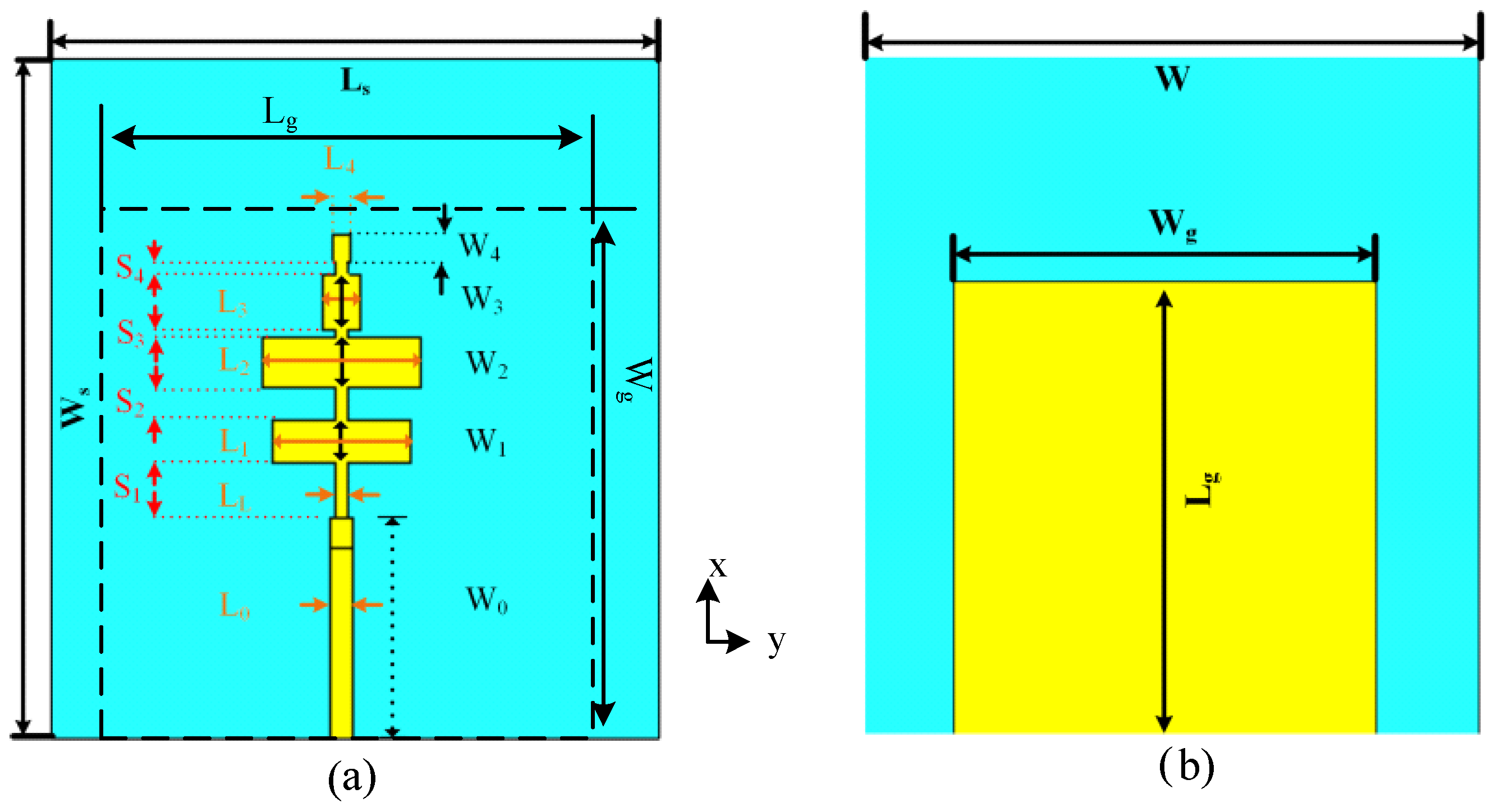
2.2. Description of the Proposed Antenna Concept

In our design, by optimizing element by element, we aimed to develop a hybrid antenna that can exhibit a larger bandwidth and a higher realized gain simultaneously. As shown in Figure 1, our proposed design was composed of 4 patches having variable lengths and spacing among each other. The presented design was clearly inspired by both the Yagi and LPDA concepts.
The antenna element was designed over a low-loss single layer dielectric substrate (Rogers Duroid RT5880) having a loss tangent of tanδ = 0.003 [17], dielectric constant of εr = 2.2, and thickness of h = 0.254 mm. The radiating elements were fed via a feed line having characteristic impedance of 50 Ω. Principally, a wideband antenna with a linear phase through the desired frequency range was recommended [18]
To obtain a linear phase-frequency characteristic, the feeding should be achieved from the longest dipole [19]. Hence, to achieve a linear phase response over the broadband, a simple microstrip feed line was more appropriate and more efficient. To initiate our design, we first determined the maximum length of the longest dipole Lmax. This obviously limits the maximum length that can be considered for all our elements [16,20]. This maximum was determined using:
l m a x = λ e f f m a x 4
where λeffmax is the maximum effective wavelength at the lowest resonant frequency. Once Lmax is known, the optimization of the other various geometric parameters of the structure starts. The length Ln and the width Wn of each element (number n) in the design can be progressively determined in relation to those of its previous neighbor element (number n-1), using the following simple equation,
L n L n 1 = W n W n 1 = τ   [ 16 ]
where τ is defined as the length to the width ratio (i.e., geometry constant). For each dipole element “n”, a spacing “Sn” is associated using the following equation
S n = 4 σ   L n   [ 16 ]
where σ is defined as the dipole spacing factor. In our design, the proposed antenna was aimed to operate over a larger bandwidth to maximize the throughput required for high-speed wireless communications. In Figure 1, we illustrated the general shape of our proposed antenna. It can be considered as a modified log-periodic antenna. The proposed antenna consisted of 4 elements, each of which had a different length and width in addition to the inter-element spacing. The initial set of parameters included the ground dimensions Lg and Wg. The second set of design parameters corresponded to the 4-cascaded elements. Each element (n = 1…4) was characterized by 3 parameters, namely length Ln, width Wn, and the spacing to its previous neighboring element Sn. In the rest of this paper, each set or subset of parameters will be optimized to obtain the best performance results in terms of maximum bandwidth and realized gain, minimum sidelobe and cross-polarization levels, and improved radiation pattern. During optimization and parametric analysis, full-wave electromagnetic simulation program CST Microwave Studio 2017 was used [21].

3. Simulation Results

In this section, we address the importance of each physical parameter of the proposed concept of designing a hybrid antenna. For simplicity of discussion, we did not report the simulation results related to all the geometric parameter values tested during the parametric study. Instead, for each geometric parameter (e.g., segment length, width, or spacing) we reported the obtained performance of the optimum value, in addition to that of the two suboptimum values, one lower and one higher. During the quest of the optimum value for each segment’s dimensions, we started from the initial values, and these were derived using the equations introduced in the above section for the LPDA antenna.

3.1. Number of Radiating Sections

In the standard log-periodic antenna, as we increased the number of elements, the antenna performance improved in terms of the gain and bandwidth until reaching a certain maximum. In our design, because we have tolerated the change of all the geometric parameters, we have observed that the performance in terms of gain and bandwidth, in addition to the other performance measurements that reached their optimum values at four elements only. In contrast, we have determined that 20 elements were needed in the standard log-periodic antenna to approach the bandwidth and the gain that we obtained [22]. During parametric analysis, we found that every parameter of every element had its own significance. The length of each element, in addition to the distance between each pair of neighboring elements, was critical to optimize the structure. Note that the width of each element also had an important impact on the design performance but omitted to simplify the discussion and avoid redundancy in the analysis. It is worthy of mentioning that during our search of optimum values, we simultaneously considered the maximization of the gain, the decrease of the sidelobe levels, and the cross-polarization level for both the E and H planes.

3.2. Parametric Study of the Antenna Multisections

As shown in Figure 1, our design was composed of four sections where each of them was characterized using the three independent sets of parameters. The dimensions of these elements were chosen based on the LPDA theory, then optimized to reduce the size and to increase the performance. The first step was a manual parametric study. We started this process by optimizing the first section (microstrip patch antenna). Then, we added the second section. It was worthy of mentioning that while optimizing the dimensions of each section the other antennas’ parameters were kept constant at their optimum value. At that point, we used a built-in algorithm in CST to verify that the obtained values were the optimum ones. We adopted this strategy until we finalized the antenna optimization (four sections). In the presented work, we presented the effect of changing the dimension of elements on the performance. The use of four legs enabled us to increase, simultaneously, the realized gain and decreased the side-lobe level and the cross-polarization level for both the E and H planes on the other side. However, the values of these parameters depend closely on the values of length and the spacing between these legs. For this reason, we have optimized the parameters of each leg. In each case we kept the optimum partial ground plane.

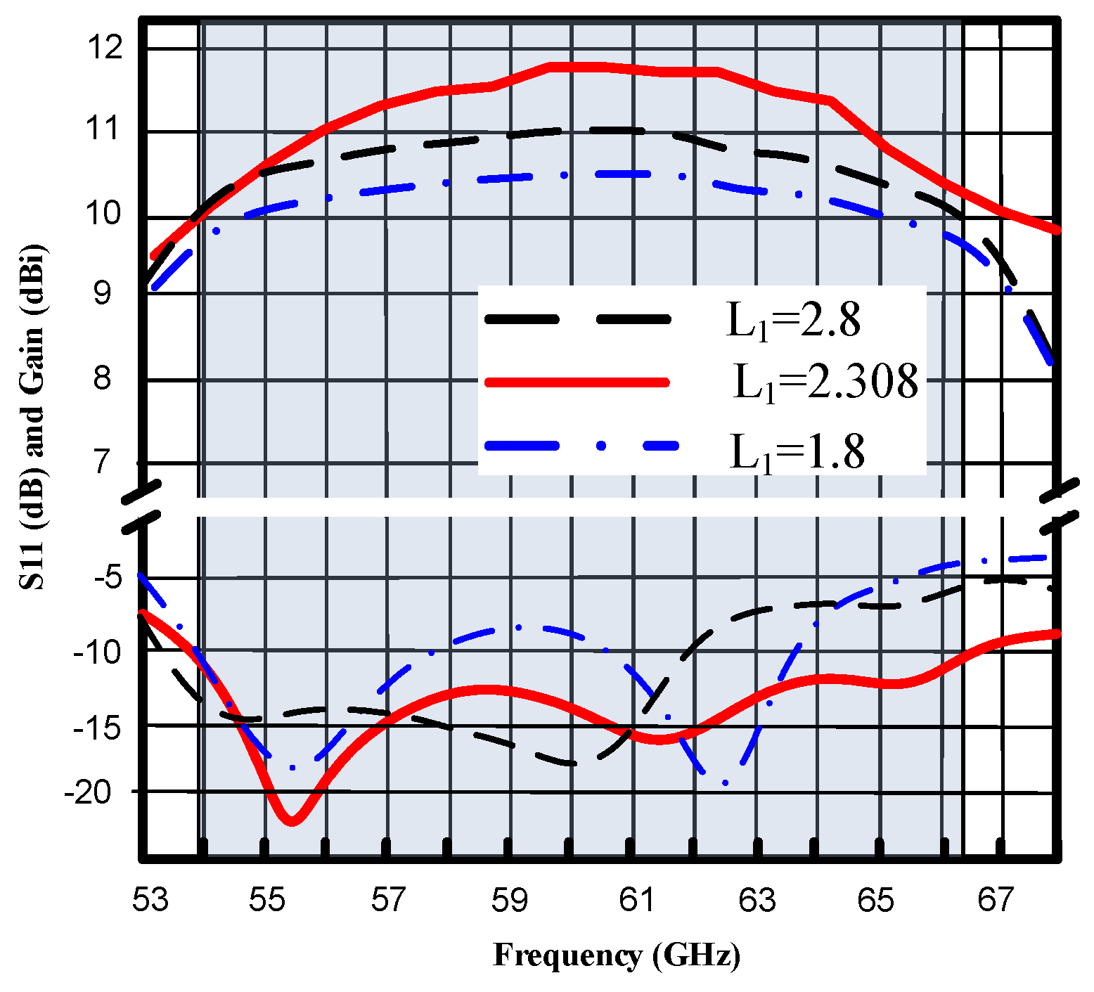
3.2.1. First Section Parametric Study

The optimization process has shown the critical importance of each geometric parameter in all four sections, affecting the performance characteristics of the proposed antenna. It is known that the gain of a Yagi antenna depends more on the length and spacing between elements than the elements’ number [21]. The antenna performance was not sensitive for W1 as much as L1, therefore we kept the optimum value of W1 as 2.3 mm. Figure 2 presents the effect of varying the first section’s length L1 on the reflection coefficient (S11) and the gain. It was noted that varying L1 had an influence on the S11 and gain performance, and it was found that the value of L1 =2.308 mm provided good bandwidth and stable high gain over the entire frequency of interest.

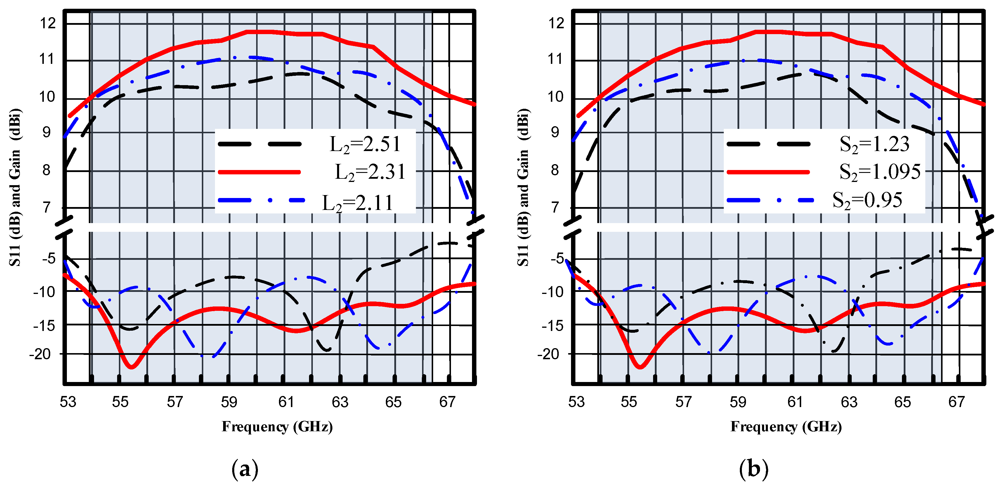
3.2.2. Second Section Parametric Study

For the second section, we found that the performance was incredibly sensitive to the length’s (L2) variations. Since the width W2 was not sensitive as much as L2, we kept the optimum value of W2 as 1.55 mm. As shown in Figure 3, by keeping the optimum value of L1 = 2.31 mm, for a small variation of 0.5 mm compared to the optimum value of L2 = 2.31 mm, we noticed a quick degradation of the reflection coefficient S11 and a decrease in the realized gain values. This observation can be explained by the fact that the length of an element strongly depends on the length of the previous leg L1. Also noted from Figure 3b that the spacing between the legs had a high influence on the antenna parameter, and the optimum value found was S2 = 1.095 mm. A small variation of the S2 value quickly affected the length to width ratio of each adjacent element, resulting in decreasing the antennas’ characteristics (bandwidth, gain, etc.), and this deterioration can reach up to 80% [22,23].

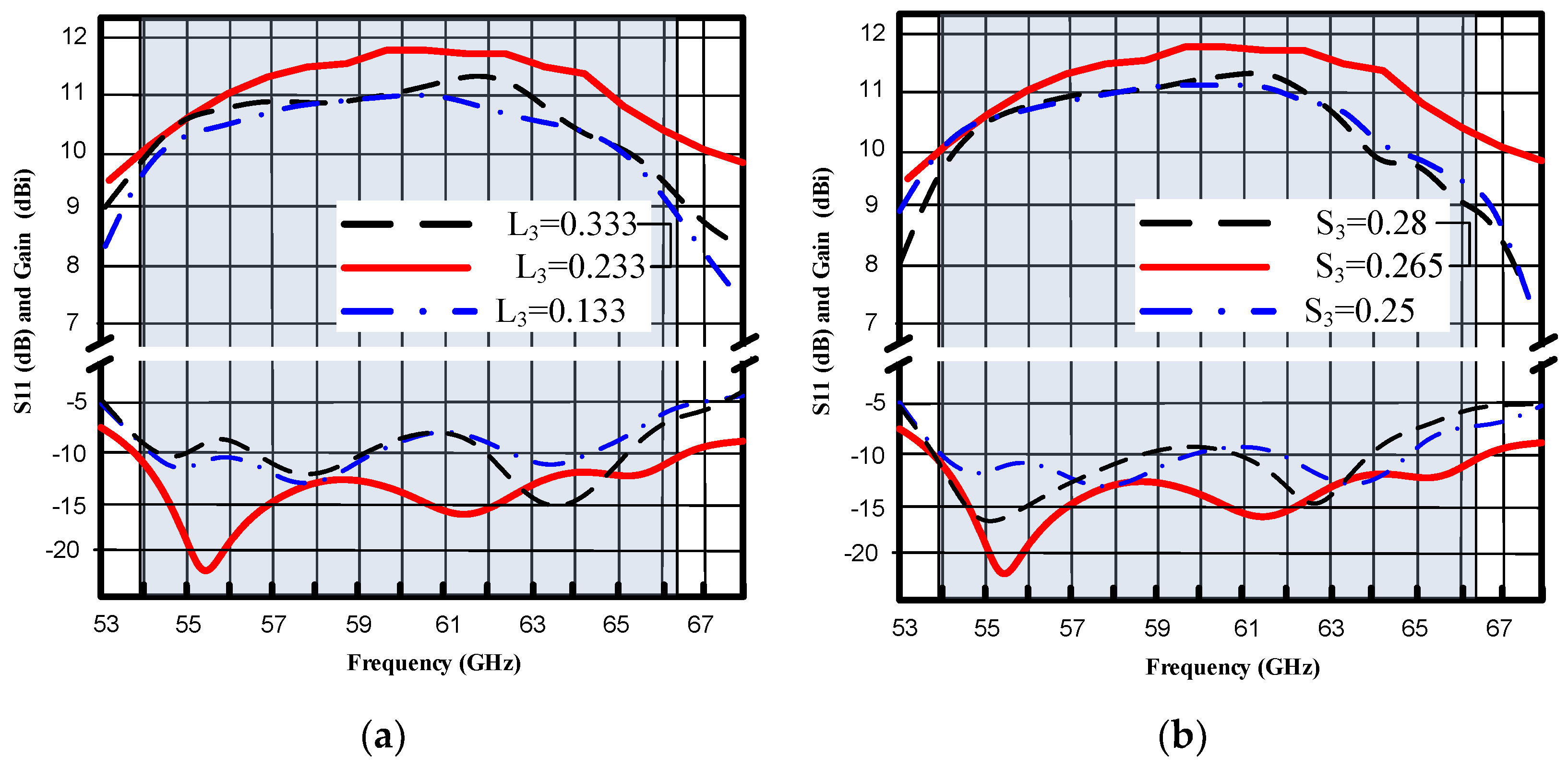
3.2.3. Third Section Parametric Study

The length (L3) and the spacing (S3) parameters for the third section were optimized to find suitable values satisfying the desired performance. Since the width W3 was not sensitive as much as L3, we kept the optimum value of W3 as 1.76 mm. As this section was joined with other sections, a very small variation in the length and spacing compared to all the previous ones strongly affected the antenna’s performance, as shown in Figure 4. Figure 4a shows the variation of L3 on antenna performance by keeping the optimum value of L1, L2, and S1. The best value of L3 was noted to be 0.233 mm. A small variation in the spacing S3 from 0.265 mm down to 0.25 mm decreased the bandwidth significantly from 12.4 GHz down to 6 GHz at 60 GHz, as seen in Figure 4b. The optimum value of S3 was found to be 0.265 mm.

3.2.4. Fourth Section Parametric Study

In Figure 5, the dependence of antenna performance on the length and the spacing of the fourth section is depicted. For all the previous geometric parameters, there was a direct dependency and impact on S11 and the gain. Based on the theoretical model described in reference [16,23], the mutual coupling between the different arms was a critical parameter to determine the response of the antennas. Indeed, the different lengths were responsible for the large or broad bandwidth; the spacings and the width affected the gain and the bandwidth. From Figure 5 the optimum values of L4 and S4 were found to be 0.61 mm and 0.6 mm, respectively.

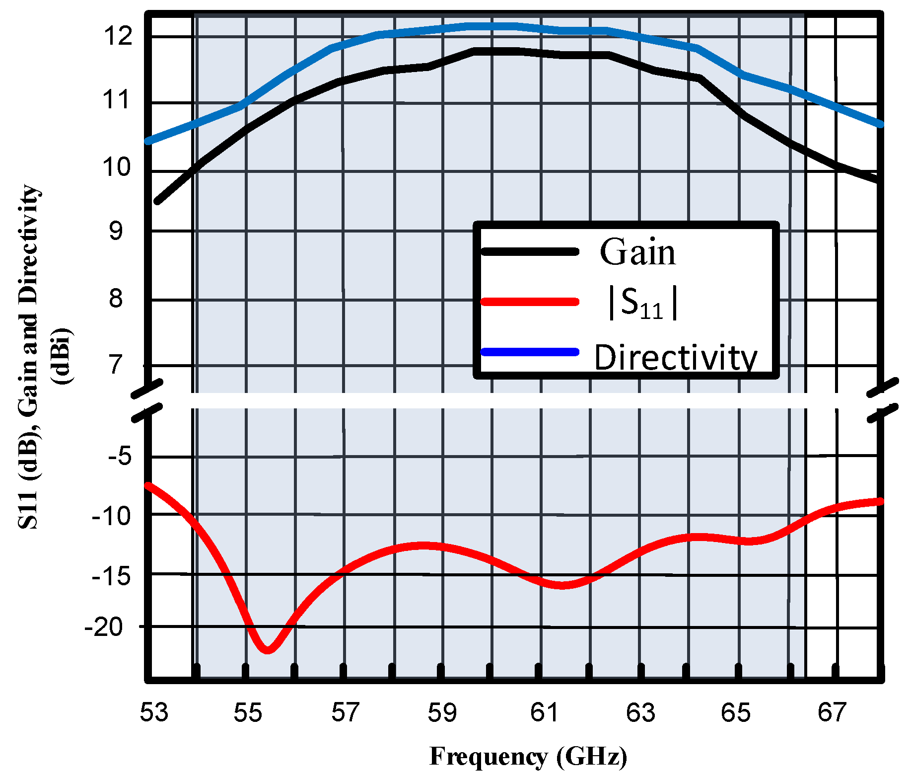
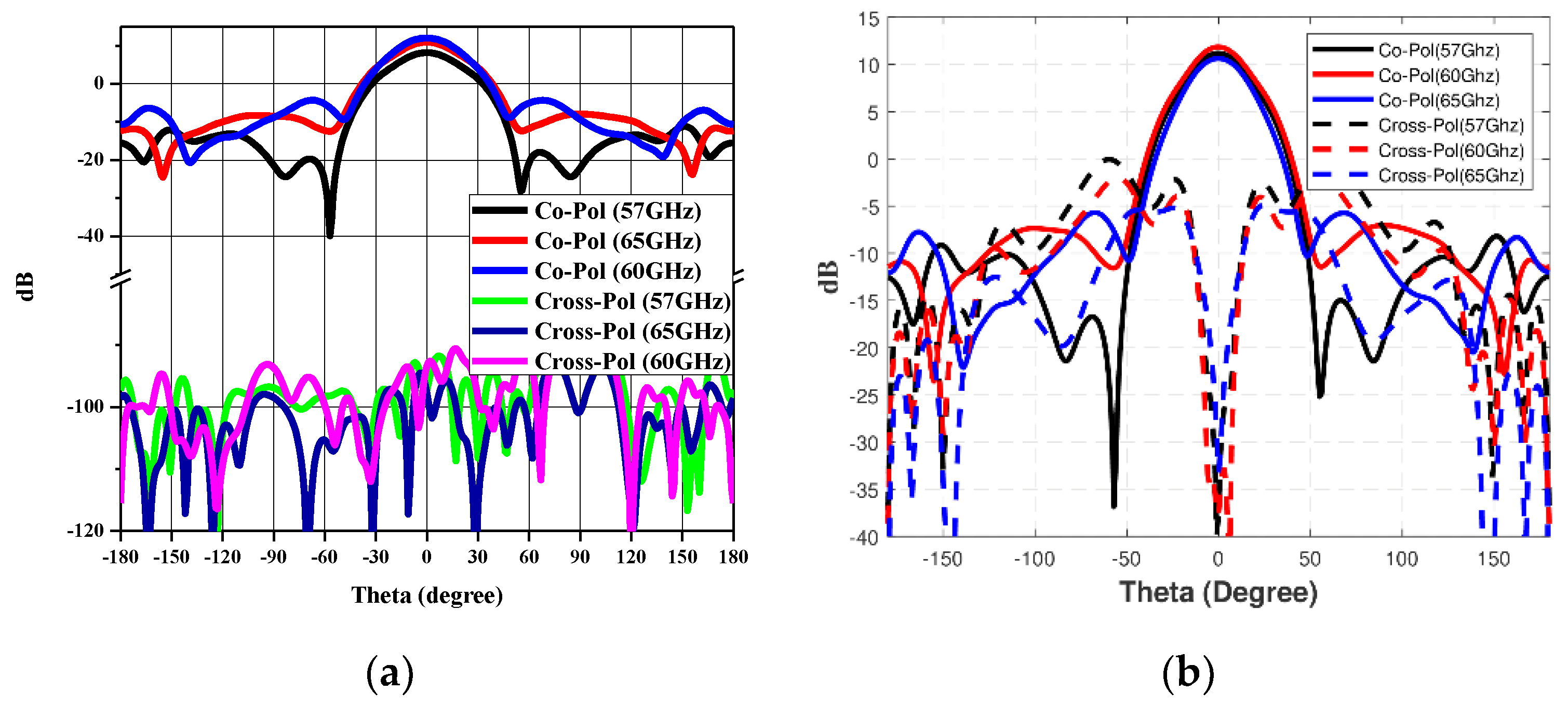
4. Optimal Design and Discussion

In the previous section, we showed the key steps in our design and examined the influence of each geometric parameter on the overall antenna performance. As the number of parameters was large, we only focused on the critical parameters that affected the antenna’s performance significantly. We optimized our proposed antenna to be used efficiently with broadband wireless terminals operating at the 60 GHz center frequency. In fact, one of the main goals of the step-by-step design process was to optimize the geometric parameters by varying the critical dimensions of the proposed hybrid structure to ensure simultaneously a sufficient value of the gain and a broad bandwidth.
The final optimized structure comprises four sections and a partial ground. The final optimized dimensions are reported in Table 1.
Figure 6 presents the simulation results of the final optimized structure. The figure encompasses the reflection coefficient S11 gain and directivity versus frequency from 53 up to 70 GHz. The simulated results show a bandwidth more than 12.4 GHz, from 53.9 up to 66.3 GHz. The antenna radiates at 60 GHz with a maximum gain of 11.8 dBi. In addition, the gain was found to be flat over the frequency band of interest from 57 to 64 GHz, and the realized gain was found to be more than 11.2 dBi. The efficiency was estimated to be 91.2% at 60 GHz. The designed high-gain antenna covering the broad bandwidth is suited for the next-generation 5G wireless applications proposed in the IEEE 802.11ad and IEEE 802.15.3c standards [1,2].
The normalized far-field intensity pattern for the E (θ varying from −180 to 180 degree and Φ = 0) and H (θ = 90 and Φ = varying from −180 to 180 degree) planes ((xz) and (yz) plane, respectively), versus the angle for 57, 60, and 65 GHz are depicted in Figure 7. The radiation pattern shows that the antenna was broadsided and linearly polarized. We observed that the E plane (xz) plane at 60 GHz had a half-power beamwidth of 45.10 degrees and a cross-polarization level of −11.4 dBi. The sidelobe level was less than −9 dB over the whole band of interest, and the minimum at 60 GHz was noted to be −11.4 dBi. For the H plane (yz) plane, the sidelobe level is found to be −14.5 at 60 GHz, and the cross-polarization level was −135.74 dB.
Table 2 reports the bandwidth and the gain in the 57–64 GHz range for various antenna types available in the literature that follow the same design approach presented in this work. It is clear that the proposed design outperforms the previously reported results, in terms of bandwidth and gain.

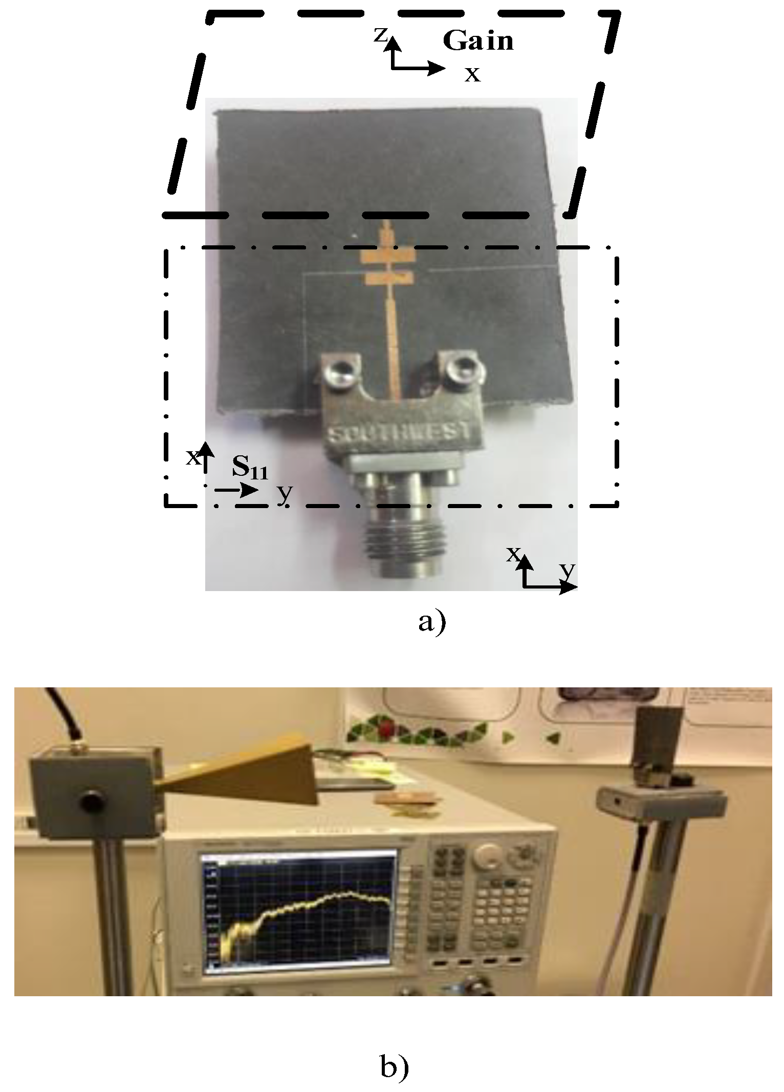
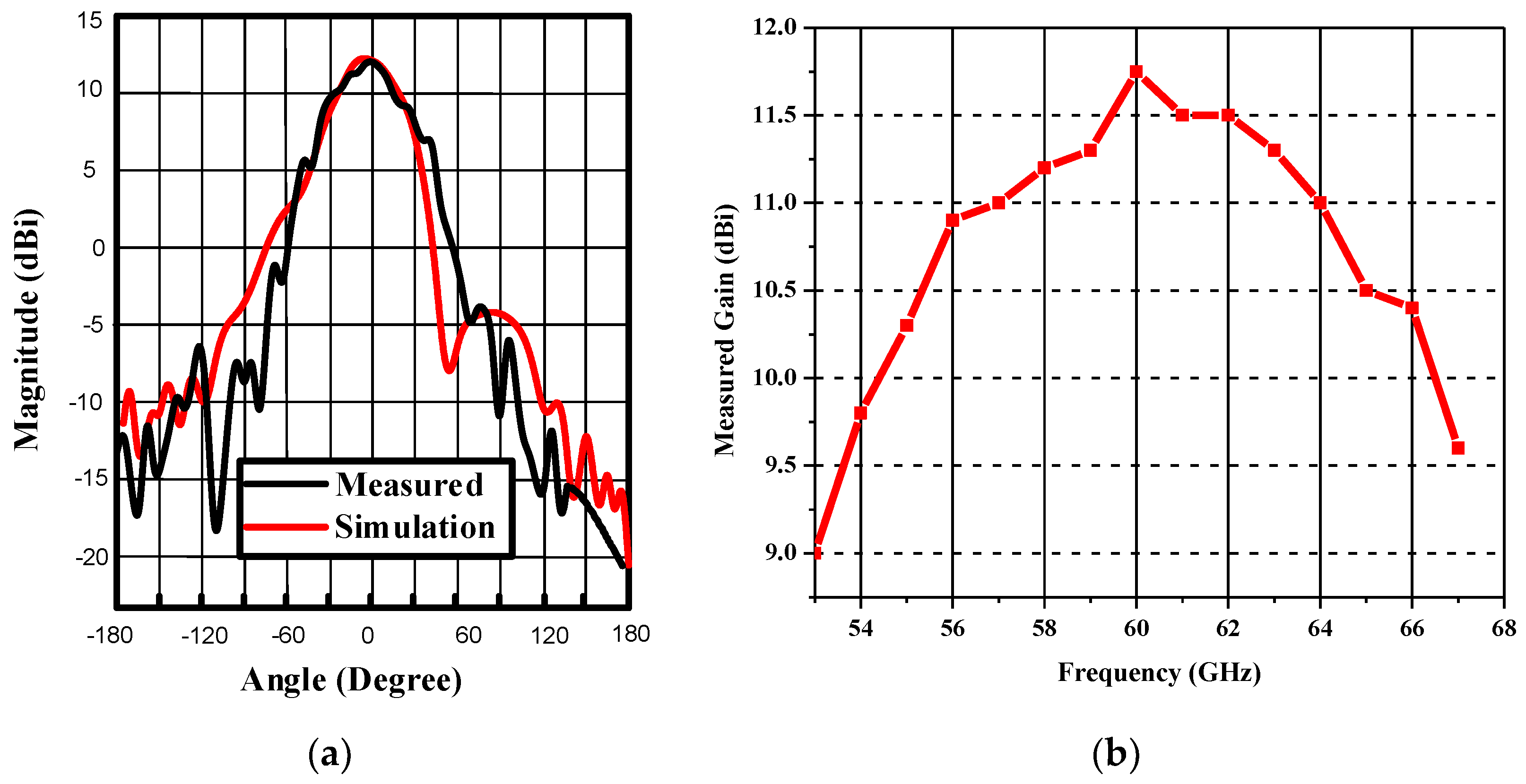
5. Experimental Results

The fabricated antenna’s S-parameters were measured using the Keysight vector network analyzer (PNAX; N5247A). To characterize the radiation pattern of the fabricated antenna prototype, we fixed the antenna in an in-house experimental measurement setup shown in Figure 8. The measurements were performed in a non-anechoic chamber laboratory environment. The transmit antenna and the antenna under test (AUT) were completely aligned using a laser alignment source. The transmitting and receiving antennas were placed with a separation distance that respects the far-field condition.
The measurement results, illustrated in Figure 9, show that the designed antenna matches well the simulation results in a wide frequency range, from 54 to 67 GHz, i.e., covering the entire desired spectral interval.
The measured and simulated antenna radiation pattern for the E plane at 60 GHz versus the angle is plotted in Figure 10. Based on these presented results, we notice that the simulation results and the measured results present a good agreement. The proposed modified periodic-log antenna achieves side-lobe suppression better than 11.26 dB in the E plane.

6. Conclusions

In this work, we proposed the concept of a double-layer antenna at 60 GHz. We aimed to simultaneously maximize the gain, efficiency, and bandwidth. The reflection coefficient S11 of the designed antenna was first simulated using the CST microwave studio, achieving a 12.4 GHz bandwidth. The proposed design is a vertically polarized antenna that is very appropriate for receiving/detecting function. The antenna achieved a maximum realized gain of 11.8 dBi with an efficiency of 91.2%. Our analysis of the geometric parameters demonstrated the importance of the number of dipoles clearly. Furthermore, the radiation pattern of E and H planes were presented. The simulation performance was in reasonable accordance with the measured performance. This work could be straightforwardly extended including more dipole elements to obtain more gain and bandwidth. The proposed antenna also finds application in V-band communication systems.

Author Contributions

Conceptualization, K.I. and H.F.; methodology, K.I., H.F. and H.V., and S.A.; software, K.I.; validation, K.I. and H.F.; formal analysis, K.I., H.F. and H.V.; investigation, K.I., H.F. and H.V.; resources, H.F., H.V and S.A.; data curation, K.I. and M.A.A.; writing—original draft preparation, K.I.; writing—review and editing, H.F., M.A.A., H.V. and S.A.; visualization, K.I. and M.A.A.; supervision, H.F. and S.A.

Funding

This research received no external funding.

Acknowledgments

This work was supported by King Saud University through the Researchers Supporting Project number (RSP-2019/46).

Conflicts of Interest

The authors declare no conflicts of interest.

References

  1. Nitsche, T.; Cordeiro, C.; Flores, A.B.; Knightly, E.W.; Perahia, E.; Widmer, J.C. IEEE 802.11 ad: Directional 60 GHz communication for multi-Gigabit-per-second Wi-Fi. IEEE Commun. Mag. 2014, 52, 132–141. [Google Scholar] [CrossRef]
  2. Scott-Hayward, S.; Garcia-Palacios, E. Multimedia resource allocation in mm-wave 5G networks. IEEE Commun. Mag. 2015, 53, 240–247. [Google Scholar] [CrossRef]
  3. Biglarbegian, B.; Fakharzadeh, M.; Busuioc, D.; Nezhad-Ahmadi, M.R.; Safavi-Naeini, S. Optimized microstrip antenna arrays for emerging millimeter-wave wireless applications. IEEE Trans. Antennas Propag. 2011, 59, 1742–1747. [Google Scholar] [CrossRef]
  4. Balanis, C.A. (Ed.) Modern Antenna Handbook; John Wiley and Sons: Hoboken, NJ, USA, 2011. [Google Scholar]
  5. Murugan, D.; Madhan, M.G.; Piramasubramanian, S. Design and performance prediction of 10GHz micro strip array antenna structures. In Proceedings of the 2012 Third International Conference on Computing, Communication and Networking Technologies (ICCCNT), Coimbatore, India, 26 July 2012; pp. 1–5. [Google Scholar]
  6. Liu, J.; Vosoogh, A.; Zaman, A.U.; Yang, J. Design and Fabrication of a High-Gain 60-GHz Cavity-Backed Slot Antenna Array Fed by Inverted Microstrip Gap Waveguide. IEEE Trans. Antennas Propag. 2017, 65, 2117–2122. [Google Scholar] [CrossRef]
  7. Karnfelt, C.; Hallbjorner, P.; Zirath, H.; Alping, A. High gain active microstrip antenna for 60-GHz WLAN/WPAN applications. IEEE Trans. Microw. Theory Tech. 2006, 54, 2593–2603. [Google Scholar] [CrossRef]
  8. Li, Y.; Luk, K.M. Low-cost high-gain and broadband substrate-integrated-waveguide-fed patch antenna array for 60-GHz band. IEEE Trans. Antennas Propag. 2014, 62, 5531–5538. [Google Scholar] [CrossRef]
  9. Wang, L.; Guo, Y.X.; Sheng, W.X. Wideband high-gain 60-GHz LTCC L-probe patch antenna array with a soft surface. IEEE Trans. Antennas Propag. 2013, 61, 1802–1809. [Google Scholar] [CrossRef]
  10. Rabbani, M.S.; Ghafouri-Shiraz, H. High gain microstrip antenna array for 60 GHz band point to point WLAN/WPAN communications. Microw. Opt. Technol. Lett. 2017, 59, 511–514. [Google Scholar] [CrossRef]
  11. Li, Y.; Luk, K.M. 60-GHz substrate integrated waveguide fed cavity-backed aperture-coupled microstrip patch antenna arrays. IEEE Trans. Antennas Propag. 2015, 63, 107–1085. [Google Scholar] [CrossRef]
  12. Zhang, T.; Li, L.; Xia, H.; Zhao, D.; Cu, T. Low-cost aperture coupled integrated 60 GHz phased array antenna in PCB process. In Proceedings of the 2016 IEEE International Symposium on Antennas and Propagation (APSURSI), Fajardo, Puerto Rico, 26 June–1 July 2016; pp. 439–440. [Google Scholar]
  13. Jin, H.; Che, W.; Chin, K.S.; Shen, G.; Yang, W.; Xue, Q. 60- GHz LTCC Differential-Fed Patch Antenna Array with High Gain by Using Soft-Surface Structures. IEEE Trans. Antennas Propag. 2017, 65, 206–216. [Google Scholar] [CrossRef]
  14. Jouanlanne, C.; Clemente, A.; Huchard, M.; Keignart, J.; Barbier, C.; Le Nadan, T.; Petit, L. Wideband linearly polarized transmitarray antenna for 60 GHz backhauling. IEEE Trans. Antennas Propag. 2017, 65, 1440–1445. [Google Scholar] [CrossRef]
  15. Cheema, H.M.; Shamim, A. The last barrier: On-chip antennas. IEEE Microwave Mag. 2013, 14, 79–91. [Google Scholar] [CrossRef]
  16. Campbell, C.; Traboulay, I.; Suthers, M.; Kneve, H. Design of a stripline log-periodic dipole antenna. IEEE Trans. Antennas Propag. 1977, 25, 718–721. [Google Scholar] [CrossRef]
  17. Vettikalladi, H.; Lafond, O.; Himdi, M. High-efficient and high-gain superstrate antenna for 60-GHz indoor communication. IEEE Antennas Wirel. Propag. Lett. 2009, 8, 1422–1425. [Google Scholar] [CrossRef]
  18. Nuthakki, V.R.; Dhamodharan, S. UWB Metamaterial-based miniaturized planar monopole antennas. AEU-Int. J. Electron. Commun. 2017, 82, 93–103. [Google Scholar] [CrossRef]
  19. Zhai, G.; Cheng, Y.; Yin, Q.; Chiu, L.; Zhu, S.; Gao, J. Super high gain substrate integrated clamped-mode printed log-periodic dipole array antenna. IEEE Trans. Antennas Propag. 2013, 61, 3009–3016. [Google Scholar] [CrossRef]
  20. Peixeiro, C. Design of log-periodic dipole antennas. IEE Proc. H (Microw. Antennas Propag.) 1988, 135, 98–102. [Google Scholar] [CrossRef]
  21. Logarithmic Periodic Dipole Antenna Calculator. Available online: https://www.changpuak.ch/electronics/lpda.php (accessed on 18 September 2019).
  22. Chen, C.; Cheng, D. Optimum element lengths for Yagi-Uda arrays. IEEE Trans. Antennas Propag. 1975, 23, 8–15. [Google Scholar] [CrossRef]
  23. Cheng, D.K. Gain optimization for Yagi-Uda arrays. IEEE Antennas Propag. Mag. 1991, 33, 42–46. [Google Scholar] [CrossRef]
  24. Rabbani, M.S.; Ghafouri-Shiraz, H. A dual band patch antenna designed with size improvement method for 60 GHz band duplexer applications. Microw. Opt. Technol. Lett. 2017, 59, 2867–2870. [Google Scholar] [CrossRef]
  25. Zhang, G.; Pu, S.; Xu, X.; Liu, Y.; Wang, C. Design of 60-GHz microstrip antenna array composed through circular contour feeding line. In Proceedings of the IEEE Asia-Pacific International Symposium on Electromagnetic Compatibility (APEMC), Shenzhen, China, 17–21 May 2016; Volume 1, pp. 1010–1013. [Google Scholar]
  26. Zhang, G.; Pu, S.; Liu, Z.R.; Liu, W.F. Design of 60 GHz microstrip antenna array composed through annular feeding line. In Proceedings of the 2016 IEEE International Symposium on Antennas and Propagation (APSURSI), Fajardo, Puerto Rico, 26 June–1 July 2016; pp. 1649–1650. [Google Scholar]
  27. Rabbani, M.S.; Ghafouri-Shiraz, H. Improvement of microstrip patch antenna gain and bandwidth at 60 GHz and X bands for wireless applications. IET Microw. Antennas Propag. 2016, 10, 1167–1173. [Google Scholar] [CrossRef] [Green Version]
  28. Kramer, O.; Djerafi, T.; Wu, K. Very small footprint 60 GHz stacked Yagi antenna array. IEEE Trans. Antennas Propag. 2011, 59, 3204–3210. [Google Scholar] [CrossRef]
  29. Chen, X.P.; Wu, K.; Han, L.; He, F. Low-cost high gain planar antenna array for 60-GHz band applications. IEEE Trans. Antennas Propag. 2010, 58, 2126–2129. [Google Scholar] [CrossRef]
Figure 1. Geometric parameters of the proposed antenna design. (a) Front view, and (b) back view.
Electronics 08 01246 g001
Figure 2. First element parametric study: Realized gain and reflection coefficient. S11 versus frequency for three different values of lengths L1.
Electronics 08 01246 g002
Figure 3. Second element parametric study: Realized gain and reflection coefficient S11 versus frequency (a) for three different values of lengths L2 and (b) spacing S2 by keeping L1 at the optimum value of 2.31 mm.
Electronics 08 01246 g003
Figure 4. Third element parametric study: Realized gain and reflection coefficient S11 versus frequency for three different values (a) of lengths L3 and (b) spacing S3.
Electronics 08 01246 g004
Figure 5. Fourth element parametric study: Realized gain and reflection coefficient S11 versus frequency for three different values (a) of lengths L4 and (b) spacing S4.
Electronics 08 01246 g005
Figure 6. The realized gain, directivity, and reflection coefficient S11 for the derived optimum design.
Electronics 08 01246 g006
Figure 7. 2D radiation patterns in (a) E-plane and (b) H plane.
Electronics 08 01246 g007
Figure 8. (a) Fabricated antenna. (b) Experimental setup for the antenna. The excitation is made using a horn antenna (in the left). The fabricated 60 GHz antenna (in the right) is fixed and connected to the vector network analyzer.
Electronics 08 01246 g008
Figure 9. The reflection coefficient of the designed antenna versus the frequency (measurement vs simulation).
Electronics 08 01246 g009
Figure 10. The antenna realized gain (a) versus angle at 60 GHz for the E plane (measurement vs simulation) (b) measured at the frequency range 53–68 GHz.
Electronics 08 01246 g010
Table 1. Optimized parameters of proposed Antenna in mm.
LGWGLSWSL1W1S1W2
2526.6230303.32.31.841.55
L2S2L3W3S3L4W4S4
2.311.0950.231.760.260.610.810.6
Table 2. Physical lengths and the corresponding resonance frequencies of the slot resonators.
Antenna TypeBandwidth (GHz)Gain at 60 GHz (dB)Gain at 57–64 GHz (dB)
Superstrate Antenna [17]6.8%129.8–14.6
Dual Band [24]4.35%9.3N.A
Circular contour feeding line [25]0.5%8.4−6.8 to 8.4 (58 to 62 GHz)
Linear feeding line [26]N.A11.56.5 to 12 (58 to 62 GHz)
Annular Feeding Line [27]1.8%9.5−4 to 10.8 (58 to 62 GHz)
Yagi (PCB) [28]10.5%18n.a
Planar Antenna Array [29]4.2%2220.4 to 17.6 (59–62)
Proposed work20.7%11.8>11.2

