1. Introduction
Wireless communication and sensing systems are continuously raising new demands not only on performance of components, but also on their miniaturization, integration with on-chip devices, environmental effects, and costs. Planar components are easy to fabricate, result in low-profile circuits, and are therefore cost-efficient [
1,
2,
3,
4]. The current design of planar circuits still, however, follows a conventional approach that relies on assemblage of basic building blocks, such as filters, hybrid couplers, and antennas. The design of each component is accomplished in a separate design step and typically relies on simple structures inspired from circuit and transmission line theories. Although this design methodology is beneficial for design reuse, it results in large circuit footprints and high insertion losses.
Filtering antennas are components designed to offer antennas with specified filtering responses to decrease interference with surrounding wireless systems [
5,
6,
7,
8,
9]. The design of filtering antennas is currently accomplished by following one of two approaches. The first is to use a separate filtering structure that precedes the antenna [
10]. This approach has the drawback of increasing both the insertion loss and the footprint of the whole circuit. The second approach uses parasitic elements inside/near the antenna structure [
5,
6,
9]. This approach is suitable for narrow band antennas, such as microstrip antennas; however, it typically requires a redesign of the antenna to account for the presence of the parasitic objects. Moreover, this latter strategy is typically time-consuming and may result in structures that are complex to fabricate [
5,
11]. In a recent work, Liu et al. [
6] proposed to suppress the out-of-band radiation of a filtering patch antenna by using dissipative resistors. The use of dissipative resistors has the advantage of decreasing the energy reflected back to the amplifier. However, the dissipated energy increases the risk of heating up the circuit.
In the literature, most of the previously published filtering antennas rely on structures inspired from circuit and transmission line theories. Following a different approach, this work uses topology optimization techniques to design planar differential-fed filtering antennas. Topology optimization techniques, initially proposed for structural optimization [
12,
13], have been employed to design various electromagnetic components, such as antennas, filters, and waveguide transitions [
14,
15,
16,
17,
18]. In topology optimization, each pixel (2D) or voxel (3D) inside the design domain is subject to design. Hence, topology optimization techniques are sometimes referred to as being parameter-free methods. Typically, these optimization techniques rely on sensitivity analysis and gradient-based optimization methods to seek designs (shapes) that satisfy the design objectives. Because of the vast degrees of freedom handled by these algorithms, they can reveal new conceptual designs. Moreover, recent designs obtained by these techniques have proven their ability not only to offer novel devices, but also to provide designs that satisfy manufacturing constraints [
18].
The main interest of the current work is to optimize the antenna of a positioning system that operates over the frequency band 6.0–8.5 GHz. One essential operational requirement for such system is to possess a stable coverage over a wide beamwidth. Moreover, this positioning system is intended for use in sites where other wireless communication systems operating at the 5.8 GHz WiFi frequency band could be sources of mutual interference. Therefore, we propose to design differential-fed planar antennas that combine requirements on a wide impedance bandwidth, a stable directivity, and a filtering of the out-of-band frequencies. We aim to exploit the vast degrees of freedom offered by topology optimization to design such antennas. We formulate the problem of the antenna design as a mathematical topology optimization problem, in which all design requirements are embedded a priori as objective functions or constraints. That is, using a very large space of feasible designs, the algorithm seeks structures that accomplish multiple objectives. Using manual design procedures, it can be very difficult to manage a large design space and multiple objectives. The choice of differential lines to feed the antennas makes them suitable for use with differential RF amplifiers [
1]. Moreover, this type of feeding typically results in very low cross-polarization levels [
19,
20].
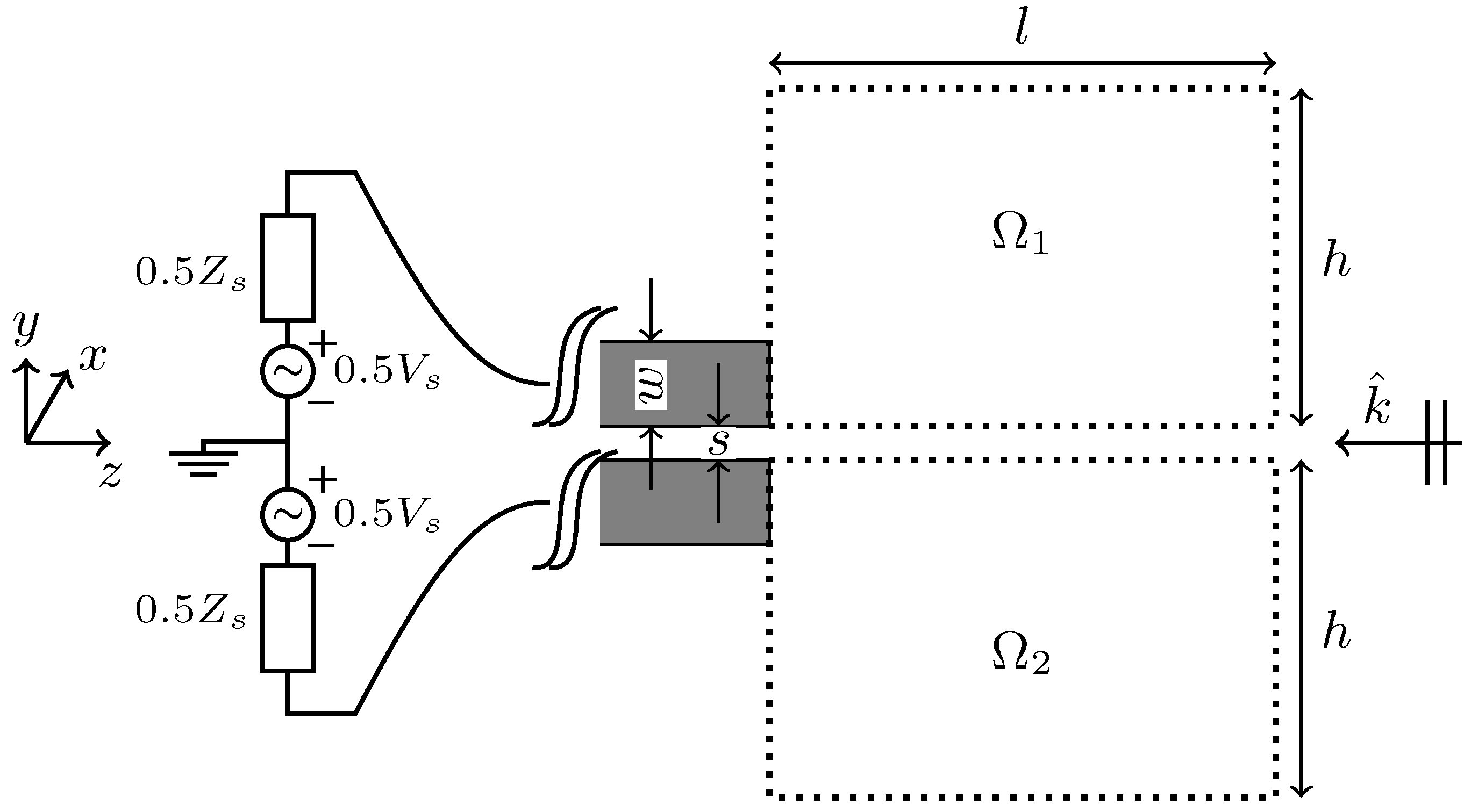
2. Problem Formulation and Numerical Treatment
Figure 1 illustrates the conceptual setup. The design area of the antenna is the domain
, where both
and
have an area
. A differential strip line, printed on a dielectric substrate, feeds the antenna region. The differential line has a line impedance
which can be estimated based on the strip width
w, the strip separation distance
s, and the permittivity of the supporting substrate [
21]. The other side of the differential line is attached to a voltage source with an internal impedance
. Here, we assume that the source and the differential line are matched and both
and
are real. The problem setup entails a mirror symmetry of the model in the
plane. We exploit this symmetry and halve the analysis domain by placing an electric wall at the plane of symmetry. To preserve the matching to the differential line, the source impedance is consequently halved to
[
22]. We remark that
Figure 1 represents a generic differential-feed setup that can be used to model various conventional antenna geometries, such as dipole antennas, travelling wave antennas, and microstrip antennas.
Here, the design objectives are (i) the minimization of the antenna reflection coefficient over the band 6.0–8.5 GHz, (ii) the maximization of the antenna radiation in the positive
z half-space, and (iii) the minimization of the antenna realized gain outside the band of interest. We include the first objective to the optimization problem formulation as the minimization of the energy reflected by the antenna in its transmission mode. The second objective is formulated based on the antenna receiving mode. We include the maximization of the received signals from a set of external plane waves propagating toward the antenna in the
,
, and
directions. This design objective is equivalent to increasing the antenna aperture area over the frequency band of interest and accounting for the specified directivity [
22]. We address the third design objective by maximizing the reflection coefficient of the antenna over neighboring frequencies. For this purpose, we include two additional terms to the objective function to maximize the reflection coefficient at the lower and upper frequencies. We remark that the latter objective results in the minimization of the realized (absolute) gain of the antenna outside the frequency band of interest.
In the transmitting mode, we use the source to excite the antenna with three different signals that impose the energy
,
, and
. The last index refers to the frequency contents of the excitation signal. That is, i, l, and u refer, respectively, to the in-band frequencies, the lower-band frequencies, and the upper-band frequencies. For each excitation, we observe the corresponding outgoing energy,
,
, and
, at the differential line end. In the receiving mode, we excite the model problem by three plane waves propagating in the
,
, and
-directions with the electric field linearly polarized in the
y-direction [
14,
23], and we observe the outgoing energy
at the differential line end. Based on the aforementioned discussion, we formulate the optimization problem
Note that problem (
1) implies the maximization of the factors in the denominator. Problem (
1) reads: seek the distribution of the conductivity values
in the design domain
, enclosed by the dotted lines in
Figure 1, to satisfy the multi-objective function and the constraints.
To compute the factors in problem (
1), we use numerical solutions to Maxwell’s equations by the finite-difference time-domain (FDTD) method [
24]. A coaxial waveguide port, with line impedance
and attached to the differential line end, models the source. We extend the one cell model, previously published by Hassan et al. [
14], to include a square inner probe with size
w (as the strip line width). The reflection coefficient between the coaxial waveguide port and the strip line is below −25 dB over the frequency band of interest. The plane waves excitations are imposed by using the total-field scattered-field formulation [
24].
To solve optimization problem (
1), we rely on the so-called density-based topology optimization approach. The values of the conductivities at each Yee edge (pixel) in the design domain
are subject to design. We allow the design variables to vary continuously between two extreme values that indicate presence or absence of material. Here, these extreme values are the conductivities of a good conductor and a good dielectric. Based on numerical investigations, we consider materials with conductivity
S/m and
S/m as a good conductor and a good dielectric, respectively [
18,
25]. The vector of pixelated conductivities is mapped to a design vector
with entries varying between 0 and 1. Here, the values 0 and 1 represent a good dielectric and a good conductor, respectively. Although the entries of vector
may hold any value between 0 and 1 during the optimization, the final entries must hold either 0 or 1 to allow the fabrication of the design. Allowing the design variables to vary continuously makes it possible to devise adjoint field systems and compute the gradient information of the factors in problem (
1) in an efficient way [
14,
26]. After computing the factors in problem (
1) and their gradient information, we employ Svanberg’s GCMMA algorithm [
27] to iteratively solve problem (
1). Detailed description of the discretization and the numerical treatment can be found in previous work [
14,
18,
28].
3. Results
In the FDTD method, we use a spatial discretization step
of 0.0625 mm, a temporal discretization step
that equals 0.95 of the Courant limit, and 15 cells of a uniaxial perfectly matched layer to simulate the radiation boundary condition. As mentioned in
Section 2, we exploit the problem symmetry to halve the analysis domain. We use a design domain
of area
mm
2, discretized into
Yee faces, which yields
unknown edge conductivities that correspond to the entries of design vector
. To hold the copper distribution, the design domain is backed by a Rogers RO3003 substrate that has a thickness of 0.127 mm, a relative permittivity of 3, and a loss tangent of 0.001 at 10 GHz. The employed differential line has
mm. The frequency bands of interest are the in-band frequencies 6.0–8.5 GHz, the lower-band frequencies 3.5–6.0 GHz, and the upper-band frequencies 8.5–11.0 GHz. To cover these frequency bands, we use time-domain
signals that are truncated after 6 lobes. Each
signal is used to modulate a frequency carrier at the mid of the corresponding frequency interval. We implement the FDTD method to run on graphics processing units (GPUs), and we use uniform FDTD cubical grids in all simulations. We run the numerical experiments on compute nodes equipped with Nvidia V100 GPU cards and with 128 GB internal memory. Based on the current problem discretization, one call to the FDTD solver takes 150 s. We remark that the evaluation of each factor in problem (
1) requires one FDTD simulation, and the evaluation of the corresponding gradient requires one additional FDTD simulation.
First, we solve problem (
1) without including the two filtering factors
and
. That is, the antenna is optimized only for the minimization of the reflected energy
and the maximization of the received energy
from the specified directions.
Figure 2 shows some snapshots illustrating the development of the design during the optimization. We use a uniform initial distribution of the design variables that corresponds to a conductivity of 140 S/m at each Yee edge in the design domain. To secure a connection path between the design domain and the strip line, a square region of area
mm
2 is fixed to be copper at the lower left corner of the design domain. The antenna layout evolves in 136 iterations from a design with large amount of grayness and fuzzy boundaries to a final design with black and white materials as well as crisp boundaries. We stress that each pixel in this design (image) is a design variable, and that such large-scale optimization problem is computationally prohibitive to solve by stochastic optimization techniques, such as genetic algorithms [
29,
30].
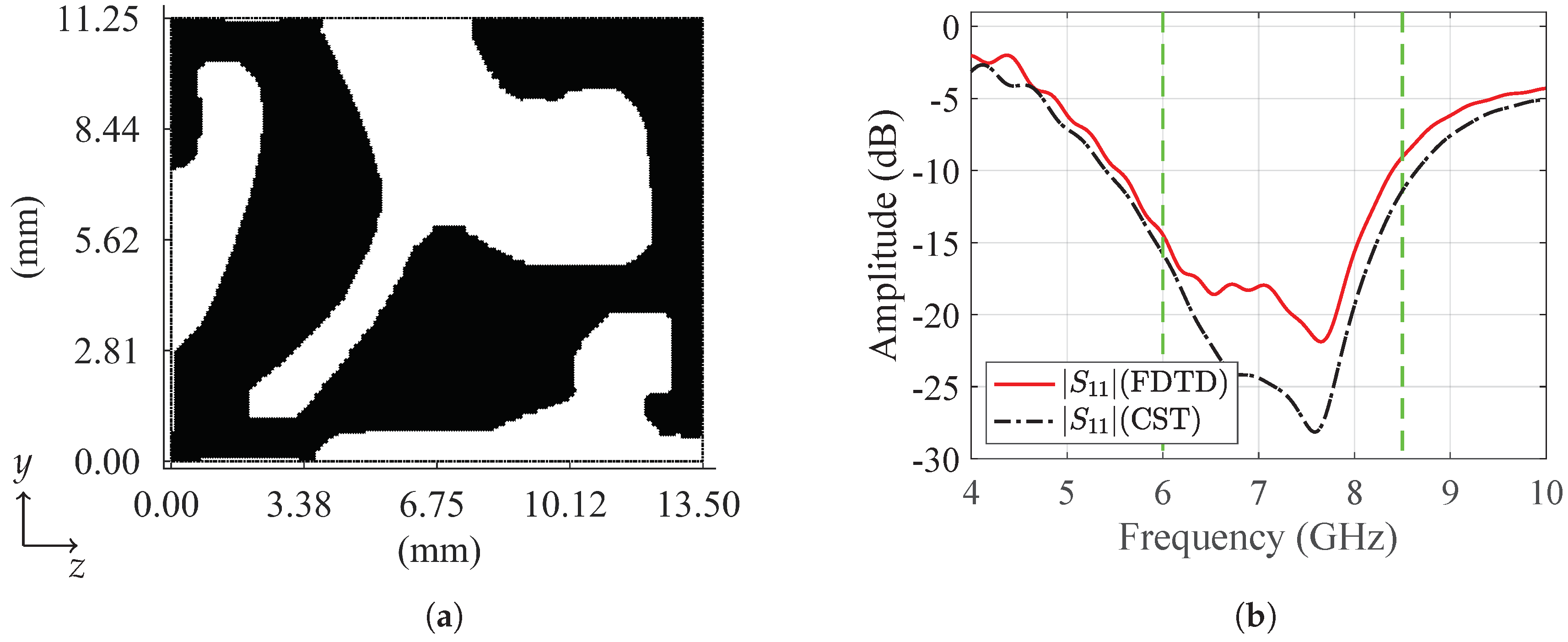
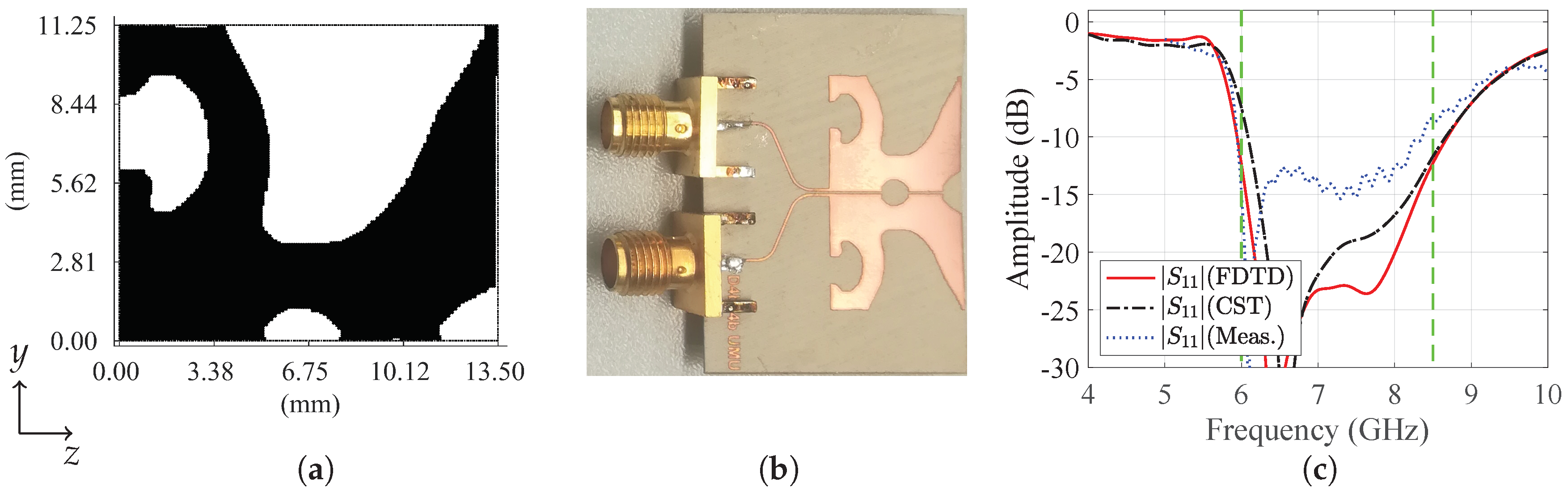
Figure 3a shows the structure of the optimized antenna. The antenna consists of two vertical branches with small cap extensions and a horizontally tapered section inbetween.
Figure 3b shows that the antenna has a reflection coefficient
below −10 dB over the frequency band of interest, marked by the vertical dashed lines. The cross-verification of
shows a good agreement between our FDTD simulation results and the results obtained by the CST commercial package. The antenna has a small reflection coefficient also at frequencies outside the band of interest. More precisely, the antenna reflection coefficient is −13.6 dB and −5 dB at the WiFi frequency 5.8 GHz and at 10 GHz, respectively. We emphasize that the use of a
signal in the excitation of the problem allows targeting the frequency band of interest. However, this choice of excitation does not imply any requirements on the out-of-band frequencies. We use this antenna as a reference to compare with the results presented below.
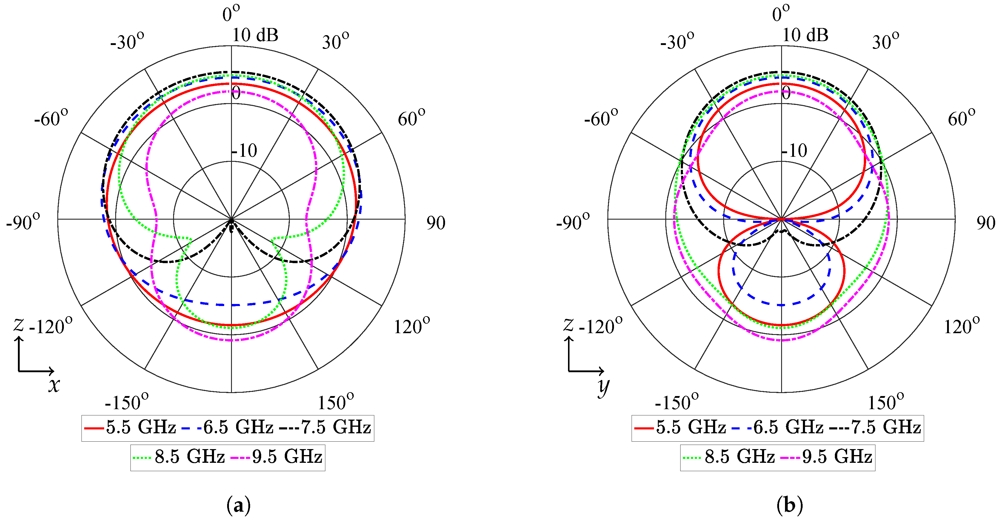
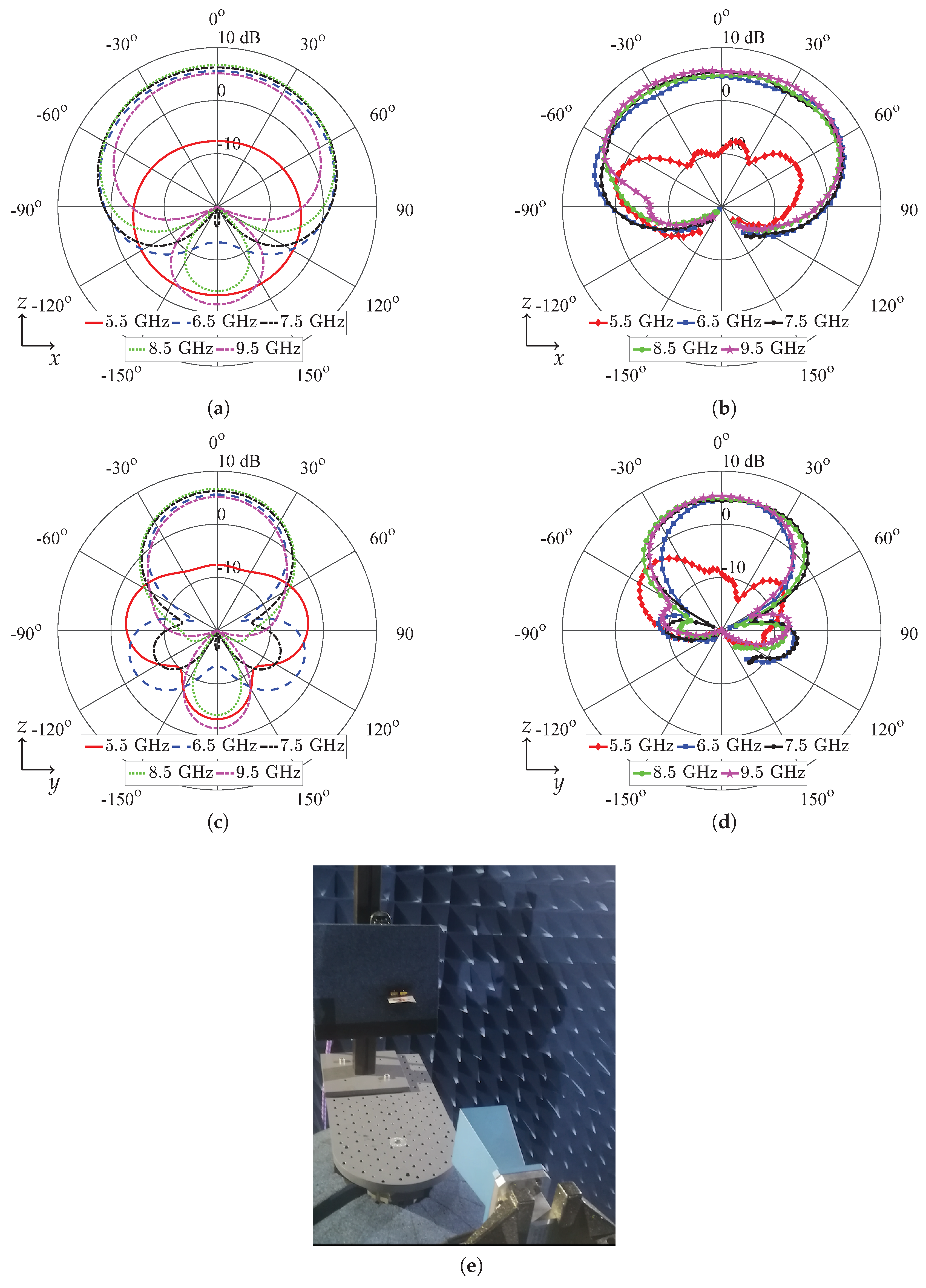
Figure 4a,b show polar plots of the antenna realized gains in the
plane and
plane, respectively. The antenna radiation pattern is slightly narrower in the
plane compared to the
plane. In the two main planes, the cross-polarization level is less than 45 dB, which is a typical feature of differential-fed antennas [
5,
20].
Table 1 summarizes the spatial radiation characteristics of the optimized antenna. The antenna has a maximum gain of
dB within the frequency band of interest, and the gain decreases to 3.4 dB and 2.1 ḋB at 5.5 GHz and 9.5 GHz, respectively. In the
plane, the 3 dB beamwidth decreases as the frequency increases with a smallest value of 124° in the frequency band of interest. In the
plane, the 3 dB beamwidth is essentially stable around 88° ± 2° over the frequency band 6.5–8.5 GHz. Note that in the
plane, as the frequency increases, the antenna pattern forms a radiation dip, which can be clearly seen in the
direction at 7.5 GHz. The angle of this dip moves towards the
x direction (
90°) as the frequency increases. Note that the pattern is more directive towards the
half-space, the direction from which the plane wave excitation impinges.
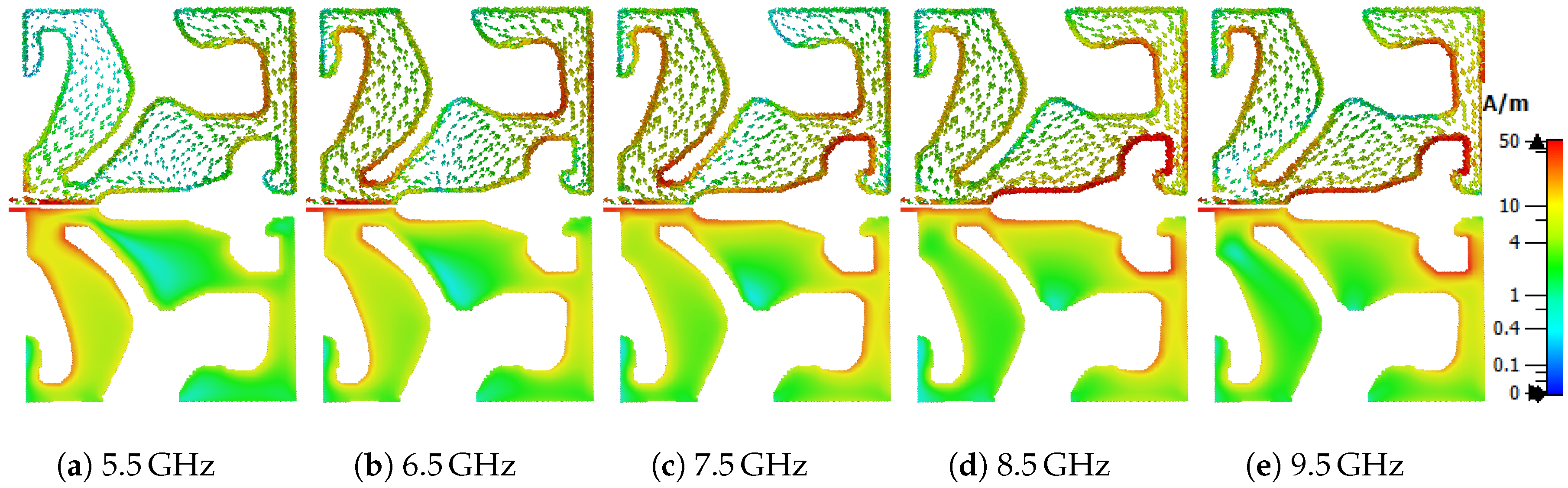
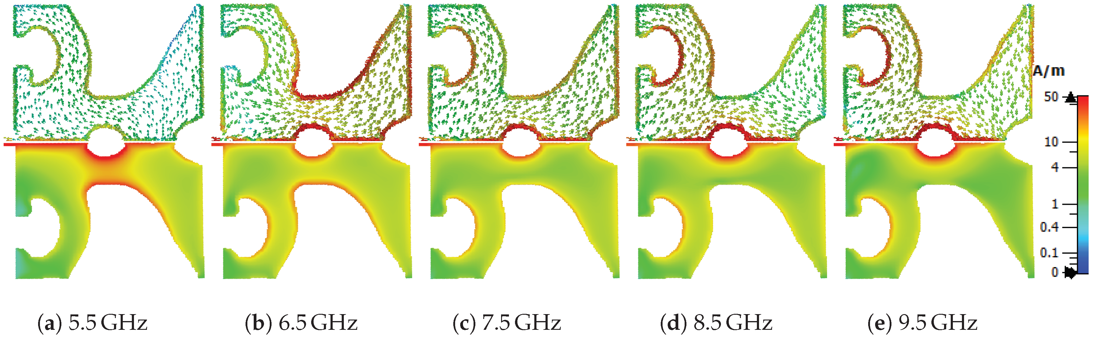
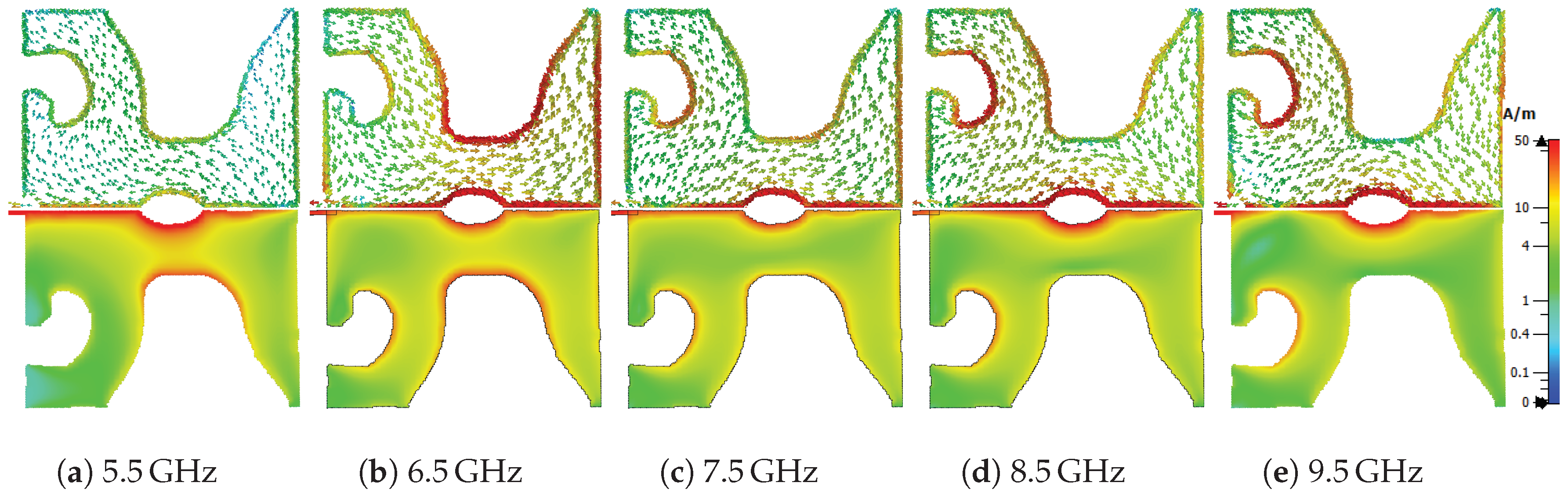
The amplitude of the surface current and its direction determine the overall antenna gain [
22]. To understand the working principle of the optimized antenna, we plot the surface current on the antenna at five frequencies, as shown in
Figure 5.
Figure 5a,e show that the current has different directions on the two vertical branches at 5.5 GHz and 9.5 GHz. In
Figure 5b,c, the surface currents on the two vertical branches have essentially similar amplitudes and directions, which could explain the high gain at 6.5 GHz and 7.5 GHz.
Figure 5d shows that the current has opposite directions on the two branches; however, the peak of the surface current is slightly drifted out towards the external branch. The change of the current directions results in the unexpected decrease of the antenna gain at 8.5 GHz.
Now we solve problem (
1) with all factors of the design objectives included. The snapshots in
Figure 6 show the development of the design during the optimization. Similar to
Figure 2, we start the optimization with a uniform initial distribution. By comparing the two figures, one can see similar trend on the amount of grayness and development of the crisp boundaries. In addition, in both cases, the main layout of the design evolves in the early iterations, and more than 75% of the iterations are used to smoothly remove the grayness in the design and to shape the antenna’s boundaries.
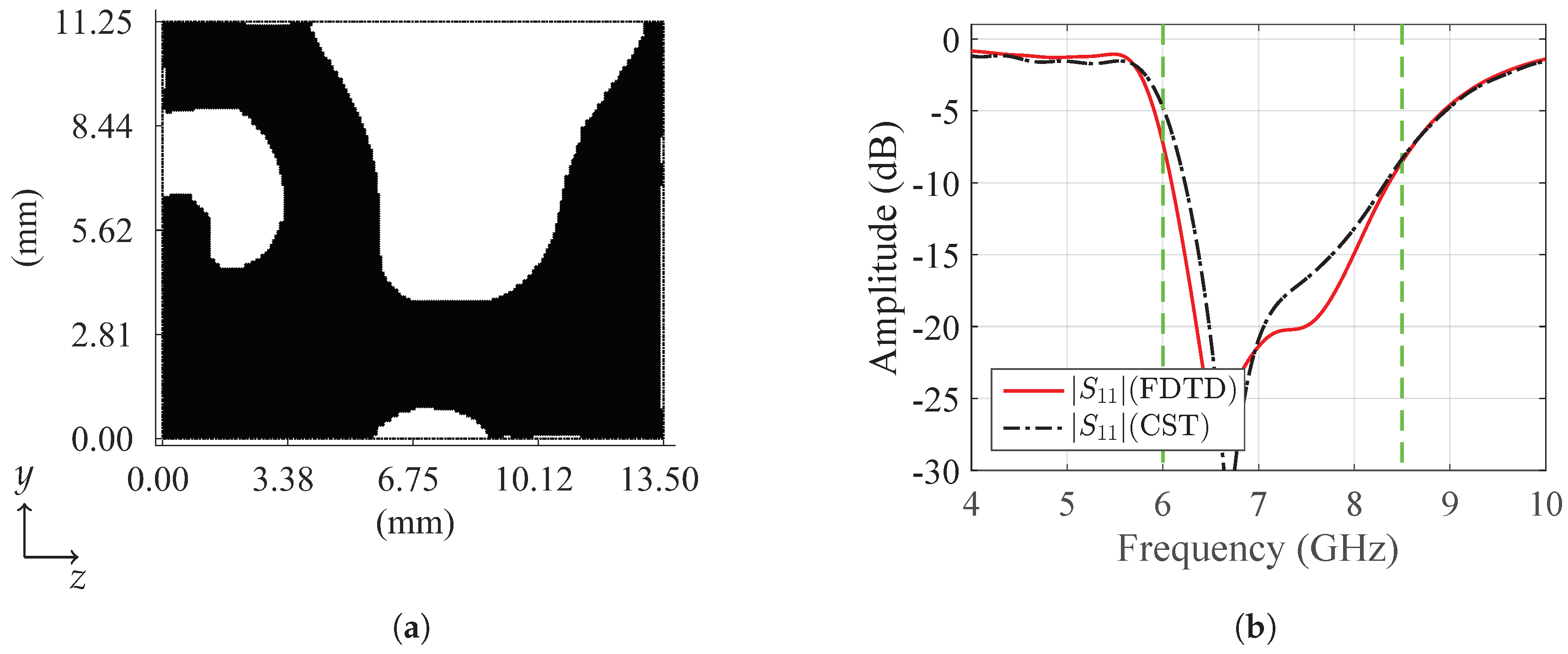
Figure 7a depicts the optimized antenna, denoted Antenna II. The structure consists of two vertical branches with partially tapered boundaries. The two branches are connected by a horizontal strip. The branch near the feeding line has a mushroom-like hollow area. Moreover, a hollow elliptical area is formed beneath the horizontal strip.
Figure 7b shows a manufactured prototype. For measurement purposes, the antenna is connected to a micrsotrip-to-differential line adapter and two SMA connectors, as shown in the figure. We use a ZVA24 Rohde&Schwarz vector network analyzer to measure the antenna reflection coefficient.
Figure 7c shows the antenna reflection coefficient. There is a reasonable match between the measured and simulated results. The antenna has a reflection coefficient around −15 dB over the frequency band 6.2–8.2 GHz. Moreover, the antenna shows a sharp roll-off around 6 GHz. In particular, the antenna has a reflection coefficient of −3.5 dB at the WiFi frequency 5.8 GHz and −2.5 dB at the X-band frequency 10 GHz. Compared to the reference design, this antenna has sharper roll-off at the lower and upper-band edges. However, the band edge at the higher frequencies has a relatively moderate roll-off compared to the lower-band edge. We investigate this issue further below.
Figure 8 shows the realized gain of the optimized antenna at five frequencies.
Figure 8a,b show the simulated and measured gain in the
plane, respectively. Similarly,
Figure 8c,d, respectively, show the simulated and measured gain in the
plane. A photo of the setup for the antenna gain measurement is shown in
Figure 8e. There is a good correlation between the simulated,
Figure 8a,c, and the measured,
Figure 8b,d, gain results. The small angular mismatch between the measured and simulated gain can be attributed to the adapter attached to the antenna during the measurements, which could also explain the slight difference, approximately 1 dB, between the maximum amplitudes of the simulated and measured gain. Note the high suppression level of the antenna gain in the
direction to −7.6 dB at 5.5 GHz. In the
and
planes and over the frequency band 6.5–8.5 GHz, the antenna has essentially a uniform angular gain distribution in the
half-space. The antenna has a maximum simulated gain of
dB in its operational band. The realized gain in the
direction still, however, has a high value of 5.1 dB at 9.5 GHz. The antenna has a 3 dB gain beamwidth above 136° in the
plane, and a stable one, around 64°, in the
plane. The antenna gain characteristics are summarized in
Table 2.
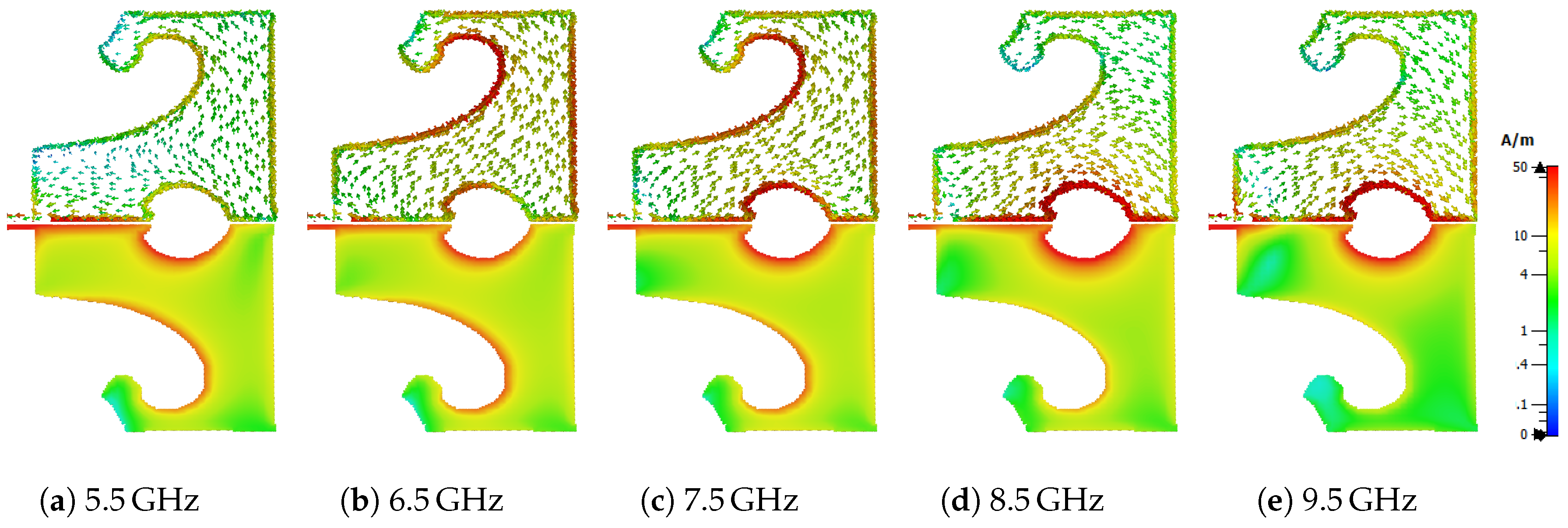
Figure 9 shows the surface current on Antenna II at five frequencies. At 5.5 GHz, the current has its peak at the horizontal strip, around the elliptical hollow slot between the antenna arms, as shown in
Figure 9a. The current amplitude on the vertical branches is relatively small at this frequency, which is why the antenna absolute gain is small. At 7.5 GHz, the current has similar amplitudes and directions on the two branches, as shown in
Figure 9c. At 6.5 GHz and 8.5 GHz, the currents on the vertical branches have opposite directions; however, the current amplitude is higher on the right and the left branches, as shown in
Figure 9b,d, respectively. The net radiation from the antenna is dominated by the branch with the higher current amplitude. Similar to the 6.5 GHz and 8.5 GHz frequencies, the current at 9.5 GHz has different directions on the vertical branches and its peak appears on the left vertical branch, as shown in
Figure 9e.
We attempt to further improve the antenna suppression level at the higher frequencies. To do so, we assign a weighting coefficient to prioritize the factor
over the other factors in problem (
1).
Figure 10 shows one additional design, Antenna III, and its reflection coefficient. In this design, we doubled the weighting of
compared to the previous case. The shape and the performance of the new antenna share many similarities with the previous design. One can see the two vertical branches, the horizontal strip, as well as the slot between the two arms of the antenna. The antenna reflection coefficient has increased to
dB and
dB at 5.8 GHz and 10 GHz, respectively. That is, around a 1 dB improvement compared to the previous design. In the meantime, the antenna still possesses a reflection coefficient below
dB over the frequency interval 6.0–8.5 GHz. The antenna absolute gain, plotted in
Figure 11 and summarized in
Table 3, is
dB over the frequency band 6.5–8.5 GHz. The gain decreases to
dB and 4.0 dB at 5.5 GHz and 9.5 GHz, respectively.
Figure 12 shows the current distribution on Antenna III, which has essentially the same characteristics as Antenna II. We remark that by increasing the weighting coefficient of the upper-band frequencies further, the optimization algorithm might down prioritize the other factors in problem (
1).
Finally, we pursue a numerical experiment to investigate the impact of the design domain area on the solution of problem (
1). We reduce the design domain area from
mm
2 to
mm
2 (34% reduction in area) and solve problem (
1) with the same settings as the previous case. In this case, the discretization of the design domain results in
design variables.
Figure 13 shows the structure of the optimized antenna, Antenna IV, and its reflection coefficient. The antenna structure has one vertical metallic branch, with a tapered outer boundary and a small cap, and the unfilled slot between the two arms still appears. The antenna reflection coefficient is below
dB over the frequency interval 6.0–8.3 GHz,
at 5.8 GHz, and
at 10.0 GHz. Compared to the previous designs, this antenna shows a sharper roll-off at the high band edge. The reduction in the available design space, however, makes it difficult to achieve sharp roll-off at the lower frequencies.
Figure 14 shows that at lower frequencies, Antenna IV has a directional pattern similar to a dipole antenna [
22]. That is, the pattern is approximately omnidirectional in the
plane and a figure-of-eight in the
plane. As the frequency increases, the design area becomes electrically larger, and the antenna shows a more directive pattern in the
direction.
Table 4 summarizes the gain characteristics of Antenna IV.
Figure 15 shows the current distribution on the antenna. At lower frequencies, the current is confined to the vertical branch. At the higher frequencies, the current is confined around the slot between the two arms. This observation illustrates that the vertical branch is responsible for the antenna radiation, and the slot region contributes to the radiation suppression.

 ,
, 


