Article

An Ultra-Wideband Sensing Board for Radio Frequency Front-End in IoT Transmitters

1
Department of Electrical Engineering (ESAT), KU Leuven, 3001 Leuven, Belgium
2
Department of Engineering, University of Ferrara, 44122 Ferrara, Italy
3
Anteverta-mw B.V., 5656AE Eindhoven, The Netherlands
4
Microwave Electronics for Communications, MEC S.r.l, 40127 Bologna, Italy
*
Author to whom correspondence should be addressed.
Electronics 2019, 8(10), 1191; https://doi.org/10.3390/electronics8101191
Submission received: 9 September 2019 / Revised: 9 October 2019 / Accepted: 15 October 2019 / Published: 19 October 2019
(This article belongs to the Special Issue 5G Front-End Transceivers)

Abstract

:
The upcoming technologies related to Internet of Things will be characterized by challenging requirements oriented toward the most efficient exploitation of the energy in electronic systems. The use of wireless communications in these devices makes this aspect particularly important, since the performance of radio transceivers is strongly dependent on the environmental conditions affecting the antenna electrical characteristics. The use of circuits capable of adapting themselves to the actual state of the environment can be a valuable solution, provided that the implemented sensing features have negligible impact on the overall performance and cost of the system. In this work, we present the design and verification of an innovative ultra-wideband sensing board to detect real-time variations of the antenna impedance in transmitters oriented to Internet of Things applications. The proposed sensing board was widely validated by means of small- and large-signal measurements carried out at microwave frequencies.

Graphical Abstract

1. Introduction

Internet of Things (IoT) has become more and more common nowadays in the research community. Starting from [1,2], where the main concepts of IoT were addressed, the research around this topic has grown and, consequently, additional details have been defined about the requirements (e.g., low cost, energy efficiency, broad bandwidth).
The basic idea about IoT is that things or objects become smart, which means that they obtain the ability to interact with each other and work together, even exploiting the capabilities of the internet network. The innovation regarding IoT is not necessarily related to the development of new electronic systems but also to the need to adapt existing systems by adding these smart functionalities.
IoT devices will be used in applications for our daily life at home or in the industry. For instance, home devices include smart TVs, speakers, wearables, and smart appliances, whereas technologies dedicated to security systems and to sensor and monitor traffic or weather are dedicated to the industry [3]. The communication between devices can be delegated to common standards, such as multiband WLAN [4,5], although ultra-wideband (UWB) transmissions are nowadays spreading out as an effective solution, especially for short-range communications [6,7,8,9]. Their use is defined by strict regulations, since they exploit bandwidths already used by other services and applications and, therefore, the transmitted power must be limited to avoid any interference. For example, the US and European regulations allow UWB transmissions from 3.1 to 10.6 GHz with a maximum power of −41 dBm/Hz over a bandwidth of at least 500 MHz or 20% of the center frequency [9,10].
Due to the vastness of possible applications, IoT capabilities should be integrated in low-cost objects and deployed under a huge variety of conditions. An important goal will be to equip these devices with the capability to adapt themselves according to the actual operating condition, in order to provide stable performance regardless of any environmental variation.
Considering the radio communication environment for the aforementioned applications, the antenna near-field may change drastically in real operating conditions, and this will affect the antenna input impedance. This variation has the strongest impact at the transmitter side (composed of an antenna, a radio frequency (RF) front-end, and digital signal processing), especially on the RF front-end (e.g., power amplifier (PA)). Indeed, the antenna load variation jeopardizes the PA performance, for example, through reducing efficiency, gain, and linearity. In addition, a strong mismatch condition may have a considerable and detrimental impact on the system reliability, since it could lead to the active devices in the PA being close to their maximum rating specifications [11,12].
This is not the first time that this problem has been faced. Indeed, several approaches have been proposed in the literature to solve the mismatch problem between the PA and the antenna, including enhancement of the circuit architecture [13], reconfigurable matching networks [14], and signal adaptation. These approaches are not all compatible with IoT requirements: for example, making the circuit design more robust by means of an isolator would create additional losses which are not in line with the energy-efficiency goal of IoT.
In this work, we will assume the PA is an off-the-shelf component, having no tight specifications in terms of robustness to load variations. We also assume that the load presented to the PA can be adjusted in real time by means of a reconfigurable matching network (RMN) (Figure 1). In this scenario, the possibility of monitoring the RF front-end load condition to possibly compensate for load variations by means of the RMN is a crucial aspect for maximizing the overall performance of the system.
RMNs can be implemented by using different technologies, such as switches, to select between stubs [15] or capacitors [16], microelectromechanical systems (MEMS) [17], and semiconductor varactors [18,19]. Whatever the choice, sensing of the antenna impedance is required in order to properly tune the RMN. To achieve this, multiple techniques have been proposed in the literature. The most common solutions can be divided into two main groups: those focusing on monitoring the amplitude only and with narrowband specification, and those with phase information and broadband implementation [20,21]. However, both approaches are not compatible with IoT devices. The first is not suitable because of the need for vectorial information over a large bandwidth. The second, despite being broadband, adopts a quadrature down converter which creates additional losses and power consumption. Another example is a commercial gain/phase detector [18,22] to acquire the reflection coefficient of the antenna. Being an active device, it requires a DC supply, which is clearly not suitable for low-cost high-efficiency applications.
In this paper, the proposed approach consists of an ultra-wideband passive network able to detect the load variations in terms of both amplitude and phase. It is based on a six-port junction [23,24], which is a passive structure. It has been designed to achieve a bandwidth of 1 GHz, i.e., from 5 to 6 GHz, covering the unlicensed national infrastructure (U-NII) radio bands, the 5 GHz Wi-Fi band, and to be suitable for 802.11ac Wi-Fi access points (ACs). The availability of such a large bandwidth is a great advantage in terms of the possible applications, since it can be used to accommodate different services using the same RF front-end and antenna system, e.g., UWB localization [25] with 5-GHz WLAN capabilities for data transmission. To our best knowledge, this is the first time that such a kind of device is presented for an IoT wideband RF transmitter application.
This paper is organized as follows. In Section 2, the six-port junction and the detector topology and design are explained as well as the fabrication procedure. In Section 3, the sensing board performance is validated by means of measurements. The fabricated device will be tested not only to verify its capability to achieve the correct impedance information but also in terms of nonlinearity and bandwidth. Finally, in Section 4, some conclusions will be drawn.

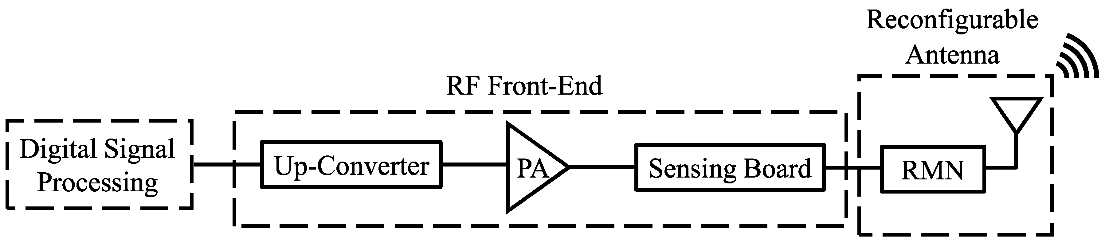
2. Sensing Board Design

The block scheme of the proposed sensing technique for the detection of the front-end load impedance variations is shown in Figure 2. The six-port junction [23,24] solution has been chosen because it is simple to construct, low-cost, meets broadband requirements, and does not require any power supply. All of these aspects are compatible with IoT devices. The concept behind this passive structure is well-known in the literature [23,24], and it has already been used in various microwave and wireless applications, including reflectometers and direct conversion receivers for communication.
The power detectors associated with the six-port junction are designed to get the baseband voltages which are used to calculate the reflection coefficient of the antenna. They also respect the IoT requirements, i.e., wideband operation related to the adopted bandwidth and no need for a power supply.
This design covers a bandwidth of 1 GHz, from 5 to 6 GHz. In the following subsections, we will describe the design of these elements in detail.

2.1. Six-Port Junction Design

The six-port junction can be seen as a black box with one input and five outputs (see Figure 3). Four output ports will be connected to four power detectors providing four voltages from which the antenna reflection coefficient can be retrieved in terms of amplitude and phase through an appropriate calibration algorithm. We will describe this aspect in Section 2.3.
In the literature, it is possible to find several solutions for the design of a six-port junction. In our case, considering the demand of a simple structure, we adopted the one described in [26]. As shown in Figure 3, it has one input port, which is connected to the power amplifier (P1), whilst the five output ports are connected respectively to the reconfigurable antenna (P2) and to the power detectors (P3, P4, P5, P6).
In Figure 3, the six-port junction is composed of several passive elements: a 12 dB directional coupler, a Wilkinson power divider, three 90° hybrid couplers, and a 3 dB attenuator. The choice of the 12 dB coupling factor (CF) for the directional coupler was made as a tradeoff between cost and accuracy of the power detectable at the four output ports. Indeed, by increasing the CF, the calibration algorithm of the six-port junction is more sensitive to errors, and this will impact the reading of the unknown load [23,24].
The design was considered over a wideband frequency range starting from 5 to 6 GHz [27] and carried out using a commercial CAD environment (i.e., Keysight ADS [28]); electromagnetic simulations (i.e., Keysight Momentum, embedded in Keysight ADS) were extensively adopted to increase the accuracy of the design.
The board was manufactured on a Rogers R04350B low-cost PCB substrate with a dielectric constant of 3.48 and a thickness of 0.508 mm. The fabricated board is shown in Figure 4.

2.2. Detector Design

The aim of the power detector is to convert RF power into DC power [29]. A power detector is needed at the six-port junction output ports dedicated to sense the antenna reflection coefficient (i.e., ports P3, P4, P5, and P6 in Figure 4). The classical RF power detector is composed of a diode, a low-pass filter (LPF) formed by a load resistor ( R L o a d ) and a capacitor ( C L o a d ), and an input matching network (IMN), as shown in Figure 5.
In this work, we used a Skyworks SMS7630-079 LF zero-bias Schottky diode from (emission coefficient n = 1, reverse saturation current Is = 5 μA at 25°).
The choice of R L o a d was carried out by means of harmonic balance simulations performed with Keysight ADS over the entire bandwidth (from 5 to 6 GHz). Since no IMN was designed, the input power has been swept over a wide range, i.e., from −20 to +20 dBm, in order to compensate for the input mismatch.
The resistance R L o a d has been selected to maximize the output voltage by sweeping its value from 36 Ω to 36 kΩ. The upper value was chosen considering the quality of available off-the-shelf resistors in terms of parasitic contributions in the entire frequency band of interest.
As shown in Figure 6, the output voltage is directly proportional to the R L o a d value. From this plot, we chose as best value R L o a d = 36 kΩ since it gives a higher value of the output-detected voltage. This choice will increase the accuracy of the power detection. Using the results from Figure 6, we can also estimate the saturation region of the detector, which happens approximately at 9 dBm of input power for the selected impedance. This point, which will be affected by the input matching network, is expected to be beyond the actual power level that will reach the detector. However, the validation of the final design will include an analysis of the behavior of the complete sensing board for realistic power levels, to verify if saturation effects arise from the detector nonlinearity.
After determining R L o a d , the other parameter to be addressed is C L o a d . Its value can be determined by looking at the desired bandwidth of the LPF. It is defined by the first-order LPF formed by R L o a d in parallel (considering the low-frequency operation of the LPF) to the differential diode resistance R d and the capacitor C [30,31].
For this purpose, by looking at Equation (1),
f 3 d B = 1 2 π R t o t C L o a d , R t o t = R d R L o a d ,
it is possible to determine C L o a d . Since the proposed reflectometer is designed to be cheap and accurate, the idea is to guarantee the possibility of analyzing the antenna impedance variation in 1 GHz bandwidth using narrowband test signals. For example, the entire bandwidth can be swept by using a single-tone signal over the grid of frequencies for which the calibration has been performed. This quickly provides the impedance of the antenna, which can be directly used to control the RMN to optimize the matching condition. As a matter of fact, the principle is the same of a spectrum analyzer that can explore very large bandwidths, preserving high accuracy levels and dynamic range, by exploiting narrowband IF filters. To achieve this, we design the LPF to obtain a bandwidth that is small enough to preserve the accuracy of the power detection, although not too narrow to avoid excessive inertia of the filter, which would slow the frequency sweep. We chose f 3 d B = 15 kHz as a good tradeoff, for which R L o a d = 36 kΩ and C L o a d = 2.7 nF are required.
The last step in the detector design is related to the IMN, whose goal is to ensure the maximum power transfer to the diode. It has to cover the entire frequency range (from 5 to 6 GHz) and all the expected power values (from −20 to 0 dBm). The power range is now reduced because of the actual power level we expect at the output port of the six-port junction under actual operating conditions (i.e., input power of 10 dBm).
To our best knowledge, it is the first time that the IMN of the detector is designed for 1 GHz of bandwidth since, in typical applications [30,31], a narrowband design is adopted. The IMN used for this detector design is shown in Figure 7 and makes use of a bridged tee [32], an RLC matching network, commonly used for broadband cascadable gain stage design. This kind of network transforms the input impedance of the loaded detector diode to the required 50 Ω system impedance by absorbing its reactive part into an all-pass filter over a very broad frequency band [32]. The inductors (L1 and L2), the capacitor (C) and the resistance (R) values of the bridged tee are easily calculated from the design equations reported in [32] and their values are: L1 = 0.36 nH, L2 = 0.44 nH, C = 0.080 pF, and R = 50 Ω.
Due to the high-frequency application, the lumped components have been replaced with distributed ones designed in microstrip technology, avoiding the unwanted parasitic effects of lumped SMD components. In particular, inductors are realized with short transmission line length, and the series capacitor is implemented with an interdigitated structure due to its small capacitance value. The 50 Ω resistor, instead, is a high frequency SMD flip-chip thin-film component.
A broadband RF short circuit has been realized at the diode output by means of a radial stub to filter out the residual fundamental frequency and the harmonic components.
Each detector was designed considering the same Rogers substrate already used for the six-port junction (see Figure 8). The detector boards have been fabricated separately from the six-port junction for testing purposes. Nevertheless, the use of the same substrate allows for easy integration of all the elements of the sensing board over the same PCB.

2.3. Calibration Algorithm

The most important issue in the design of the proposed sensing board is the calibration algorithm [26] whose main aim is to derive the reflection coefficient of the load cascaded to the sensing board (i.e., the antenna) from the voltages provided by the detectors.
In the literature, it is possible to find plenty of algorithms dedicated to the six-port calibration [26]. In this work, we adopted the five-standard calibration method, based on a linear approach [33]. It can be easily implemented in a common programming language (e.g., C++, MATLAB), and since it is not computationally expensive, it is suitable for a simple IoT device.
The algorithm consists of a set of mathematical matrix calculations. The main step is the calculation of the matrix C , which characterizes the six-port junction. It is a 4 × 4 real matrix that links the vector of the four read powers P   =   [ p 3 , p 4 , p 5 , p 6 ] T to the unknown load vector Γ   =   [ 1 , | Γ | ,   R e ( Γ ) ,   I m ( Γ ) ] T according to the following relationship [26,33]:
P = ρ C Γ ,
where ρ = | b 2 | 2 is the incident wave power at the antenna input port (i.e., antenna in Figure 2).
The calibration of the six-port junction is based on the identification of C by means of the measurement of the vector P for five known loads used as a reference. Then, the generic unknown load can be derived by using the matrix X = C 1 according to the following equations [26]:
R e ( Γ ) = j = 1 4 x 3 j P j + 2 j = 1 4 x 1 j P j + 2     I m ( Γ ) = j = 1 4 x 4 j P j + 2 j = 1 4 x 1 j P j + 2 ,
where P j is the power value at port j when measuring the unknown load, and x i j are the elements of X .
The five calibration loads should be chosen in order to maximize the accuracy and the stability of the algorithm. In our practical case, we chose an experimental approach for the selection of these loads. Taking into account the application for the sensing board, we considered some impedance measurements of a dedicated 5.15–5.85 GHz antenna array for high data rate ultra-short-range 3 × 3 multiple input multiple output (MIMO) wireless communications [34]. The antenna impedance was measured in three different configurations, i.e., as: a standalone antenna, integrated in a worktop, and mounted underneath the worktop. The measurement results are shown in Figure 9.
Starting from these three possible conditions, we chose five loads to optimize the accuracy of the sensing-board algorithm in the area defined by the impedances reported in Figure 9 over the entire bandwidth. In addition, we took into account the condition number of the matrix C [35] to reduce the sensitivity of the calibration algorithm to measurement uncertainty. The selected loads are reported in Table 1, for which the condition number results sufficiently small (~5).
Matrix C (and, therefore, matrix X ) must be calculated for each frequency of interest. This is a time-consuming operation, especially if a small frequency resolution is required over the entire design bandwidth. Moreover, it requires the availability of the five “standards” designed over a wide frequency range.
We propose a different approach which is sufficiently accurate and less time consuming, since it is implemented via simulation, e.g., by using Keysight ADS. We reproduce the response of the sensing board modeled by the measured S-parameters for the six-port junction and the electromagnetic simulation together with the detector diode nonlinear model. We connect at port 2 (P2, Figure 4) each calibration loads for the all frequencies of interest (e.g., from 5 to 6 GHz with a step of 100 MHz) to obtain the four output voltages. Then, matrix C and the calibration algorithm are implemented via MATLAB starting from the simulation results. Apart from the time reduction compared with the long measurement process, one additional advantage is the possibility to perform this procedure without the need for real dedicated calibration loads or equivalent elements (e.g., a passive tuner) for the synthesis of the required impedances, which reduces the cost of the procedure.
Using such an implementation, the calibration procedure that leads to matrix C should be performed only once, and then the result can be stored as matrix X = C 1 to directly use Equation (3) for the impedance detection. Since this matrix is composed of 16 real floating-point numbers, assuming a 32-bit representation, only 64 bytes of memory are required for each calibrated frequency. From a computational point of view, Equation (3) only requires 16 multiplications, 12 additions, and 2 divisions for each frequency we want to detect the reflection coefficient. Such a limited number of operations and memory requirements are today largely satisfied by common low-cost microcontrollers, which can be suitable for the applications we are addressing.
Considering Equation (3), the power needs to be calculated from the detector output voltages. To this purpose, an analysis was done to evaluate the nonlinearity of the detector (see Section 3.3.1).

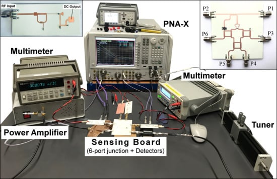
3. Measurement Section

In this section, the measurements for the test and validation of the sensing board are reported.

3.1. Validation of the Fabricated Boards

S-parameter measurements have been carried out to validate the accuracy of the six-port junction [27]. We performed them with a Keysight PNA-X in the bandwidth from 4 to 7 GHz, and reported the results in Figure 10. From [23,24], the paths between P3–P1 and P6–P1 and between P5–P1 and P4–P1 have to be equal, and these requirements are approximately satisfied over the whole bandwidth, notably in the targeted frequency range (5–6 GHz). In Figure 10, we also report the insertion loss of the six-port junction, which is approximately constant and equal to 1 dB over the band of interest.
The return loss of the fabricated detector prototypes was measured at different power levels to verify the effectiveness of the matching network as a function of power over the entire bandwidth. The results reported in Figure 11 show a return loss of −15 dB or less, close to the central frequency (5.5 GHz). It is noteworthy how the designed matching network strongly reduces the variation of the return loss over a considerable range of input power.

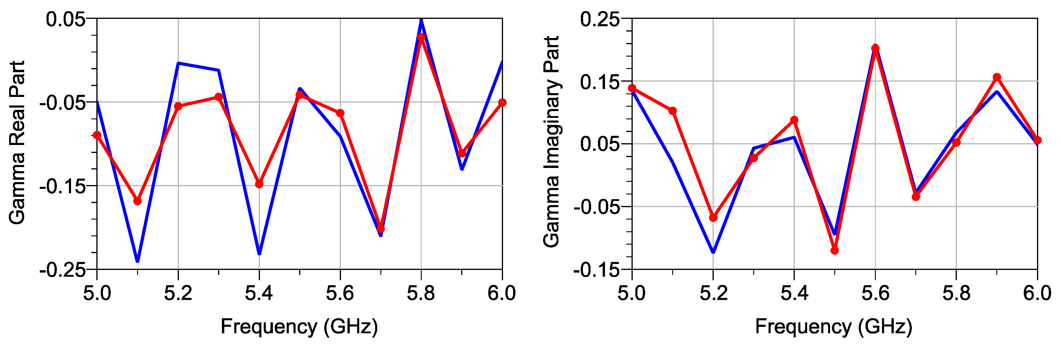
3.2. Validation of the Impedance Detection

In this section, a validation of the designed sensing board as a reflectometer is performed with the setup shown in Figure 12, which includes an RF microwave source (Keysight N5182B), a Maury microwave mechanical tuner, and a digital multimeter (Rigol DM3058). By means of a set of single-tone measurements, from 5 to 6 GHz with 100 MHz steps, we are able to test the sensing board (six-port junction + detector) over the entire bandwidth of interest. These measurements were carried out by applying one tone for each frequency with a constant input power of 10 dBm (8.27 dBm at the sensing board input port) and settling the impedance values by a mechanical tuner in order to avoid any change due to the interactions with the environment that would be produced by an actual antenna. These impedances were measured in advance by means of a vector network analyzer to gather their values with a high level of accuracy, so that they can be considered a good reference for the validation of the sensing board. The read voltages from the multimeter were processed and, through the calibration algorithm explained in Section 2.3, the load reflection coefficients were derived. These results are reported in Table 2 and in Figure 13. We can conclude that the detected impedances are in good agreement with the ones set by the mechanical tuner over the investigated bandwidth.

3.3. Sensing Board Validation with Large-Signal Measurements

In this section, a nonlinearity analysis of the sensing board and a bandwidth estimation of the detectors are carried out. To perform both analyses, two different measurement setups were used.

3.3.1. Nonlinearity of Detectors and Sensing Board

Looking at Equation (2), we need to know the power at the four output ports of the six-port junction in order to retrieve the information about the load reflection coefficient. They can be measured through a power meter as in [27] or with the setup implemented in [36], which basically works as the power detectors.
Considering the designed sensing board, we should retrieve the power values from the output voltages of the detectors. The direct use of the well-known proportionality between power and squared voltage ( P V 2 ) is correct only from a theoretical perspective. In practice, the nonlinearity of the detectors can alter this relationship, causing a poor level of accuracy in the determination of the load impedance. As a consequence, the P i n V o u t characteristic of the detectors has to be properly characterized in order to obtain accurate results over a wide range of power values.
It should be pointed out that a nonlinear verification of the detectors is required even if the RF front-end is intended to operate at constant power. Indeed, the power level reaching the four detectors of the sensing board is not the same for every port of the six-port junction and, in general, depends on the actual front-end load.
By characterizing the detectors P i n V o u t relationship, we can extend the sensing board operation over a considerably wide range of power. To this end, we used the setup in Figure 14. A Keysight PNA-X, in nonlinear vector network analyzer (NVNA) mode, has been used to perform nonlinear measurements on the sensing board with an input power sweep from −10 to 25 dBm. To obtain the highest levels of power, it was necessary to introduce a power amplifier (frequency range 2 to 8 GHz, gain 35 dBm, P 1 d B m = 34 dBm). Through two directional couplers, one at the input and one at the output, it is possible to retrieve the incident and reflected waveforms at the input and the output ports of the sensing board from which the actual input power and the load reflection coefficient can be calculated. The voltages at the four output ports of the sensing board are detected by means of two multimeters (Rigol DM3058 and Hewlett Packard 34401A). As load, we used a mechanical tuner.
The results from these measurements are reported in Figure 15. Here, the frequency is constant at 5.5 GHz, the input power sweeps from −10 to 25 dBm and the impedance set by the tuner is Z t a r g e t = 63 j   19   Ω . We used the P i n V o u t characteristic of the detectors to estimate the actual power delivered by the four output ports of the six-port junction.
As expected, the detected impedance is approximately constant over the whole range of input power, and data results agree with the value set by the tuner. This confirms the usefulness of the introduction of the detector P i n V o u t actual characteristic in the calibration algorithm of the sensing board to extend its functionality to a wide range of power.

3.3.2. Bandwidth of the Detector

In this section, we verify the bandwidth of the detector. For this purpose, the measurement condition must be properly defined. The low-pass behavior of the detector cannot be investigated by using single-tone measurements. In fact, the 5 to 6 GHz RF IMN prevents low-frequency signals from flowing through the circuit, whereas an RF sinusoid will provide only a constant output voltage. To solve this problem, the idea was to use the detector to reveal the envelope of a 2-tone signal by varying the frequency of the envelope itself to characterize the frequency response of the output LPF.
We used the setup shown in Figure 16, where an RF source (Keysight N5182B) is used to set a two-tone signal at the input of the detector board, and an oscilloscope (Tektronix DPO4104) acquires the output waveform. For the 2-tone signal generation, we consider the central frequency f 0 of 5.5 GHz and we swept the distance Δ f between the two tones from 200 Hz to 40 kHz.
To evaluate the real bandwidth of the detector, the output waveform is processed through a mathematical procedure to calculate the peak-to-peak voltage for each value of Δ f . The results are reported in Figure 17. The cutoff frequency (−3 dB point) is approximately 13.4 kHz, which is in good agreement with our design specification (i.e., 15 kHz).

4. Conclusions

In this work, we have described an ultra-wideband sensing board for IoT applications. We have extensively characterized the sensing board by means of small- and large-signal measurements in the frequency range of interest (i.e., 5 to 6 GHz) to deeply verify the goodness of the proposed design approach. In particular, we have also investigated the sensing board nonlinear behavior and verified the possibility of extending its application to a wide range of power levels.

Author Contributions

Investigation, A.P. and G.B.; Methodology, A.R., G.A. and D.R.; Supervision, A.R., G.V. and D.S.; Writing—original draft, A.P. and G.B.; Writing—review & editing, A.R., D.R., G.A., G.V. and D.S.

Funding

This research was funded in part by the Eurostars project E!10149 MicromodGaN.

Conflicts of Interest

The authors declare no conflict of interest.

References

  1. Bandyopadhyay, D.; Sen, J. Internet of Things: Applications and Challenges in Technology and Standardization. Wirel. Pers. Commun. 2011, 58, 49–69. [Google Scholar] [CrossRef]
  2. Jo, M.; Maksymyuk, T.; Batista, R.L.; Maciel, T.F.; de Almeida, A.L.F.; Klymash, M. A survey of converging solutions for heterogeneous mobile networks. IEEE Wirel. Commun. 2014, 21, 54–62. [Google Scholar]
  3. Minoli, D.; Occhiogrosso, B. Ultrawideband (UWB) Technology for Smart Cities IoT Applications. In Proceedings of the IEEE International Smart Cities Conference, Kansas City, MO, USA, 16–19 September 2018; pp. 1–8. [Google Scholar]
  4. ETSI EN 301 893. 5 GHz RLAN; Harmonised Standard Covering the Essential Requirements of Article 3.2 of Directive 2014/53/EU; ETSI EN: Sophia Antipolis, France, 2014. [Google Scholar]
  5. Huang, C.P.; Christainsen, K.; Nabokin, S.; Mirzayantz, R.; Allum, J.; Chen, A.; Lam, L.; McPartlin, M.; Doherty, M.; Vaillancourt, B. A highly integrated single chip 5–6 GHz front-end IC based on SiGe BiCMOS that enhances 802.11ac WLAN radio front-end designs. In Proceedings of the IEEE Radio Frequency Integrated Circuits Symposium (RFIC), Phoenix, AZ, USA, 17–19 May 2015; pp. 227–230. [Google Scholar]
  6. Salpietro, R.; Bedogni, L.; di Felice, M.; Bononi, L. Park Here! a smart parking system based on smartphones’ embedded sensors and short range Communication Technologies. In Proceedings of the IEEE 2nd World Forum on Internet of Things (WF-IoT), Milan, Italy, 14–16 December 2015; pp. 18–23. [Google Scholar]
  7. Lukić, M.; Mihajlović, Ž.; Mezei, I. Data Flow in Low-Power Wide-Area IoT Applications. In Proceedings of the 26th Telecommunications Forum (TELFOR), Belgrade, Serbia, 21–22 November 2018; pp. 1–4. [Google Scholar]
  8. Pal, A.; Kant, K. NFMI: Connectivity for Short-Range IoT Applications. Computer 2019, 52, 63–67. [Google Scholar] [CrossRef]
  9. ETSI EN 302 065-5. Short Range Devices (SRD) Using Ultra Wide Band Technology (UWB); Harmonised Standard Covering the Essential Requirements of Article 3.2 of Directive 2014/53/EU; Part 5: Devices using UWB technology onboard aircraft; ETSI EN: Sophia Antipolis, France, 2014. [Google Scholar]
  10. Ramos, A.; Lazaro, A.; Girbau, D.; Villarino, R. RFID and Wireless Sensors Using Ultra-Wideband Technology; ISTE Press—Elsevier: London, UK, 2016; pp. 14–16. [Google Scholar]
  11. Raffo, A.; di Falco, S.; Sozzi, G.; Menozzi, R.; Schreurs, D.M.M.-P.; Vannini, G. Analysis of the gate current as a suitable indicator for FET degradation under nonlinear dynamic regime. Microelectron. Reliab. 2011, 51, 235–239. [Google Scholar] [CrossRef]
  12. Vadalà, V.; Bosi, G.; Raffo, A.; Vannini, G.; Avolio, G.; Schreurs, D.M.P. Influence of the gate current dynamic behaviour on GaAs HEMT reliability issues. In Proceedings of the 7th European Microwave Integrated Circuit Conference, Amsterdam, The Netherlands, 29–30 October 2012; pp. 258–261. [Google Scholar]
  13. Pozar, D.M. Microwave Engineering, Reading; Addison-Wesley: Boston, MA, USA, 1990; pp. 529–565. [Google Scholar]
  14. Mohamed, A.M.M.; Boumaiza, S.; Mansour, R.R. Novel Reconfigurable Fundamental/Harmonic Matching Network for Enhancing the Efficiency of Power Amplifier. In Proceedings of the 40th European Microwave Conference, Paris, France, 28–30 September 2010; pp. 1122–1125. [Google Scholar]
  15. Nawaz, A.A.; Albrecht, J.D.; Ulusoy, A.C. A Ka-Band Power Amplifier with Reconfigurable Impedance Matching Network. In Proceedings of the IEEE 19th Topical Meeting on Silicon Monolithic Integrated Circuits in RF Systems (SiRF), Orlando, FL, USA, 20–23 January 2019; pp. 1–3. [Google Scholar]
  16. Chen, H.; Hsieh, Y.; Lu, L. A 5.5-GHz multi-mode power amplifier with reconfigurable output matching network. In Proceedings of the IEEE Radio Frequency Integrated Circuits Symposium (RFIC), Phoenix, AZ, USA, 17–19 May 2015; pp. 203–206. [Google Scholar]
  17. Lu, Y.; Peroulis, D.; Mohammadi, S.; Katehi, L.P.B. A MEMS reconfigurable matching network for a class AB amplifier. IEEE Microw. Wirel. Compon. Lett. 2003, 13, 437–439. [Google Scholar]
  18. Baroni, A.; Nepa, P.; Rogier, H. Wearable self-tuning antenna for emergency rescue operations. IET Microw. Antennas Propag. 2016, 10, 173–183. [Google Scholar] [CrossRef]
  19. Hur, B.; Eisenstadt, W.R.; Melde, K.L. Testing and Validation of Adaptive Impedance Matching System for Broadband Antenna. Electronics 2019, 8, 1055. [Google Scholar] [CrossRef]
  20. Ji, D.; Jeon, J.; Kim, J. A Novel Load Insensitive RF Power Amplifier Using a Load Mismatch Detection and Curing Technique. In Proceedings of the 2013 IEEE Radio Frequency Integrated Circuits Symposium (RFIC), Seattle, WA, USA, 2–4 June 2013; pp. 341–344. [Google Scholar]
  21. Curticipean, F.; Niittylahti, J. An Improved Digital Quadrature Frequency Down-Converter Architecture. In Proceedings of the 1977 11th Asilomar Conference on Circuits, Systems and Computers, Pacific Grove, CA, USA, 7–9 November 1977; Conference Record; IEEE: Piscataway, NI, USA, 2001; Volume 2, pp. 1318–1321. [Google Scholar]
  22. Analog Devices. LF-2.7 GHz RF/IF Gane and Phase Detector (AD8302 Datasheet); Analog Devices: Norwood, MA, USA, 2008. [Google Scholar]
  23. Engen, G.F. The Six-Port Reflectometer: An Alternative Network Analyzer. IEEE Trans. Microw. Theory Tech. 1977, 25, 1075–1080. [Google Scholar] [CrossRef]
  24. Engen, F. An Improved Circuit for Implementing the Six-Port Technique of Microwave Measurements. IEEE Trans. Microw. Theory Tech. 1977, 25, 1080–1083. [Google Scholar] [CrossRef]
  25. Wang, M.; Xue, B.; Wang, W.; Yang, J. The design of multi-user indoor UWB localization system. In Proceedings of the 2nd International Conference on Frontiers of Sensors Technologies (ICFST), Shenzhen, China, 14–16 April 2017; pp. 322–326. [Google Scholar]
  26. Ghannouchi, F.M.; Mohammadi, A. The Six-Port Technique with Microwave and Wireless Application; Artech House: Norwood, MA, USA, 2009. [Google Scholar]
  27. Petrocchi, A.; Raffo, A.; Avolio, G.; Lukasik, K.; Resca, D.; Vannini, G.; Lamey, S.; Caytan, O.; Agneessens, S.; Rogier, H.; et al. An ultra-wideband sensing board for IoT. In Proceedings of the 2017 13th International Conference on Advanced Technologies, Systems and Services in Telecommunications (TELSIKS), Nis, Serbia, 18–20 October 2017; pp. 174–177. [Google Scholar]
  28. Available online: https://www.keysight.com/en/pc-1297113/advanced-design-system-ads?cc=US&lc=eng (accessed on 6 October 2019).
  29. Michler, F.; Lindner, S.; Lurz, F.; Erhardt, S.; Weigel, R.; Koelpin, A. Zero-Bias Schottky Power Detector Design for Six-Port based Radar Systems. In Proceedings of the2017 47th European Microwave Conference (EuMC), Nuremberg, Germany, 10–12 October 2017; pp. 228–231. [Google Scholar]
  30. Fan, X.; Pei, X.; Xiong, X. Zero bias Schottky diodes use in high performance detection circuits. In Proceedings of the 2011 International Conference on Electronics and Optoelectronics, Dalian, China, 29–31 July 2011; pp. V3-27–V3-30. [Google Scholar]
  31. Agilent Technologies. The Zero Bias Schottky Diode Detector at Temperature Extremes—Problems and Solutions (Application Note 1090); Agilent Technologies: Santa Clara, CA, USA, 1999. [Google Scholar]
  32. Ikalainen, P.K. An RLC Matching and Application in 1-20 GHz Monolithic Amplifier. In Proceedings of the IEEE MTT-S International Microwave Symposium Digest, Long Beach, CA, USA, 13–15 June 1989; Volume 3, pp. 1115–1118. [Google Scholar]
  33. Ghannouchi, F.M.; Bosisio, R.G. An Alternative Explicit Six-Port Matrix Calibration Formalism Using Five Standards. IEEE Trans. Microw. Theory Tech. 1988, 36, 494–498. [Google Scholar] [CrossRef]
  34. Lemey, S.; Castel, T.; Van Torre, P.; Vervust, T.; Vanfleteren, J.; Demeester, P.; Ginste, D.V.; Rogier, H. Threefold Rotationally Symmetric SIW Antenna Array for Ultra-Short-Range MIMO Communication. IEEE Trans. Antennas Propag. 2016, 64, 1689–1699. [Google Scholar] [CrossRef]
  35. Madonna, G.; Ferrero, A.; Pirola, M. Design of a Broadband Multiprobe Reflectometer. IEEE Trans. Instrum. Meas. 1999, 48, 622–625. [Google Scholar] [CrossRef]
  36. Petrocchi, A.; Raffo, A.; Bosi, G.; Vannini, G.; Kapusuz, K.Y.; Lamey, S.; Rogier, H.; Avolio, G.; Schreurs, D. An ultra-wideband setup to monitor antenna-impedance variations in low-cost IoT transmitters. In Proceedings of the 2018 International Workshop on Integrated Nonlinear Microwave and Millimetre-Wave Circuits (INMMIC), Brive La Gaillarde, France, 5–6 July 2018; pp. 1–3. [Google Scholar]
Figure 1. Simplified block scheme of a transmitter.
Electronics 08 01191 g001
Figure 2. Block scheme of the sensing board.
Electronics 08 01191 g002
Figure 3. Structure of the six-port junction.
Electronics 08 01191 g003
Figure 4. Fabricated six-port junction.
Electronics 08 01191 g004
Figure 5. Simplified block scheme of the designed power detector.
Electronics 08 01191 g005
Figure 6. Output voltage versus input power with frequency sweep from 5 to 6 GHz when R L o a d is 36 kΩ (green square line), 3.6 kΩ (blue triangle line), and 36 Ω (red solid line).
Electronics 08 01191 g006
Figure 7. Lumped-component bridged-tee network.
Electronics 08 01191 g007
Figure 8. Fabricated detector board. The pad on the left has been included to ease the probing of the DC output.
Electronics 08 01191 g008
Figure 9. Antenna impedance measurements for three different scenarios: standalone antenna (red solid line) integrated in a worktop (green reverse triangle line) and mounted underneath the worktop (blue thick line). Frequency goes from 5 to 6 GHz according to the direction of the arrow.
Electronics 08 01191 g009
Figure 10. S-parameter measurements of the six-port junction. Upper row: the magnitude of S31 and S41 is reported with red solid line and the magnitude of S61 and S51 is reported with thick blue solid line. The phase of S31 and S41 is reported with green dotted line and the phase of S61 and S51 is shown with black square line. Lower row: insertion loss.
Electronics 08 01191 g010
Figure 11. Measurement results of the return loss of the detector for different input power levels. Red solid line is 0 dBm, blue thick line is −5 dBm, green reverse triangle line is −10 dBm, violet square line is −20 dBm.
Electronics 08 01191 g011
Figure 12. Measurement setup for the validation of the sensing board with single-tone measurements.
Electronics 08 01191 g012
Figure 13. Measurement results are reported. Red circle line shows the reflection coefficient in terms of real and imaginary part set at the tuner. Blue solid line shows the reflection coefficient in terms of real and imaginary part retrieved from the sensing board.
Electronics 08 01191 g013
Figure 14. Measurement setup for detector nonlinearity investigation. It includes the sensing board (six-port junction and detectors) and the variable load implemented with a mechanical tuner; the voltages are detected by two multimeters and the signal is applied by the PNA-X.
Electronics 08 01191 g014
Figure 15. Real and imaginary part of a detected impedance as a function of the input power at 5.5 GHz.
Electronics 08 01191 g015
Figure 16. Measurement setup for the investigation of the bandwidth of the detectors. An RF source is used to set the two-tone signal and the oscilloscope is needed to acquire the output voltage waveform.
Electronics 08 01191 g016
Figure 17. Peak-to-peak voltage of the output waveform provided by the detector as a function of the frequency spacing Δ f .
Electronics 08 01191 g017
Table 1. Calibration Standards (Ω).
12345
43.57 + j 11.450.821 + j 98.678650.03 − j 25.721.8 − j 39.68
Table 2. Impedance Measurement Results.
Frequency (GHz)Tuner Impedances (Ω)Retrieved Values from the Sensing Board (Ω)
543.6 + j 12.0440.3 + j 12.0
5.130.5 + j 1.32 34.9 + j 7.5
5.248.1 − j 12.144.4 − j 6.0
5.348.6 + j 4.245.7 + j 2.5
5.430.9 + j 3.936.6 + j 6.6
5.545.9 − j 8.8 44.7 − j 10.9
5.638.4 + j 16.9 40.7 + j 17.3
5.732.5 − j 1.9 33.2 − j 2.4
5.854.4 + j 7.4 52.5 + j 5.5
5.937.2 + j 10.338.2 + j 12.4
649.4 + j 4.849.9 + j 1.0

