1. Introduction
As a fundamental operation, addition is the basis of complex digital signal processing. The delay and power consumption of a multi-bit adder usually determines the performance and power consumption of arithmetic circuits. For practical applications, the adder should feature high speed and low power consumption [
1]. A conventional ripple carry adder (RCA) adopts a cascade structure of multiple full adders, which has a small area and low power consumption. The main concern of the RCA is the carry propagation delay, which severely limits the speed of the system. A carry select adder is one of the most efficient methods to reduce the carry propagation delay of multi-bit adders [
2].
A conventional CSLA consists of a pair of RCA–RCA, the carry inputs of the two RCAs are assumed to be 0 and 1, respectively, and the correct sum and carry output are selected according to the actual carry input. It is clear that the conventional CSLA has a smaller carry propagation delay than RCA, but a pair of RCA leads to a larger area and power consumption. Many optimizations have been adopted in previous works to make CSLA more attractive. In Reference [
3], a square-root (SQRT) method was adopted to implement large bit-width adders to decrease the delay. The CSLAs with increasing bit widths are connected by cascade structure in SQRT CSLA. The purpose is to provide a parallel computing path for carry propagation and reduce the delay of the adder. In Reference [
4], an adder and an add-one circuit were used to replace two RCAs in conventional CSLA, so as to reduce the area of CSLA. A new add-one circuit based on “first” zero detection logic and several multiplexers were proposed in Reference [
5] to reduce the power and area with negligible speed penalty. Ramkumar and Kittur [
6] proposed a Binary to Excess-1 Converter (BEC) CSLA, the BEC-based structure reduces logic redundancy, thus reducing area and power consumption. But the increased BEC logic will slightly increase the delay of the adder. In Reference [
7], the reduction of area using the BEC-based approach was further verified. In Reference [
8], the BEC logic was replaced using common Boolean logic to reduce the area and power consumption. In Reference [
9], a CSLA without using a multiplexer for the final selection was proposed, the approach used the implementation of cin = 0 adder and then Excess 1 adder. Since the multiplexer is an important part of the CSLA and in the critical path, removing the multiplexer could reduce the area and propagation delay of the CSLA. In Reference [
10], area-efficient CSLA was proposed by modifying the full adder design. The full adder was implemented using a XOR, NOT, AND and OR gates, and the logic for the required carry was selected using a multiplexer. Logic optimization in Reference [
11] provided a separate carry generator for the final carry bit of each block in the SQRT CSLA. The area and power consumption of the CSLA was reduced by the logic optimization compared with regular CSLA. In Reference [
12], a high-speed CSLA was proposed based on the pivotal feature that the final-sum was calculated before the calculation of the final-carry, as a result, the propagation delay was reduced. By modifying the logic formulations of the carry generation and selection scheme, as well as merging all the redundant logic operations in the carry generation and carry selection units, the CSLA in Reference [
13] achieved a higher area and power efficiency. A high-speed, energy efficient CSLA dominated by carry generation logics was proposed in Reference [
14] and the CSLA achieved similar power and area efficiency to BEC-based CSLA with a smaller delay.
All of the above CSLAs solve the large propagation delay problem in RCA which is due to the long carry chain, but all of them greatly increase the area and power consumption compared with RCA, which greatly limits the application of these CSLAs. Most of the strategies above are meant to reduce redundancy by optimizing logic, for example, by retaining one set of RCAs and replacing the other with some logic to reduce the area and power consumption. But actually, the design of the underlying adder suitable for the CSLA operation can optimize the area and power consumption of CSLA to a greater extent, so that the area and power consumption of the CSLA can be comparable to the RCA. In this work, transistor-level optimization was adopted to significantly reduce the area and power of the CSLA with little delay penalty. A dual carry adder composed of an XOR/XNOR cell and two pairs of sum-carry cells was proposed. Both CMOS logic and a transmission gate were applied to the dual carry adder cell to achieve fast and energy efficient operation. By sharing common logic as much as possible and transistor-level optimizations, the area and power of the proposed CSLA were significantly reduced compared with regular SQRT CSLA.
The rest of the paper is organized as follows:
Section 2 presents the architecture of the proposed carry select adder. Simulation results and comparisons are described in
Section 3. Finally,
Section 4 provides the conclusion.
2. Architecture of the Proposed CSLA
In order to minimize the area and power consumption of the CSLA, a transistor level CSLA architecture was carried out in this work. A dual carry adder composed of a XOR/XNOR cell and two pairs of sum-carry cells was applied to the proposed CSLA. Moreover, the employment of hybrid logic can further reduce the area and power consumption of the proposed CSLA. The proposed CSLA architecture consists of dividing the input bits into groups and dividing the addition into sub-addition, which can be performed in parallel. Each sub-addition is performed by a single-stage CSLA, which consists of multiple cascaded dual carry adders. The architecture of the proposed CSLA is discussed in detail below.
2.1. Architecture of the Dual Carry Adder Cell
Since the full adder is the basic unit of the CSLA, the delay, the power and area of the full adder directly determine the delay, power, and area of the final CSLA. Every two full adders share a set of data inputs into a conventional CSLA, and only the carry input may be different, so the logic related to the data inputs in the two full adders can be reused. In order to reuse as much logic as possible, the Boolean expression of the full adder was adjusted to the following form:
According to the Formulas (1) and (2), the paired full adders in the CSLA can be expressed as follows:
The paired full adders can be merged into a dual carry adder which is composed of an XOR/XNOR cell and two pairs of sum-carry cells. The schematic of the proposed dual carry adder cell is shown in
Figure 1a. A and B represent common data inputs, while Cin1 and Cin2 represent different carry inputs. Hybrid logic is applied to the proposed dual carry adder as the hybrid logic full adder has been proved in previous work [
15,
16,
17,
18,
19] to have a smaller area and lower power consumption than a conventional 28-T full-adder. The body of sum module and carry module are transmission gate-based multiplexers. The output of the XOR/XNOR is applied as the control signal of the multiplexers. Different input signals are given to the multiplexers according to different Boolean expressions. The schematic of the XOR/XNOR cell is shown in
Figure 1b. The structure of the adopted XOR/XNOR cell is similar to that in Reference [
19]. Hybrid logic is applied to realize high-speed and low-power XOR/XNOR operation.
The dual carry adder operates as follows. The XOR/XNOR gate performs an XOR/XNOR operation on the input data. The two transmission gates composed of P1, N1, P3, and N3 generate the sum S1 which is related to the first carry input Cin1. The transistors P1 and N1 complete the function of (A XNOR B) × Cin1, and the transistors P3 and N3 complete the function of (A XOR B) × Cin1’. When XOR is high, the transistors P3 and N3 are on and P1 and N1 are off, S1 is equal to CN1 (Cin1′ in Formula (3)), which is consistent with Formula (3). On the contrary, when XOR is low, the transistors P3 and N3 are off and P1 and N1 are on, S1 is equal to Cin1, which is also consistent with Formula (3). Similarly, the two transmission gates composed of P2, N2, P4, and N4 generate the carry output Cout1, which is related to the first carry input Cin1. The generation of S2 and Cout2 is similar to that of S1 and Cout1, the only difference is the different carry inputs.
The carry inputs of the first dual carry adder in the single-stage CSLA is determined to be 0 and 1, respectively, so the structure of the first dual carry adder in the single-stage CSLA can be simplified. The schematic of the first dual carry adder applied in single-stage CSLA is shown in
Figure 2. As can be seen in the figure, the carry inputs in the adder are removed, and the logic of sum and carry generation is greatly simplified.
2.2. Architecture of the Single-Stage CSLA
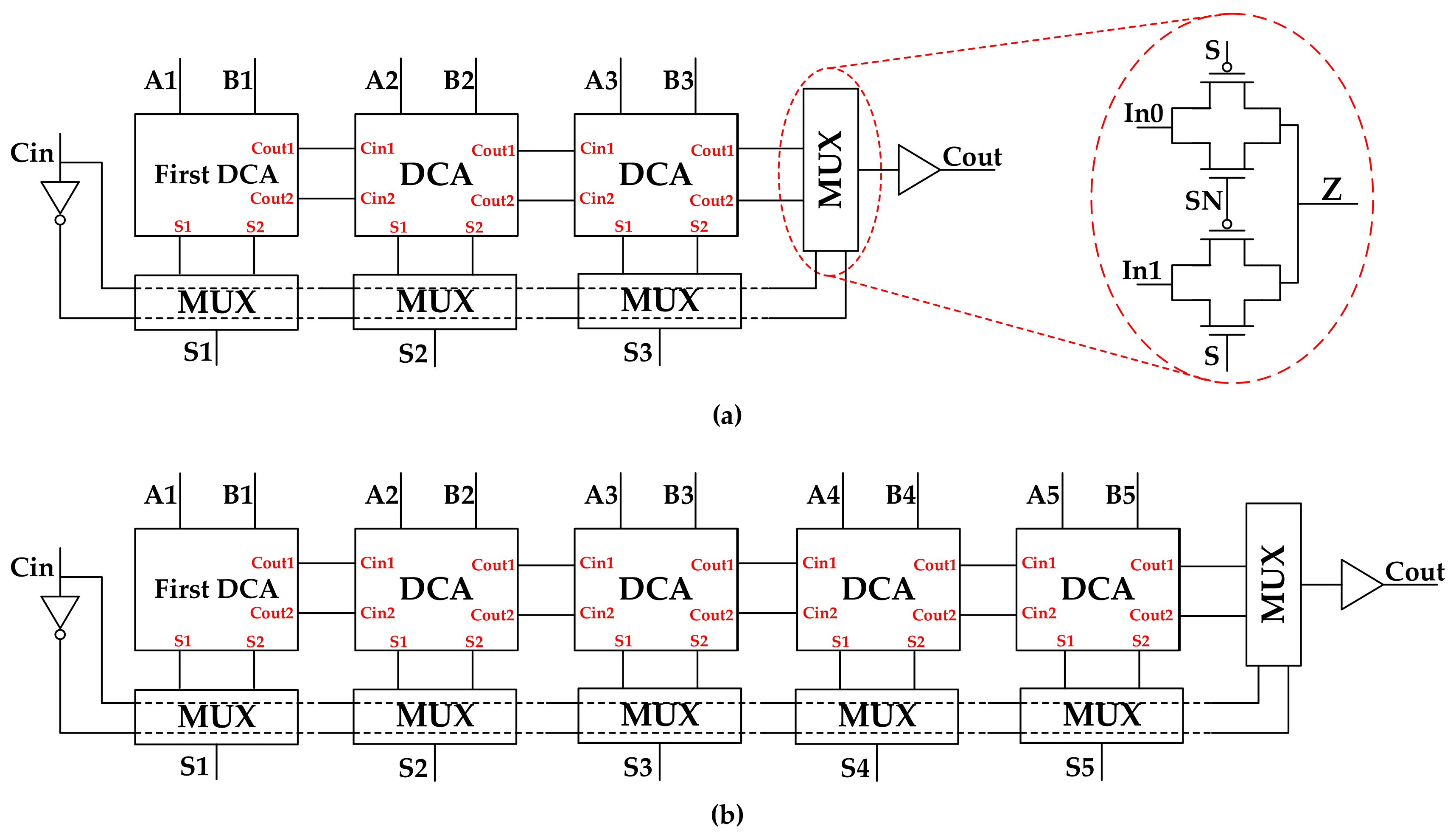
The single-stage CSLA with different bit widths consists of a different number of dual carry adders, while the correct sum and carry outputs are selected through multiplexers.
Figure 3a,b show the architecture of 3 bit and 5 bit single-stage CSLAs, respectively. The carry output of the previous stage is connected to the carry input of the latter stage. The carry input can propagate to the carry output quickly due to the architecture of the dual carry adder. Only primary transmission gate delay is required for carry input to propagate to carry output in dual carry adder. The adopted multiplexer consists of two transmission gates to reduce delay and power consumption. In order to increase the drive capability of the carry output of single-stage CSLA, a buffer is added to the carry output. The buffer can also interrupt the possible long transmission gate path in multi-stage CSLA, since excessive long transmission gate chain can lead to a significant increase in latency.
2.3. Architecture of Multi-Stage CSLA
When single-stage CSLAs are cascaded into a multi-stage CSLA, the multipath carry propagation feature can be fully utilized in a SQRT structure. The SQRT structure balances carry propagation delay and delay of single-stage CSLA operation by gradually increasing the bit width of the cascaded single-stage CSLAs. The SQRT structure is applied to the proposed CSLA, and
Figure 4 shows the architecture of a 16 bit CSLA which is composed of several proposed single-stage CSLAs. Similar to regular SQRT CSLA, the proposed CSLA divides the addition into sub-addition with different bit widths, and the bit widths of sub-addition increase by one progressively to balance carry propagation delay and delay of single-stage CSLA operation. For single-stage CSLA, once the bit width is increased by one, the delay is increased by one inverter delay and one transmission gate delay. For multi-stage CSLA, once the carry signal passes through a single-stage CSLA, the delay is increased by one transmission gate delay and one buffer delay. Thus, the increased by one method could balance carry propagation delay and delay of single-stage CSLA operation to a certain extent. At the same time, since the carry propagation delay is slightly larger than the delay of single-stage CSLA, the glitches of the carry signal can be reduced, and the power consumption is reduced. Eight-bit and 32 bit CSLAs are also implemented in this paper, and which are composed of 2b, 2b, 4b single-stage CSLAs and 2b, 3b, 4b, 5b, 6b, 6b, 6b single-stage CSLAs, respectively, to reduce the adder delay.
3. Simulation Results and Discussion
To verify the performance of the proposed CSLA, post-layout simulation comparisons were made among the proposed CSLA, regular SQRT CSLA, BEC-based CSLA, and the CSLA in Reference [
14]. The regular SQRT CSLA, BEC-based CSLA, and the CSLA in Reference [
14] are based on the standard cell library, as in the references [
6,
14]. The standard cell library is mainly composed of static CMOS logic. All the simulations were performed on a SMIC 55 nm process.
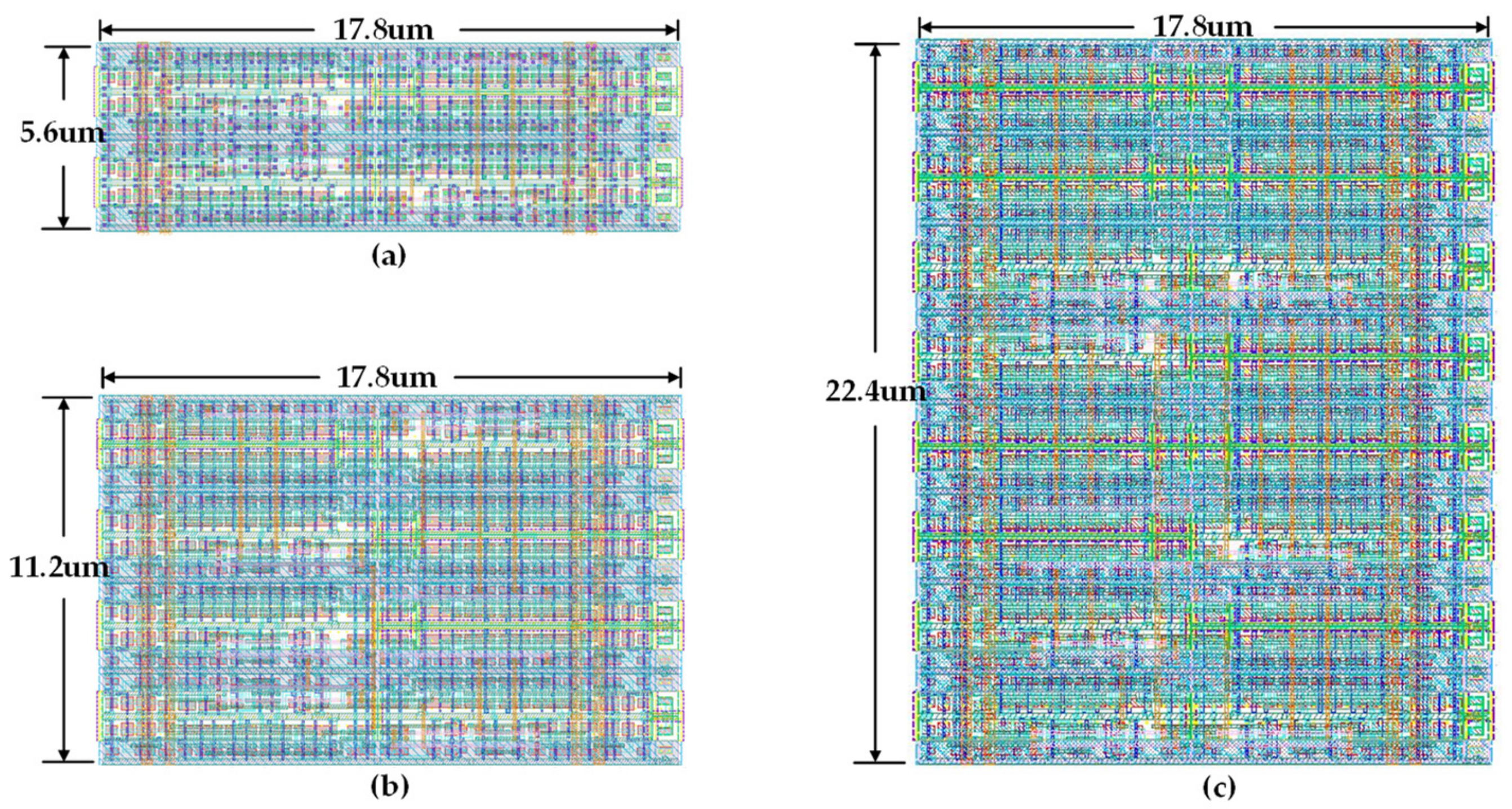
The layouts of the proposed 8 bit, 16 bit, and 32 bit CSLAs are shown in
Figure 5a–c, respectively. The layouts can achieve nearly 100% utilization due to the regular structure of the proposed CSLA. The area of the proposed 8 bit, 16 bit, and 32-bit CSLAs were as compact as 99.68 μm
2, 199.36 μm
2, and 398.72 μm
2, respectively. Actually, the average area of each bit of the proposed CSLAs with different widths was the same, 12.46 μm
2.
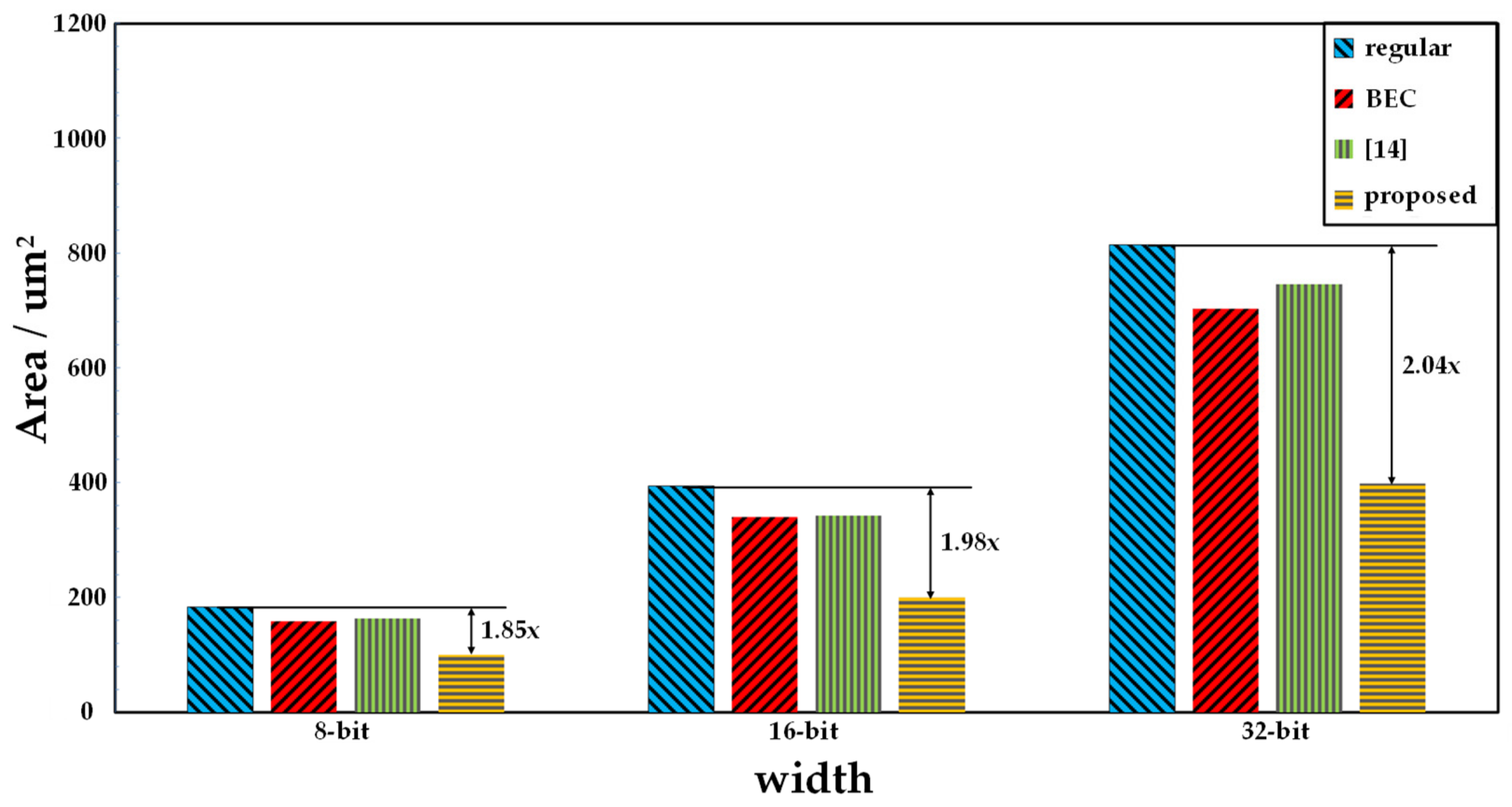
Figure 6 shows the area comparison among the four types of CSLAs. As shown, the regular CSLA had the largest area due to the excessive redundant structure. The BEC-based CSLA and the CSLA in Reference [
14] used several methods to optimize the logic of the CSLAs, and the areas were somewhat lower than that of the regular CSLA. In this paper, with the employment of the proposed dual carry adder, the transistors required for addition were greatly reduced. At the same time, hybrid logic was adopted to reduce the overhead of the logic operation as much as possible. Thus, the area of the proposed CSLA was greatly optimized using the improved structure of the adder. The area of the proposed CSLA was reduced by nearly half compared with that of the regular CSLA as shown in
Figure 6.
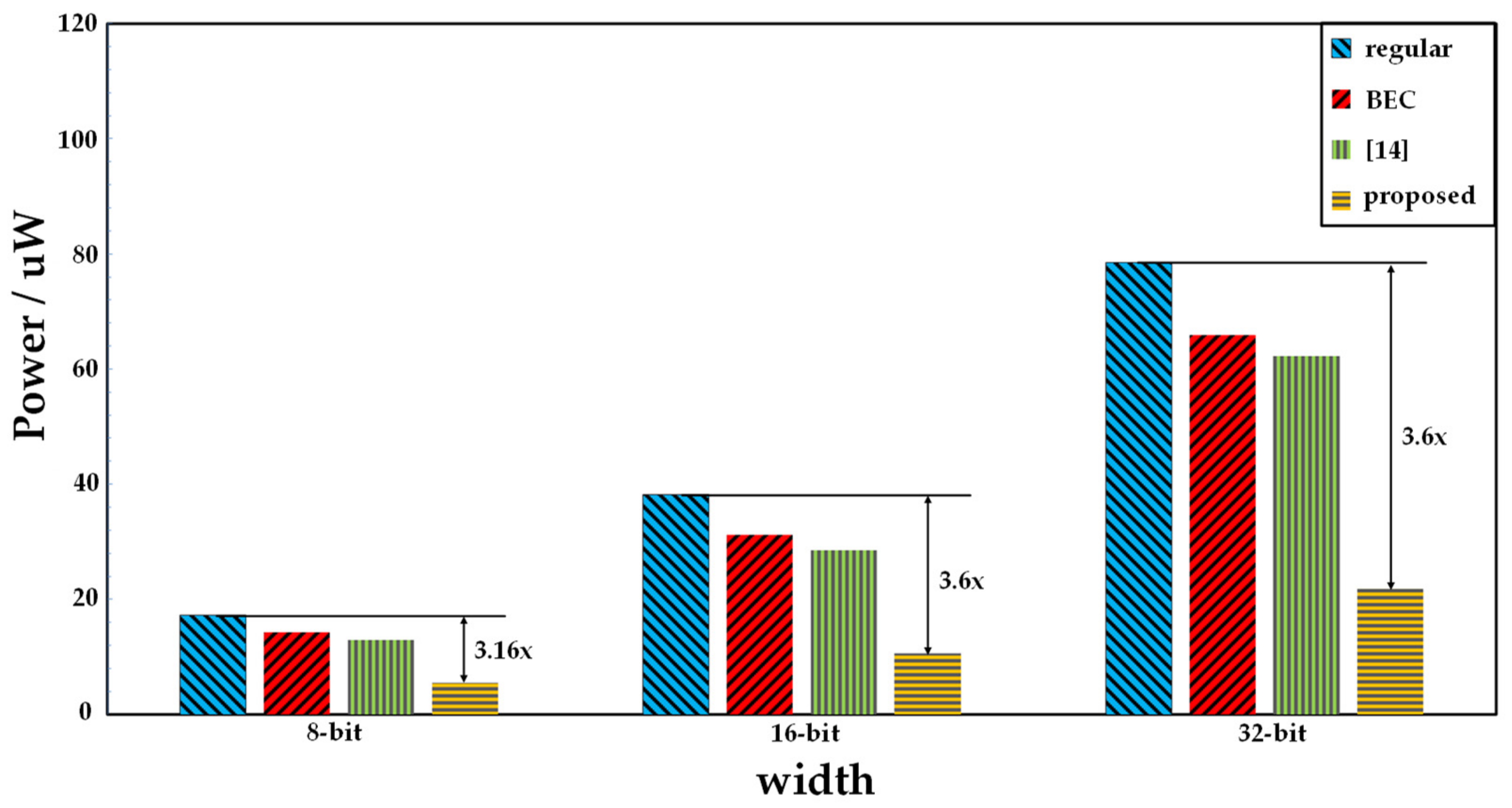
In order to verify the effectiveness of the proposed CSLA in reducing power consumption, benchmarks composed of 1000 pairs of random numbers were applied to the three types of CSLAs. Synopsys FineSim was employed to run the power consumption simulation. The simulation was performed at a speed of 100 M additions per second. Typical PMOS and typical NMOS were employed with a supply voltage of 1.2 V. Similar to the area comparison, the regular CSLA had the largest power consumption, as shown in
Figure 7. The BEC-based CSLA and the CSLA in Reference [
14] reduced some logic overhead compared with the regular CSLA, and the power consumption was slightly reduced. In this paper, the proposed dual carry adder reused as much logic as possible. Furthermore, the proposed dual carry adder mostly used transmission gate logic to minimize the power consumption. As shown in
Figure 7, the power usage of the proposed CSLA was reduced by up to 72.2% compared with that of regular CSLA.
Fully custom CSLA cannot directly obtain the maximum delay of the circuit through the static timing analysis tool. It is also impossible for the large bit width full adder to traverse all possible inputs to obtain the maximum delay. Therefore, it is necessary to analyze the critical path of the circuit and give the excitation corresponding to the critical path to obtain the delay of the circuit. For the proposed CSLA, there are two critical paths that need to be considered. One is the carry propagation path through all single-level CSLAs, and the other is the operation latency of the last single-level CSLA, as discussed in
Section 2.3. Several pairs of excitations have been applied to the proposed CSLA to measure the delay of the CSLA.
Table 1 shows the excitations of the 16 bit CSLA, and the excitations of the 8 bit and 32 bit CSLAs were similar to those of the 16-bit. As shown in
Table 1, the first three sets of excitations were designed to test the maximum carry propagation delay while the last three sets of excitations were designed to test the maximum delay of the single-stage CSLA. In order to test the maximum carry propagation delay, the carry signal needs to propagate from the first single-stage CSLA to the last single-stage CSLA in the first three sets of excitations. Similarly, the last three excitations test the maximum delay of the single-stage CSLA since the bit width of the last single-stage CSLA in 16 bit CSLA is 5. The maximum value of the delay obtained by the different excitations is considered to be the maximum delay of the circuit. All the initial values of the excitations were set to 0. Slow NMOS, slow PMOS, a temperature of 125 °C, and 10% supply voltage drop (1.08 V) were applied to the HSPICE simulation to get the worst-case delay. The same excitations were given to the regular SQRT CSLA, BEC-based CSLA, and CSLA in Reference [
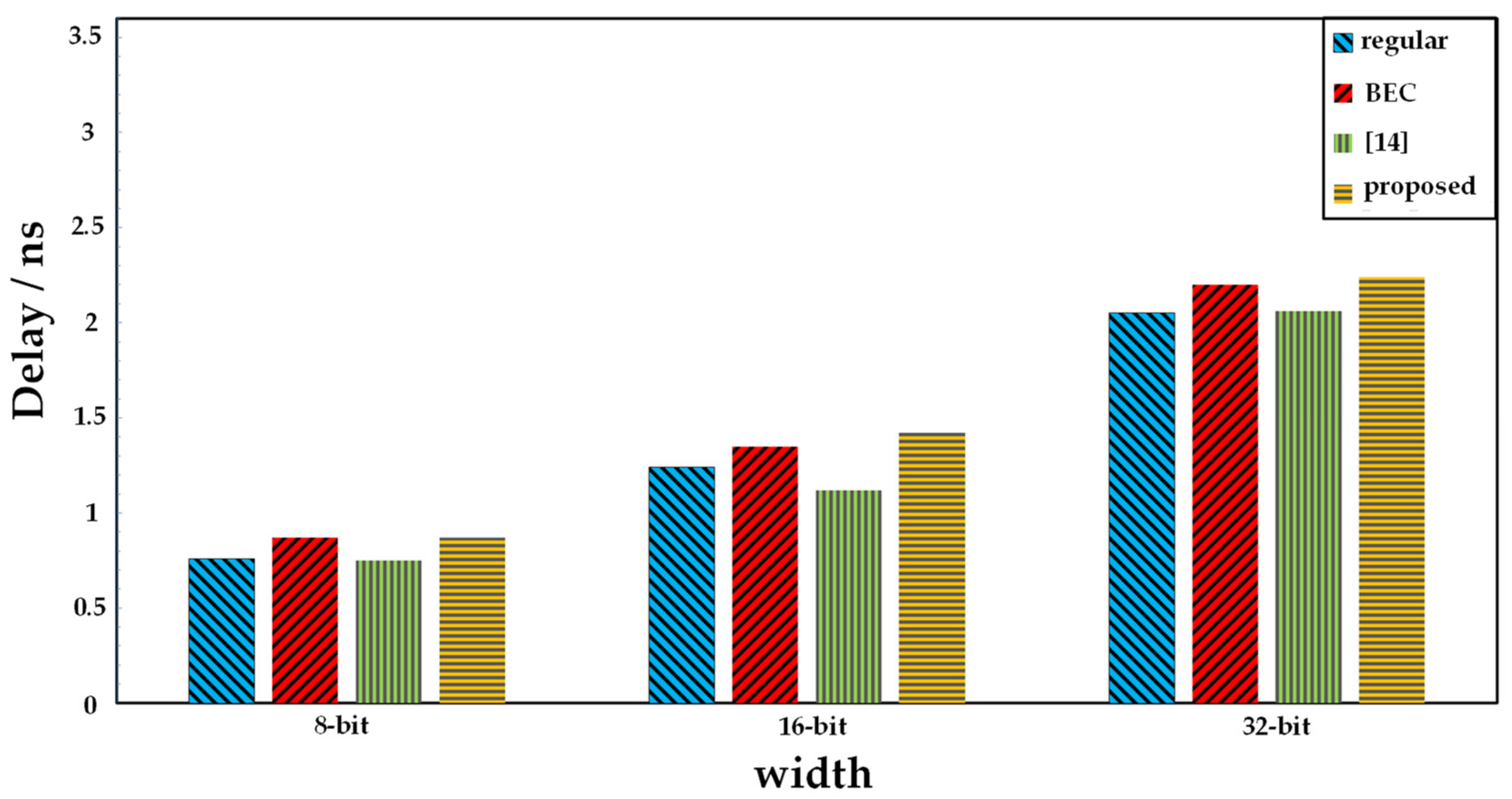
14] and their corresponding maximum delay for comparison. As shown in
Figure 8, the delay of the BEC-based CSLA was slightly larger than the regular CSLA, as described in Reference [
6]. The CSLA in Reference [
14] skips the carry computation in the first stage of each bit-slice block, and the delay was reduced compared with the BEC-based CSLA, similar to that of the regular CSLA. The delay of the proposed CSLA was similar to the BEC-based CSLA and a little larger than the regular CSLA. Since the carry propagation delay was designed to be slightly larger than the single-stage CSLA delay to reduce glitches, the delay of the proposed CSLA can be reduced by increasing the bit widths of the cascaded single-level CSLAs and reducing the cascaded stages, which may slightly increase the power consumption.
Table 2 provides a detailed comparison of the four SQRT CSLAs as well as RCA and carry look ahead adder. As shown in
Table 2, RCA had the largest delay due to the longest carry propagation path. Both the carry look ahead adder and the CSLA can significantly reduce the delay of the addition. The delay of the carry look ahead adder grows slowly with bit width increases, so the carry look ahead adder has delay advantages for large bit width addition. For medium bit width addition, such as 8 bit, the delay advantage of the CSLA was more obvious. Meanwhile, as the excitations in
Table 1 were designed to test the maximum delay of the CSLA, the results of the carry look ahead adder may not be able to represent the maximum delay. Furthermore, the area of carry look ahead adder was higher than that of the CSLA due to the complex carry generation circuit.
Among the four types of CSLAs, the proposed CSLA had the smallest power and area, which was mainly due to the proposed dual carry adder. With the architecture of the proposed dual carry adder which reused logic as much as possible, as well as the hybrid logic, the complexity of the CSLA was greatly reduced as was the power and area. As shown in
Table 2, the power of the proposed CSLA was much lower than that of other CSLAs and even lower than that of the RCA. The area of the proposed CSLA was also much lower than that of the other CSLAs, and only slightly larger than the RCA. The delay of the proposed CSLA was slightly larger than that of the regular CSLA and the CSLA in Reference [
14], which still showed significant delay advantage compared with the RCA. As described in the previous paragraph, delay of the proposed CSLA can also be optimized, which may increase power consumption. The trade-off between speed and power consumption needs to be combined with specific application scenarios. The area-power-delay product of the proposed CSLA was much smaller than other architectures, showing tremendous power and area efficiency. Thus, the proposed CSLA is the best choice to provide fast addition where area and power is limited.


