Article

Hybrid PWM Strategy for Power Efficiency Improvement of 5-Level TNPC Inverter and Current Distortion Compensation Method

Department of Electrical Engineering, Konkuk University, Seoul 05029, Korea
*
Author to whom correspondence should be addressed.
Electronics 2019, 8(1), 76; https://doi.org/10.3390/electronics8010076
Submission received: 18 November 2018 / Revised: 31 December 2018 / Accepted: 4 January 2019 / Published: 10 January 2019
(This article belongs to the Special Issue Renewable Electric Energy Systems)

Abstract

:
This paper proposes a pulse width modulation (PWM) strategy for improving the efficiency of a 5-level H-bridge T-type neutral point clamped (TNPC) inverter. In the case of the proposed PWM strategy, unlike the conventional PWM strategy in which both of the switching legs of the H-bridge inverter operate at a high frequency, one switching leg of the inverter operates at a low frequency. As the switching frequency is lowered, the switching loss is reduced, this improving the efficiency of the system. The duty references for the switching legs and the operating principle of the inverter are described in detail. The proposed PWM strategy, however, causes distortion of the output filter inductor current. The cause of the distortion has been analyzed and a compensation method is proposed to mitigate the distortion of the current. The effect of the proposed PWM strategy can be predicted through the loss calculation of the inverter for each modulation strategy. Furthermore, current distortion mitigation obtained by compensation method is confirmed through the simulation. In order to verify the effectiveness of the proposed strategy, a 2 kW H-bridge TNPC inverter prototype is implemented and tested. The simulation and experimental results show that the efficiency of the inverter is improved when the proposed PWM strategy is applied.

1. Introduction

As power consumption has increased recently, the power density of power electronic systems has become a major concern for researchers. Studies focused on efficiency improvement and reducing the volume of the system have been carried out to maximize power transfer. Most inverters used in renewable energy systems, energy storage systems (ESS), uninterruptible power supply (UPS), and solid-state transformers (SST) adopt the topology of a 2-level inverter [1,2,3,4,5,6,7]. The 3-level inverter can synthesize the output by subdividing the voltage level by one more than the 3-level inverter. Thus, the 3-level inverter has better d v / d t characteristics and total harmonic distortion (THD) performance [8,9]. Therefore, if the inverter topology is changed to a 3-level inverter, a filter size that is smaller than the output filter size of a 2-level inverter can be designed, thus reducing the size of the entire system. Examples of a 3-level inverter, such as neutral point clamped (NPC) inverter [8,10], T-type neutral point clamped (TNPC) inverter [11], and flying capacitor inverter [12] have been studied and widely used.
Another way to reduce the size of the power converter is to change the switching devices. Although Silicon (SI) -based switching devices have been used in all industries, they have been replaced by the growth of wide bandgap (WBG) semiconductor devices such as Silicon Carbide (SiC) and Gallium Nitride (GaN). Many power converters using WBG devices with different characteristics from conventional Si-based devices have been studied [13,14,15,16,17]. WBG devices have higher blocking voltage, higher switching frequency, higher thermal conductivity, and lower on-state loss than Si-based devices [14,18]. Therefore, the power density can be increased by using WBG devices.
Other studies on improving the power density of H-bridge inverters have been conducted on asymmetric inverters with different switching leg topologies [19,20,21,22]. An inverter with a switching leg in combination with a 3-level and 2-level topology has been proposed in [19,20,22]. An inverter consisting of one switching leg with NPC inverter and the other leg with TNPC inverter has been proposed in [21].
In this paper, a changed PWM strategy for power efficiency improvement of 5-level H-bridge TNPC inverter is proposed. This is contrary to the previous studies mentioned, that have proposed changes to the topology or switching devices of the inverter. By applying the proposed PWM strategy that modifies the switching frequency of switching legs without changing the hardware topology, each switching leg operates at a different frequency. One of those legs operates at the commercial frequency (60 Hz) and its switching losses can be reduced. The operation and principles of each PWM strategy are described in detail in the next section. In addition, the proposed PWM strategy causes a distortion problem in regard to the output filter of the inductor current. Therefore, a compensation method for the distortion is suggested. By using the compensation method, the inductor current distortion near the zero crossing can be effectively compensated. Moreover, the loss calculation method, based on the datasheet of the switching device described in [23], is applied to the simulation model to compare the losses of the inverter for each PWM strategy. The simulation and experimental results show that the efficiency of the 5-level H-bridge TNPC inverter is improved by applying the proposed PWM strategy.

2. PWM Strategy for 5-LEVEL H-Bridge TNPC Inverter

2.1. TNPC Inverter Configuration and the Conventional PWM Strategy

Figure 1 shows the topology of 5-level H-bridge TNPC inverter. The inverter consists of two dc-link capacitors and two switching legs. One switching leg consists of four switching devices, which are chosen to be Si insulated gate bipolar transistor (IGBT) devices. Table 1 summarizes all the variables used in this paper. Each switching leg synthesizes the pole voltage v a n or v b n using three voltage levels, V d c / 2 , 0 and V d c / 2 , with respect to the voltage reference shown in Figure 2. With the pole voltage level combination of the two phase switching legs, the output voltage v A B has five voltage levels V d c , V d c / 2 , 0, V d c / 2 and V d c .
Table 2 shows voltage levels of the output voltage v A B according to the polarity of the voltage and switching function S when the inverter operates on the voltage reference with the conventional PWM strategy. There are eight states form A-1 to A-8, and the output voltage has zero voltage level with the same switching function at A-1 and A-5. In A-2 and A-3, the inverter output the same voltage level V d c / 2 although the switching functions are different. Both states occur when the inverter operates with unipolar PWM. Even when the polarity of the output voltage is negative, the inverter output the same voltage level V d c / 2 in A-6 and A-7. Figure 3 represents the current flow path for the eight states in Table 2. When the polarity of the voltage reference is positive, S 1 and S 3 of the switching leg A operate complementarily, S 6 and S 8 of the switching leg B are also complementarily switched. Conversely, when the polarity of the reference is negative, S 2 and S 4 of the switching leg A operate complementarily. Similarly, S 5 and S 7 of the switching leg B operate in the same manner. Therefore, the duty reference of the switch pairs based on the upper switch and the lower switch can be easily obtained by using a limiter. The duty reference for each pair can be seen in Figure 4. The conventional PWM strategy operates with sinusoidal pulse width modulation (SPWM).

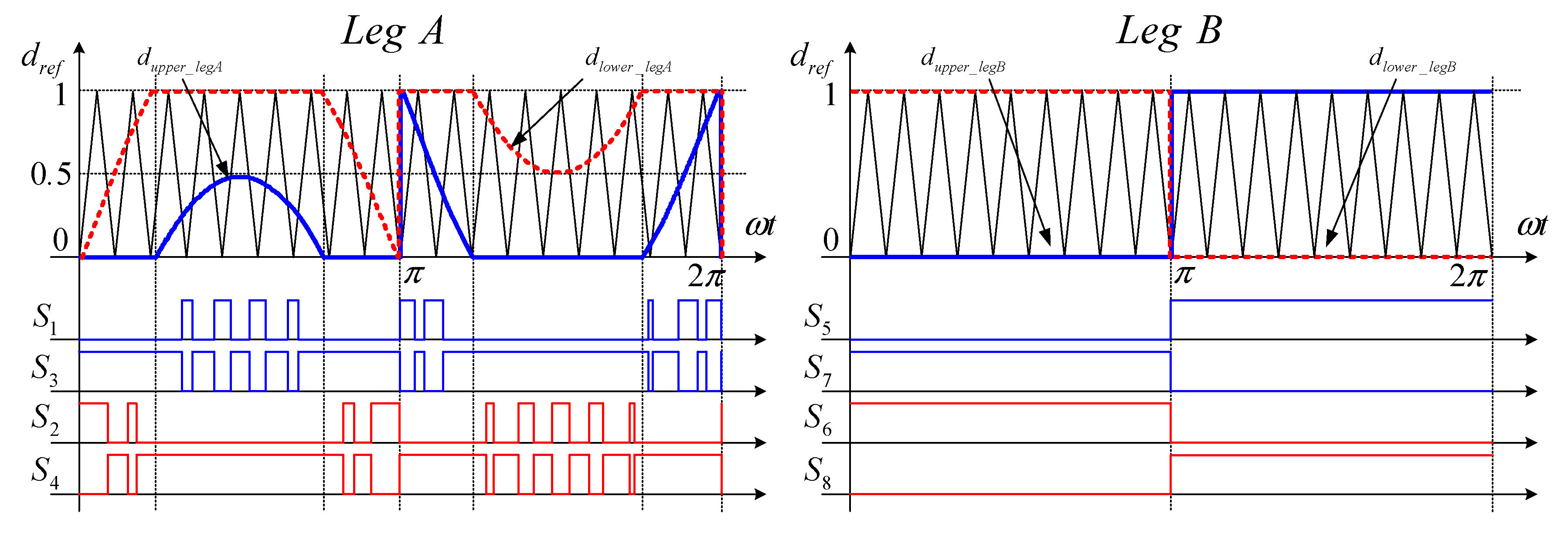
2.2. The Proposed PWM Strategy and Compensation Method

In the proposed PWM strategy, which is different from the conventional PWM strategy, one of the two switching legs operates at 60 Hz, the same as the voltage reference frequency. The other switching leg operates at a switching frequency generally more than 10 kHz. Therefore, the switching function must be changed to synthesize the same voltage in the proposed PWM strategy.
Table 3 summarizes the output voltage according to the polarity and switching function in the proposed PWM strategy. There are six states from B-1 to B-6 and the switching function of switching leg B changes according to the polarity of the output voltage, therefore operating with the voltage reference frequency. If the modulator is the same as the conventional strategy, i.e., the upper or lower switch and the neutral switch are complementary, the duty reference must be modified differently from the conventional one. Based on the summary in Table 3, the current flow path for each state is shown in Figure 5.
The switching function of the states shown in Table 2 can be used to determine the switch operating in six intervals divided by the modulation index (MI) of the voltage reference in Figure 2. If the polarity of the output voltage is positive, switching devices S 5 , S 8 of switching leg B are off and S 6 , S 7 are on. Conversely, when the polarity is negative, the devices S 5 and S 8 are on, and S 6 , S 7 are off. First, state B-1 and B-2 appear alternately in the interval 1 and the interval 3 in which MI is in the range of 0 < m < 0.5 , the output voltage is in a range of 0 < v o u t < V d c / 2 . The devices operating in switching leg A are S 2 and S 4 . Second, state B-2 and B-3 appear alternately in the interval 2 where MI is 0.5 < m < 1 , the output voltage synthesizes the voltage in the range of V d c / 2 < v o u t < V d c . The switches S 1 and S 3 operate in this interval. Third, since the state B-4 and state B-5 are alternated in the interval 4 and interval 6 where MI is 0.5 < m < 0 , and the output voltage has a range of V d c / 2 < v o u t < 0 . The switches S 1 and S 3 operate in those intervals. Finally, in interval 5 where MI is 1 < m < 0.5 , state B-5 and B-6 are alternated and the output voltage range is V d c < v o u t < V d c / 2 . The devices S 2 and S 4 turn on and off in this interval. In order to synthesize the output voltage according to the above-mentioned voltage reference, the upper and the lower switch duty reference of each switching leg should be modified as shown in Figure 6.
In the proposed PWM strategy, the operating frequency of the switching leg B is significantly lower than that of the conventional PWM strategy as can be seen from the switching signals according to the duty reference in Figure 6. Therefore, the proposed PWM strategy has the advantage of reducing the switching losses and improving the efficiency. However, the proposed strategy suffers from filter inductor current distortion near the zero crossing. This distortion is caused by the output voltage generated in the form of a pulse that deviates from the voltage reference by the PWM setting and PWM update time of the digital controller. In the case of the conventional PWM strategy, the state A-1 and state A-5, in which the output voltage is zero voltage, have the same switching function even if the polarity of the output voltage is different. And the duty ratio of the upper or lower switch is decreased and the duty ratio of the neutral switch is increased as the voltage reference becomes closer to the zero voltage where the polarity changes. But the switching functions of state B-1 and B-4, in which the output voltage is the zero voltage, are different from each other. Since the switching function for zero voltage is different, the duty ration of the switching leg A’s neutral switch is increased as the voltage reference gets closer to the zero voltage. But the switching leg B does not exhibit such a tendency. Therefore, the output voltage becomes V d c / 2 or V d c / 2 instead of zero voltage due to the state of the switching leg A before the duty ratio of the switching leg B changes. A solution to this problem is to apply both the proposed PWM strategy and the conventional PWM strategy as a mixed method. This compensation method adopts the conventional PWM strategy when a phase ϕ of the voltage reference is in the range α < ϕ < α for a small phase α that can cover the PWM update time of the switching leg B. In other ranges, the proposed PWM strategy is applied. It is possible to compensate for the current distortion near the zero crossing by preventing the generation of erroneous output voltage with the conventional PWM strategy, and to improve the efficiency by applying the proposed PWM strategy in the remaining phases.

3. Simulation Results

The 5-level H-bridge TNPC inverter shown in Figure 1 was implemented in PSIM 11.1.3 from Powersim corporation to compare operations for each PWM strategy. Table 4 gives the parameters used in the simulations. The reason why the switching frequency of Table 4 is different between the conventional PWM strategy and the proposed PWM strategy is that the ripple condition of the filter current is the same. If the switching frequency is 20 kHz in the conventional PWM strategy, the effective switching frequency becomes 40 kHz by unipolar PWM switching. Therefore, in order to achieve the same current performance in the proposed PWM strategy, the switching frequency should be set to 40 kHz which is twice the conventional PWM strategy. Figure 7 shows the waveforms when the inverter operated with the conventional PWM strategy in the simulation. Figure 7b shows the upper and lower duty reference of switching leg A which was made up of the voltage reference v r e f in Figure 7a. Using the limiter in the voltage reference, it can be confirmed that each wave form was made. Figure 7c,d show the output voltage v A B of the inverter operating with those duty references and output filter inductor current i L f . It can be seen that the output voltage v A B had 5-level voltages as analyzed in Table 2. The inductor current was output at the frequency of the voltage reference and was in phase with the output voltage.
Figure 8 shows the waveforms when the inverter operated with the proposed PWM strategy. Figure 8a represents the voltage reference v r e f same as Figure 7a. And Figure 8b shows the upper and lower duty reference of the proposed PWM strategy which can be obtained by the voltage reference. As described in the previous section, it can be seen that the upper and lower duty reference were modified for each interval divided by the MI of the voltage reference. Figure 8c,d show the output voltage and the inductor current when the inverter operated using the proposed PWM strategy. It can be confirmed that the output voltage had 5-level voltages, the same as the conventional PWM strategy, but the inductor current had the problem mentioned above. There was a distortion due to the incorrect output voltage. When the inverter was operated with the proposed PWM strategy using the compensation method, the inductor current waveform, as shown in Figure 9, was obtained. In Figure 9, it can be seen that the application of the compensation method had the effect of alleviating the previous current waveform distortion.
The calculation method described in [23] was simplified for the operation simulation model of Power SIM, and the power losses according to each PWM strategy were compared by adding the loss calculation block of the switching devices. Before adding the block, the V F I C E curve, which is needed for conduction loss calculation, and the E o n & E o f f I C E curves, which are needed for the switching loss, calculations should be form the datasheet of Infineon’s IRGB4062DPbf IGBT and applied to the actual hardware in the experiment. Following this, the approximation for each curve by using MATLAB should then then proceed. Figure 10a,b show the V F I C E curves of the IGBT and the parallel diode taken from the datasheet. The conduction loss P c o n d _ I G B T of the IGBT, the diode conduction loss P c o n d _ d i o d e curve and the second order approximation curves derived by the curve fitting, respectively, are shown in Figure 10c,d. The E o n I C E curve taken from the datasheet was approximated using the curve fitting to obtain the switching losses. The E o f f I C E curve was also approximated by the same method, and those curves and the curves of the datasheet are shown in Figure 11a,b respectively.
In the simulation, it was possible to calculate the conduction loss and the switching loss occurring during the operation of the inverter by substituting the information of the current flowing through each switching device and switching signals into the approximation curves. Figure 12 shows the upper and lower switch conduction losses and switching losses of switching leg B when the inverter operated at a rated power of 2 kW. Figure 12a,b show the losses when applying the conventional PWM strategy and the proposed PWM strategy. Comparing Figure 12a,b, the conduction loss of the switching leg B was slightly increased but the switching loss was greatly reduced when the proposed PWM strategy was applied.
Simulation efficiency curves were obtained by calculating the losses of all switches of inverter at changing load. The efficiency curves drawn by changing the load condition from 250 W to 2 kW in 250 W increments is shown in Figure 13. When the proposed PWM strategy was applied, the efficiency of the inverter was improved over the entire load conditions as compared with the conventional PWM strategy. As a result of the simulation, the proposed PWM strategy may cause a slight distortion in the inductor current. But it can be expected to improve the power density because of its higher efficiency.

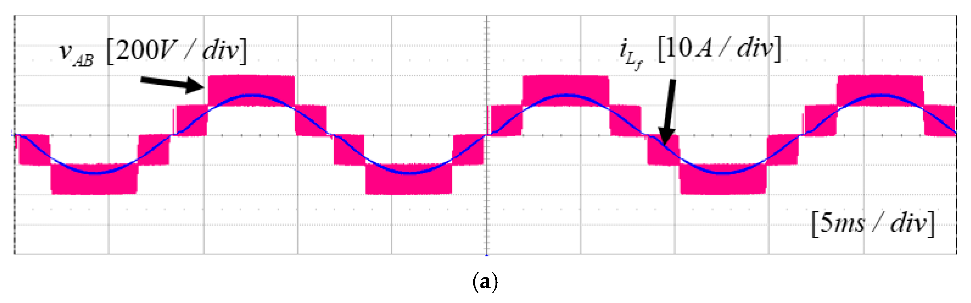
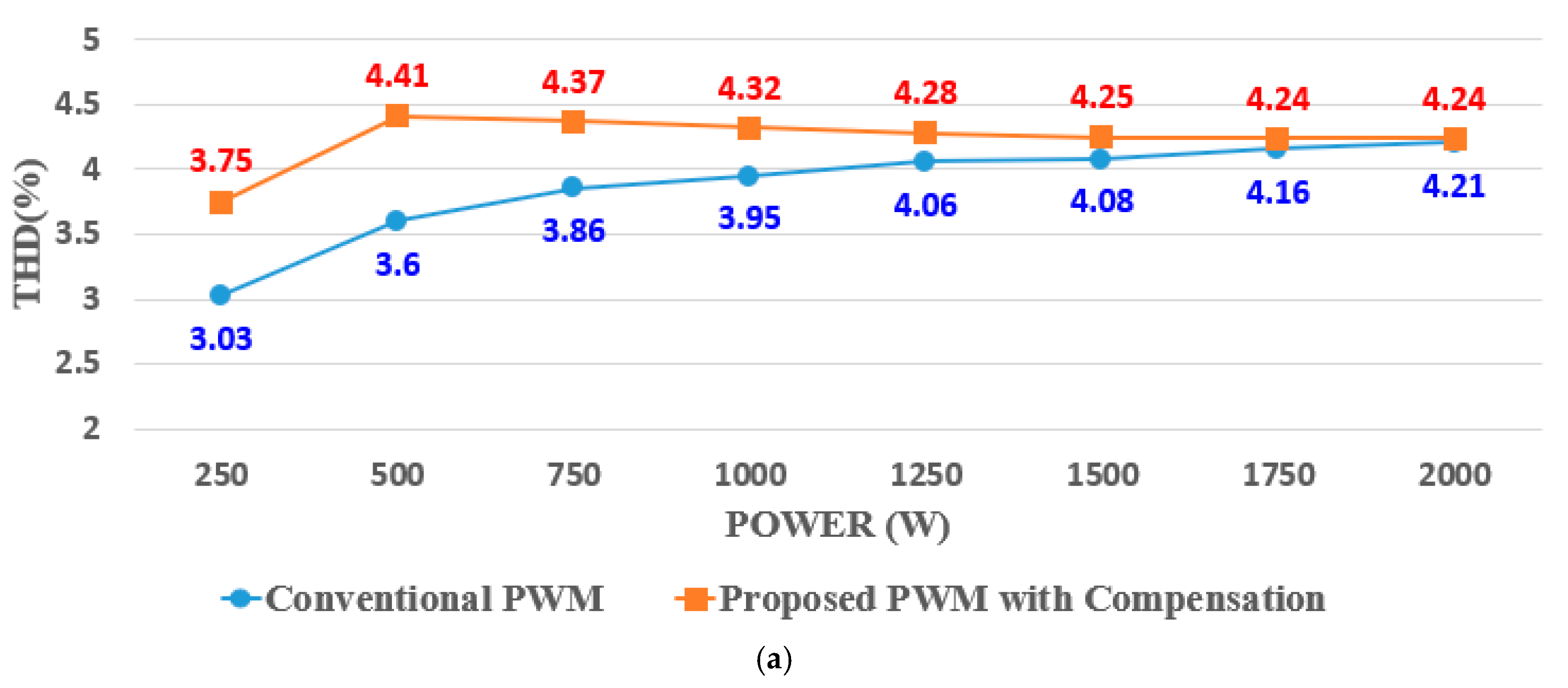
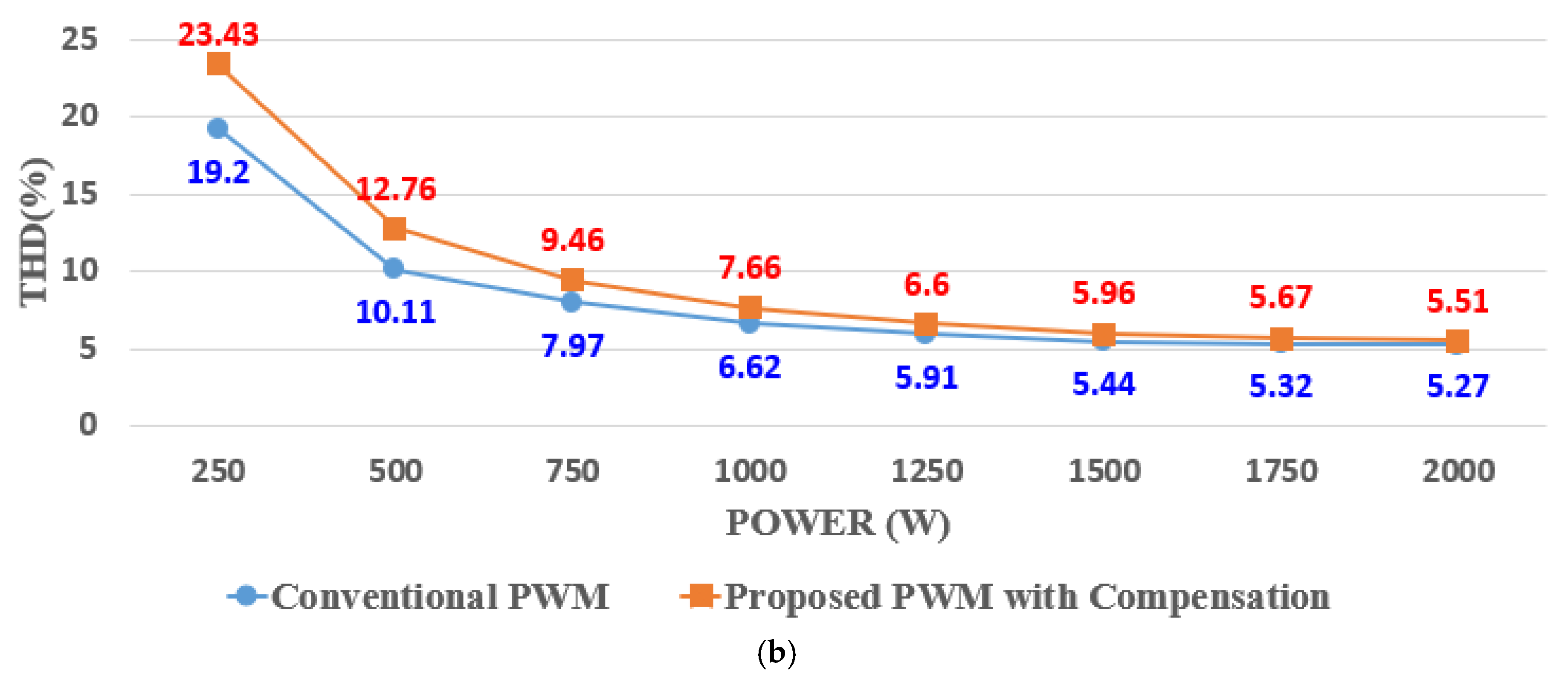
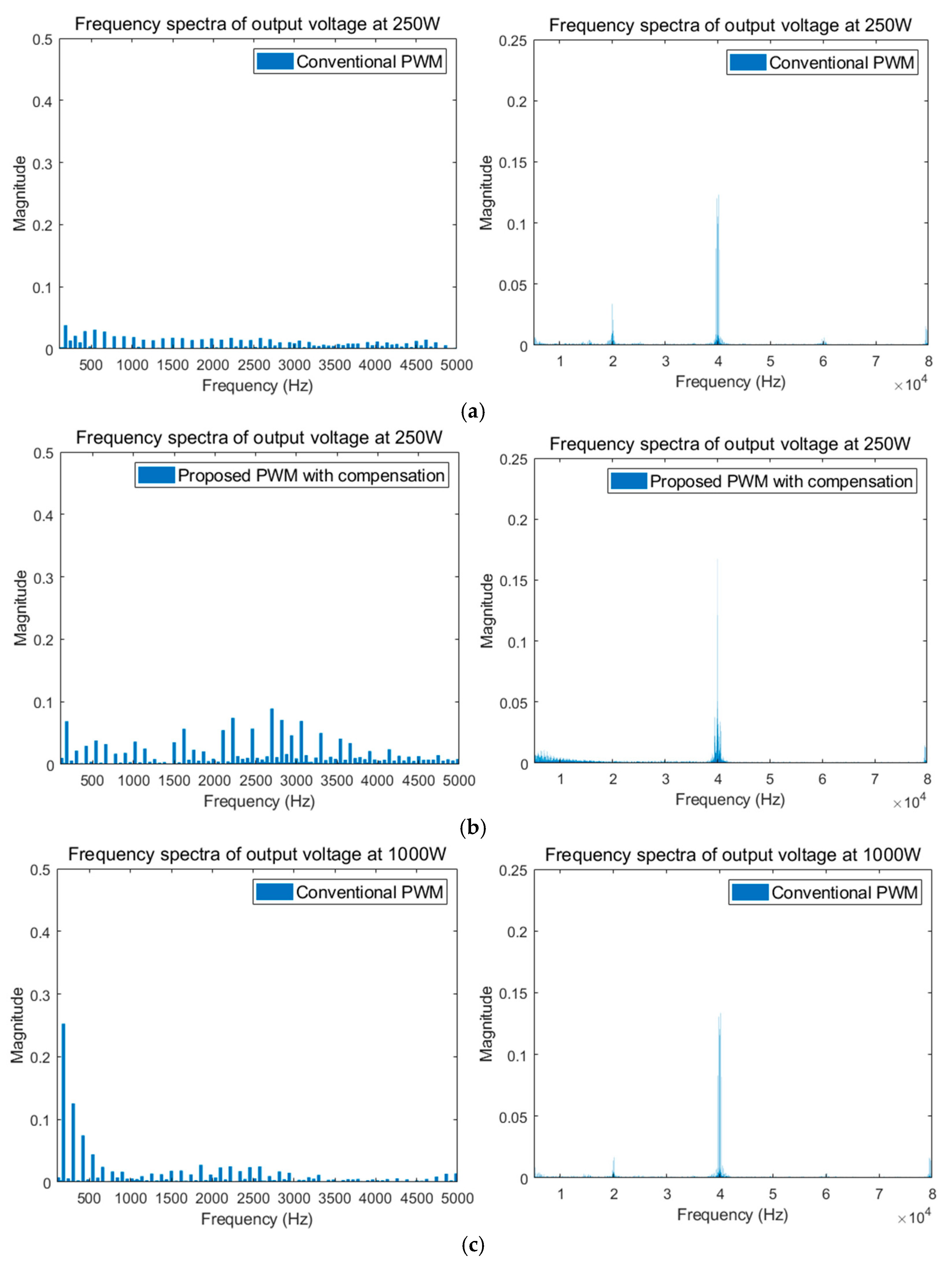
4. Experimental Results

The 5-level H-bridge TNPC inverter prototype for verifying the effect of the proposed PWM strategy analyzed above is shown in Figure 14. The prototype consisted of a digital control board, a power stage consisting of two half bridge TNPC inverter modules, a PWM interface board, and an output LC filter. This prototype is set as shown in Figure 15, and the Chroma’s electronic load 63804 was connected in the power stage for AC load. The efficiency was measured with open loop voltage control without any feedback control. The specification of the prototype for the experiment was the same as that of the simulation summarized in Table 4.
Figure 16 shows the output voltage v A B and the output filter inductor current of 5-level H-bridge TNPC inverter with each PWM strategy at a rated power of 2 kW. Comparing Figure 16a,b, output voltage had 5-level voltages both PWM strategies but the spike type distortion in inductor current occurred near the zero crossing when the inverter operated with the proposed PWM strategy. In Figure 16c, the distortion of the inductor current was mitigated by applying the compensation method described in the previous section.
The THD of the output voltage and of the inductor current were measured to compare the output quality of the inverter operating with each PWM strategy. The THD curves of the output voltage and the inductor current are shown in Figure 17. The THD of the output voltage tended to increase gradually as the load increased, and the THD of the inductor current decreased as the load increased. However, the THD differences, when operating with each PWM strategy, were large at the light load conditions, and the differences were small when operating at the rated power condition. In the rated power condition, the differences of THD had a value within the error range, and it can be seen that the inverter outputs almost the same voltage and current quality regardless of the PWM strategy. The frequency spectra of the output voltage and the inductor current with the low frequency harmonics up to 5 kHz and with the high frequency harmonics up to 80 kHz are shown in Figure 18 and Figure 19. The frequency spectra were analyzed under three power conditions: 250 W, 1000 W, and 2000 W. The frequency spectra of the output voltage and the inductor current in Figure 17 and Figure 18 show more harmonic components in the low frequency harmonic components when the proposed hybrid PWM strategy was applied. However, there was no significant difference from the conventional PWM strategy in the high frequency harmonic components. As the power condition changed from the light load to the rated load, the harmonic component characteristics tended to be similar regardless of the PWM strategy employed.
The efficiency of 5-level H-bridge TNPC inverter when it operated with open loop control was measured by using Yokogawa’s power analyzer WT1800. Figure 20 shows the efficiency curves of the inverters according to each PWM strategy at the same load condition as in the simulation performed. It can be recognized that the efficiency of the proposed PWM strategy was higher than that of the conventional PWM strategy over the entire load conditions. The highest efficiency was 98.12% at 750 W power condition. The difference between the efficiency of the proposed PWM strategy and the efficiency of the conventional PWM strategy was large in the light load region. It became smaller as the load condition was heavier. This tendency was due to the fact that the main effect of the proposed PWM strategy was to improve the efficiency by reducing the switching loss, so that the effect becomes more significant in the light load region where the switching loss is dominant. It can be seen that the proposed PWM strategy improved the efficiency of the inverter from 0.39% to 2.17% compared to the conventional PWM strategy. Compared with the application of the method for compensating the inductor current distortion near the zero crossing to the proposed PWM strategy, the efficiency was slightly improved in the light load condition. In the other load condition, similar efficiency results were obtained regardless of whether or not the compensation method was applied. Through Figure 16 and Figure 20, it can be verified that the simulation results performed in the earlier section are well matched with the experimental results.

5. Conclusions

This paper proposes a PWM strategy for improving the efficiency of a 5-level H-bridge TNPC inverter. The output voltage states, the current flow path, duty reference, and operating principle for the conventional PWM strategy and the proposed PWM strategy were compared. This explains how the proposed PWM strategy can improve the efficiency of the system. In addition, when the proposed PWM strategy was applied, distortion occurred in the output filter inductor current of the inverter. However, a compensation method for mitigating this distortion was also proposed. The proposed PWM strategy improved the efficiency by reducing a switching loss of the switching leg. The efficiency improvement effect of the proposed PWM strategy was predicted by the loss calculation simulation. Furthermore, a 2 kW 5-level H-bridge TNPC inverter prototype was implemented to confirm the simulation results through experimentation. From the results of 250 W to 2 kW of inverter experiment, it can be confirmed that the efficiency of the proposed PWM strategy was improved from 0.39% to 2.17% than that of the conventional PWM strategy. Moreover, it can be confirmed that the current distortion in the application of the modulation strategy was mitigated by the compensation method.

Author Contributions

Conceptualization, T.L. and Y.C.; investigation, H.B.; writing—original draft preparation, T.L.; writing—review and editing, T.L.; supervision, Y.C.; project administration, Y.C.

Funding

This work was supported by “Human Resources Program in Energy Technology” of the Korea Institute of Energy Technology Evaluation and Planning (KETEP), granted financial resource from the Ministry of Trade, Industry & Energy, Republic of Korea. (No. 20174030201660). This work was supported by the National Research Foundation of Korea (NRF) grant funded by the Korea government (MSIT). (No. 2017R1C1B2009425).

Conflicts of Interest

The authors declare no conflict of interest.

References

  1. Okamoto, T.; Ishida, Y.; Kato, Y.; Miyazaki, S. Development of low voltage 2 level IGBT inverter and converter for industrial applications. In Proceedings of the 8th International Conference on Power Electronics—ECCE Asia, Jeju, Korea, 30 May–3 June 2011; pp. 2466–2473. [Google Scholar]
  2. Luo, C.; Wang, X.; Jiang, T.; Feng, R.; Xin, H.; Li, H. Experimental study of a SiC MOSFET based single phase inverter in UPS applications. In Proceedings of the 2016 IEEE Energy Conversion Congress and Exposition (ECCE), Milwaukee, WI, USA, 18–22 September 2016; pp. 1–6. [Google Scholar]
  3. Wang, R.; Wang, F.; Boroyevich, D.; Burgos, R.; Lai, R.; Ning, P.; Rajashekara, K. A High Power Density Single-Phase PWM Rectifier with Active Ripple Energy Storage. IEEE Trans. Power Electron. 2011, 26, 1430–1443. [Google Scholar] [CrossRef]
  4. Golestan, S.; Monfared, M.; Freijedo, F.D.; Guerrero, J.M. Design and Tuning of a Modified Power-Based PLL for Single-Phase Grid-Connected Power Conditioning Systems. IEEE Trans. Power Electron. 2012, 27, 3639–3650. [Google Scholar] [CrossRef] [Green Version]
  5. Bojoi, R.I.; Limongi, L.R.; Roiu, D.; Tenconi, A. Enhanced Power Quality Control Strategy for Single-Phase Inverters in Distributed Generation Systems. IEEE Trans. Power Electron. 2011, 26, 798–806. [Google Scholar] [CrossRef]
  6. Dasgupta, S.; Sahoo, S.K.; Panda, S.K. Single-Phase Inverter Control Techniques for Interfacing Renewable Energy Sources with Microgrid—Part I: Parallel-Connected Inverter Topology with Active and Reactive Power Flow Control Along with Grid Current Shaping. IEEE Trans. Power Electron. 2011, 26, 717–731. [Google Scholar] [CrossRef]
  7. Dasgupta, S.; Sahoo, S.K.; Panda, S.K.; Amaratunga, G.A.J. Single-Phase Inverter-Control Techniques for Interfacing Renewable Energy Sources with Microgrid—Part II: Series-Connected Inverter Topology to Mitigate Voltage-Related Problems Along with Active Power Flow Control. IEEE Trans. Power Electron. 2011, 26, 732–746. [Google Scholar] [CrossRef]
  8. Nabae, A.; Takahashi, I.; Akagi, H. A New Neutral-Point-Clamped PWM Inverter. IEEE Trans. Ind. Appl. 1981, IA-17, 518–523. [Google Scholar] [CrossRef]
  9. Ahmed, M.; Mekhilef, S. A three-phase three-level voltage source inverter with a three-phase two-level inverter as a main circuit. In Proceedings of the 2008 4th IET Conference on Power Electronics, Machines and Drives, York, UK, 2–4 April 2008; pp. 640–644. [Google Scholar]
  10. Hinga, P.K.; Ohnishi, T.; Suzuki, T. A new PWM inverter for photovoltaic power generation system. In Proceedings of the 1994 Power Electronics Specialist Conference (PESC’94), Taipei, Taiwan, 20–25 June 1994; Volume 391, pp. 391–395. [Google Scholar]
  11. Schweizer, M.; Kolar, J.W. Design and Implementation of a Highly Efficient Three-Level T-Type Converter for Low-Voltage Applications. IEEE Trans. Power Electron. 2013, 28, 899–907. [Google Scholar] [CrossRef]
  12. Dodo, Y.; Sato, Y.; Ito, T.; Mochidate, S. A study for improvement in power density of flying capacitor multilevel inverters for grid-connected applications. In Proceedings of the 2016 IEEE 8th International Power Electronics and Motion Control Conference (IPEMC-ECCE Asia), Hefei, China, 22–26 May 2016; pp. 469–473. [Google Scholar]
  13. Ji, S.; Reusch, D.; Lee, F.C. High-Frequency High Power Density 3-D Integrated Gallium-Nitride-Based Point of Load Module Design. IEEE Trans. Power Electron. 2013, 28, 4216–4226. [Google Scholar] [CrossRef]
  14. Kotecha, R.M.; Zhang, Y.; Rashid, A.; Vrotsos, T.; Mantooth, H.A. A physics-based compact device model for GaN HEMT power devices. In Proceedings of the 2016 IEEE 4th Workshop on Wide Bandgap Power Devices and Applications (WiPDA), Fayetteville, AR, USA, 7–9 November 2016; pp. 108–113. [Google Scholar]
  15. Zhang, Z.; Wang, F.; Tolbert, L.M.; Blalock, B.J.; Costinett, D. Understanding the limitations and impact factors of wide bandgap devices’ high switching-speed capability in a voltage source converter. In Proceedings of the 2014 IEEE Workshop on Wide Bandgap Power Devices and Applications, Knoxville, TN, USA, 13–15 October 2014; pp. 7–12. [Google Scholar]
  16. Millán, J.; Godignon, P.; Perpiñà, X.; Pérez-Tomás, A.; Rebollo, J. A Survey of Wide Bandgap Power Semiconductor Devices. IEEE Trans. Power Electron. 2014, 29, 2155–2163. [Google Scholar] [CrossRef]
  17. Wang, F.F.; Zhang, Z. Overview of silicon carbide technology: Device, converter, system, and application. CPSS Trans. Power Electron. Appl. 2016, 1, 13–32. [Google Scholar] [CrossRef]
  18. Funaki, T.; Sasagawa, M.; Nakamura, T. Multi-chip SiC DMOSFET half-bridge power module for high temperature operation. In Proceedings of the 2012 Twenty-Seventh Annual IEEE Applied Power Electronics Conference and Exposition (APEC), Orlando, FL, USA, 5–9 February 2012; pp. 2525–2529. [Google Scholar]
  19. Agelidis, V.G.; Baker, D.M.; Lawrance, W.B.; Nayar, C.V. A multilevel PWM inverter topology for photovoltaic applications. In Proceedings of the IEEE International Symposium on Industrial Electronics (ISIE’97), Guimaraes, Portugal, 7–11 July 1997; Volume 582, pp. 589–594. [Google Scholar]
  20. Valderrama, G.E.; Guzman, G.V.; Pool-Mazún, E.I.; Martinez-Rodriguez, P.R.; Lopez-Sanchez, M.J.; Zuñiga, J.M.S. A Single-Phase Asymmetrical T-Type Five-Level Transformerless PV Inverter. IEEE J. Emerg. Sel. Top. Power Electron. 2018, 6, 140–150. [Google Scholar] [CrossRef]
  21. Liu, L. Mixed single-phase three-level NPC inverter with hybrid modulation technology. In Proceedings of the 2017 IEEE Energy Conversion Congress and Exposition (ECCE), Cincinnati, OH, USA, 1–5 October 2017; pp. 2873–2880. [Google Scholar]
  22. Yang, J.H.; Le, T.V.; Ibadullaev, A.; Park, S.J. A study of TNPC type single-phase 5-level inverter for energy storage system. In Proceedings of the 2016 IEEE Transportation Electrification Conference and Expo, Asia-Pacific (ITEC Asia-Pacific), Busan, Korea, 1–4 June 2016; pp. 346–350. [Google Scholar]
  23. Drofenik, U.; Kolar, J.W. A general scheme for calculating switching-and conduction-losses of power semiconductors in numerical circuit simulations of power electronic systems. In Proceedings of the 2005 International Power Electronics Conference (IPEC’05), Niigata, Japan, 4–8 April 2005; pp. 4–8. [Google Scholar]
Figure 1. The topology of 5-level H-bridge T-type neutral point clamped (TNPC) inverter.
Electronics 08 00076 g001
Figure 2. The voltage reference of the TNPC inverter.
Electronics 08 00076 g002
Figure 3. Current flow path according to operating states. (a) state A-1; (b) state A-2; (c) state A-3; (d) state A-4; (e) state A-5; (f) state A-6; (g) state A-7; (h) state A-8.
Electronics 08 00076 g003
Figure 4. Duty references and switching signals of the conventional PWM strategy.
Electronics 08 00076 g004
Figure 5. Current flow path according to operating states. (a) state B-1; (b) state B-2; (c) state B-3; (d) state B-4; (e) state B-5; (f) state B-6.
Electronics 08 00076 g005aElectronics 08 00076 g005b
Figure 6. Duty references and switching signals of the proposed PWM strategy.
Electronics 08 00076 g006
Figure 7. Operation waveforms of 5-level H-bridge TNPC inverter with the conventional PWM strategy in simulation. (a) Voltage reference; (b) Upper and lower duty reference for switching leg A; (c) Output voltage; (d) Filter inductor current.
Electronics 08 00076 g007
Figure 8. Operation waveforms of 5-level H-bridge TNPC inverter with the proposed PWM strategy in simulation. (a) Voltage reference; (b) Upper and lower duty reference for switching leg A; (c) Output voltage; (d) Filter inductor current.
Electronics 08 00076 g008
Figure 9. Filter inductor current in proposed PWM strategy with compensation.
Electronics 08 00076 g009
Figure 10. The characteristic curves of IGBT and parallel diode for calculating the conduction loss. (a) V F I C E curve of the IGBT; (b) V F I C E curve of parallel diode; (c) Conduction loss curve of the IGBT and second order approximation curve; (d) Conduction loss curve of the diode and the approximation curve.
Electronics 08 00076 g010
Figure 11. The characteristic curves of IGBT and parallel diode for calculating the conduction loss. (a) E o n I C E of IGBT and approximation curve; (b) E o f f I C E of IGBT and approximation curve.
Electronics 08 00076 g011
Figure 12. Losses of the switching leg B when the inverter operates at 2 kW load condition. (a) The conventional PWM strategy; (b) The proposed PWM strategy.
Electronics 08 00076 g012aElectronics 08 00076 g012b
Figure 13. Efficiency curves for power by each PWM strategy in Power SIM simulation.
Electronics 08 00076 g013
Figure 14. 5-level H-bridge TNPC inverter prototype photograph.
Electronics 08 00076 g014
Figure 15. Experimental setup photograph.
Electronics 08 00076 g015
Figure 16. Output voltage and filter inductor current waveforms of 5-level H-bridge TNPC inverter in the experiment. (a) The conventional PWM strategy; (b) The proposed PWM strategy; (c) The proposed PWM strategy with compensation.
Electronics 08 00076 g016aElectronics 08 00076 g016b
Figure 17. The total harmonic distortion (THD) of the output voltage and of the inductor current at the entire load conditions for each PWM strategy. (a) The THD of the output voltage; (b) The THD of the inductor current.
Electronics 08 00076 g017aElectronics 08 00076 g017b
Figure 18. The frequency spectra of the output voltage for each PWM strategy. (a) The frequency spectra with conventional PWM strategy at 250 W; (b) The frequency spectra with the hybrid PWM strategy at 250 W; (c) The frequency spectra with conventional PWM strategy at 1000 W; (d) The frequency spectra with the hybrid PWM strategy at 1000 W; (e) The frequency spectra with conventional PWM strategy at 2000 W; (f) The frequency spectra with the hybrid PWM strategy at 2000 W.
Electronics 08 00076 g018aElectronics 08 00076 g018b
Figure 19. The frequency spectra of the inductor current for each PWM strategy. (a) The frequency spectra with conventional PWM strategy at 250 W; (b) The frequency spectra with the hybrid PWM strategy at 250 W; (c) The frequency spectra with conventional PWM strategy at 1000 W; (d) The frequency spectra with the hybrid PWM strategy at 1000 W; (e) The frequency spectra with conventional PWM strategy at 2000 W; (f) The frequency spectra with the hybrid PWM strategy at 2000 W.
Electronics 08 00076 g019aElectronics 08 00076 g019b
Figure 20. Efficiency curves for power by each PWM strategy in the experiment.
Electronics 08 00076 g020
Table 1. Nomenclature of the system and controller parameters.
ParametersDescriptionParametersDescription
V d c Dc-link capacitor voltage v A B Output voltage of the inverter
v a n Voltage between pole A and neutral point v b n Voltage between pole B and neutral point
v r e f Voltage reference S x Switching device “x”
m Modulation index ϕ Phase of the voltage reference
α Phase for current distortion compensation
Table 2. The relationship between the switching function and the output voltage of 5-level H-bridge TNPC inverter at the conventional pulse width modulation (PWM) strategy.
Polarity of v A B Switching Function S Output Voltage v A B State
v A B > 0 (0, 0, 1, 1, 0, 0, 1, 1)0A-1
(1, 0, 0, 1, 0, 0, 1, 1) V d c / 2 A-2
(0, 0, 1, 1, 0, 1, 1, 0) V d c / 2 A-3
(1, 0, 0, 1, 0, 1, 1, 0) V d c A-4
v A B < 0 (0, 0, 1, 1, 0, 0, 1, 1)0A-5
(0, 1, 1, 0, 0, 0, 1, 1) V d c / 2 A-6
(0, 0, 1, 1, 1, 0, 0, 1) V d c / 2 A-7
(0, 1, 1, 0, 1, 0, 0, 1) V d c A-8
Table 3. The relationship between the switching function and the output voltage of 5-level H-bridge TNPC inverter at the proposed PWM strategy.
Polarity of v A B Switching Function S Output Voltage v A B State
v A B > 0 (0, 1, 1, 0, 0, 1, 1, 0)0B-1
(0, 0, 1, 1, 0, 1, 1, 0) V d c / 2 B-2
(1, 0, 0, 1, 0, 1, 1, 0) V d c B-3
v A B < 0 (1, 0, 0, 1, 1, 0, 0, 1)0B-4
(0, 0, 1, 1, 1, 0, 0, 1) V d c / 2 B-5
(0, 1, 1, 0, 1, 0, 0, 1) V d c B-6
Table 4. Parameters for Power SIM simulation.
ParametersDescriptionValues
C d c Total dc-link capacitance1800 μF
L f Inductance of output filter1 mH
C f Capacitance of output filter2 μF
V d c Dc-link capacitor voltage400 V
V r m s Rms value of output voltage220 V
P r a t e d Rated power of the inverter2 kW
f s w _ c o n v e n t i o n a l Switching frequency of the conventional PWM strategy20 kHz
f s w _ p r o p o s e d Switching frequency of the proposed PWM strategy40 kHz

