An FPGA-Oriented Baseband Modulator Architecture for 4G/5G Communication Scenarios


Abstract
1. Introduction
2. Background and Related Work
3. Baseband Modulator Architecture
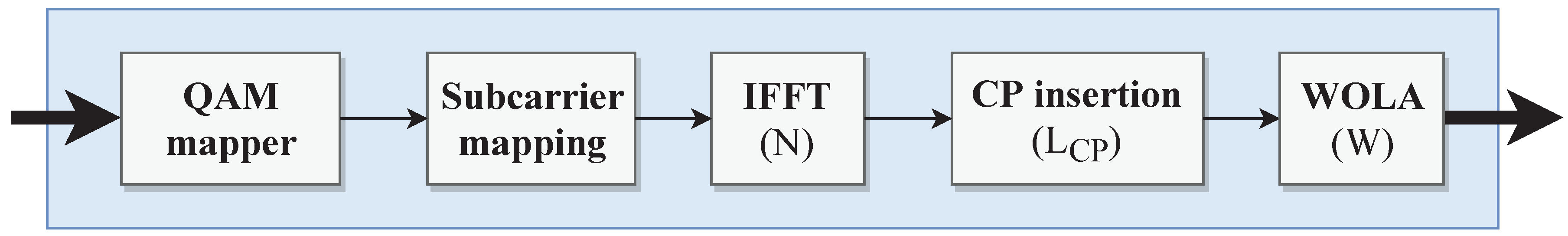
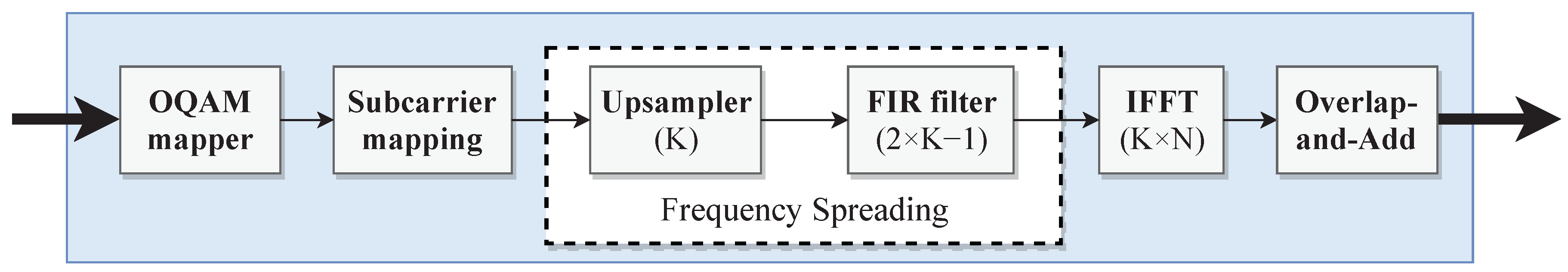
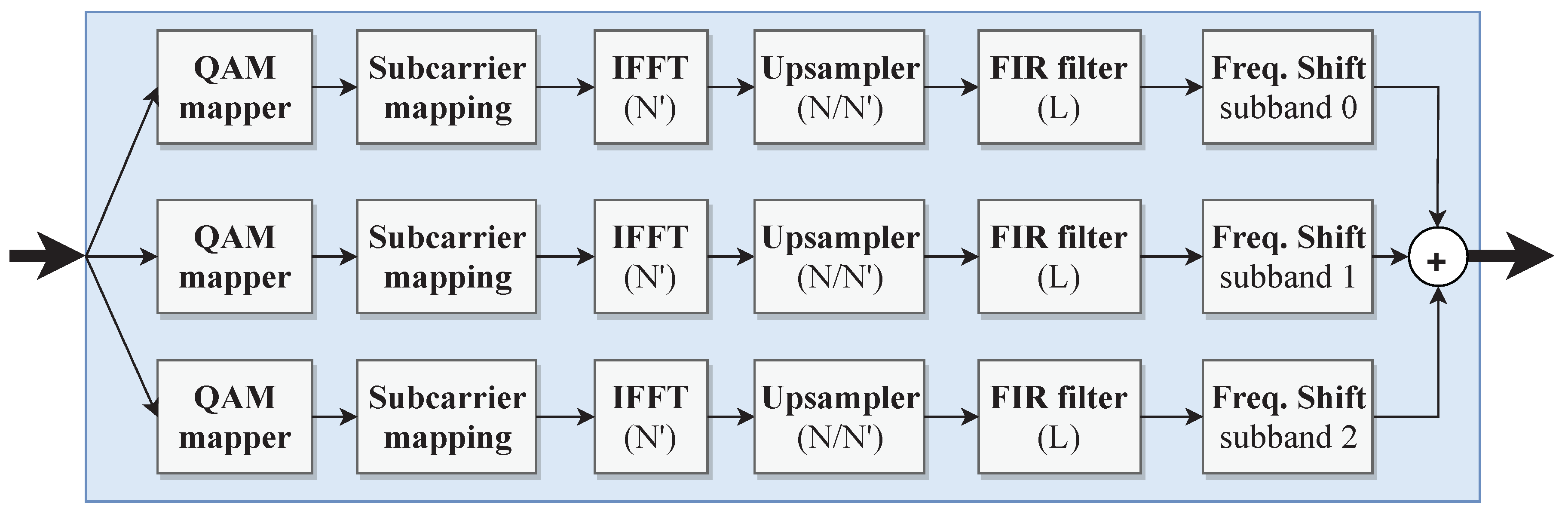
3.1. Baseband Modulation for 5G Waveform Candidates
3.2. Top-Level Architecture
3.3. Limitations and Scope
4. Results and Discussion
5. Conclusions
Author Contributions
Funding
Conflicts of Interest
References
- Lien, S.; Shieh, S.; Huang, Y.; Su, B.; Hsu, Y.; Wei, H. 5G New Radio: Waveform, Frame Structure, Multiple Access, and Initial Access. IEEE Commun. Mag. 2017, 55, 64–71. [Google Scholar] [CrossRef]
- Zaidi, A.A.; Baldemair, R.; Tullberg, H.; Bjorkegren, H.; Sundstrom, L.; Medbo, J.; Kilinc, C.; Silva, I.D. Waveform and Numerology to Support 5G Services and Requirements. IEEE Commun. Mag. 2016, 54, 90–98. [Google Scholar] [CrossRef]
- Jue, G. Exploring 5G Coexistence Scenarios Using a Flexible Hardware/Software Testbed—Application Note. 2017. Available online: https://literature.cdn.keysight.com/litweb/pdf/5992-1917EN.pdf (accessed on 2 October 2018).
- Andrews, J.; Buzzi, S.; Choi, W.; Hanly, S.; Lozano, A.; Soong, A.; Zhang, J. What Will 5G Be? IEEE J. Sel. Areas Commun. 2014, 32, 1065–1082. [Google Scholar] [CrossRef]
- Vipin, K.; Fahmy, S.A. FPGA Dynamic and Partial Reconfiguration: A Survey of Architectures, Methods, and Applications. ACM Comput. Surv. 2018, 51, 72. [Google Scholar] [CrossRef]
- Wirthlin, M.J.; Hutchings, B.L. Improving functional density using run-time circuit reconfiguration. IEEE Trans. Very Large Scale Integr. VLSI Syst. 1998, 6, 247–256. [Google Scholar] [CrossRef]
- Tatsukawa, J. XAPP888—MMCM and PLL Dynamic Reconfiguration; v1.7; Xilinx Inc.: San Jose, CA, USA, 2017. [Google Scholar]
- Bhushan, N.; Ji, T.; Koymen, O.; Smee, J.; Soriaga, J.; Subramanian, S.; Wei, Y. Industry Perspective—5G Air Interface System Design Principles. IEEE Wirel. Commun. 2017, 24, 6–8. [Google Scholar] [CrossRef]
- Yuan, G.; Zhang, X.; Wang, W.; Yang, Y. Carrier aggregation for LTE-advanced mobile communication systems. IEEE Commun. Mag. 2010, 48, 88–93. [Google Scholar] [CrossRef]
- Song, M.; Xin, C.; Zhao, Y.; Cheng, X. Dynamic spectrum access: from cognitive radio to network radio. IEEE Wirel. Commun. 2012, 19, 23–29. [Google Scholar] [CrossRef]
- Kazaz, T.; Van Praet, C.; Kulin, M.; Willemen, P.; Moerman, I. Hardware accelerated SDR platform for adaptive air interfaces. In Proceedings of the ETSI Workshop on Future Radio Technologies: Air Interfaces, Sophia-Antipolis, France, 27–28 January 2016. [Google Scholar]
- Rousseau, B.; Manet, P.; Delavallée, T.; Loiselle, I.; Legat, J.D. Dynamically Reconfigurable Architectures for Software-Defined Radio in Professional Electronic Applications. In Design Technology for Heterogeneous Embedded Systems; Nicolescu, G., O’Connor, I., Piguet, C., Eds.; Springer: Amsterdam, The Netherlands, 2012; pp. 437–455. [Google Scholar]
- Tessier, R.; Pocek, K.; DeHon, A. Reconfigurable Computing Architectures. Proc. IEEE 2015, 103, 332–354. [Google Scholar] [CrossRef]
- Choi, C.; Lee, H. An Reconfigurable FIR Filter Design on a Partial Reconfiguration Platform. In Proceedings of the 2006 First International Conference on Communications and Electronics, Hanoi, Vietnam, 10–11 October 2006; pp. 352–355. [Google Scholar] [CrossRef]
- Delahaye, J.P.; Palicot, J.; Moy, C.; Leray, P. Partial Reconfiguration of FPGAs for Dynamical Reconfiguration of a Software Radio Platform. In Proceedings of the 16th IST Mobile and Wireless Communications Summit, Budapest, Hungary, 1–5 July 2007. [Google Scholar]
- He, K.; Crockett, L.; Stewart, R. Dynamic Reconfiguration Technologies Based on FPGA in Software Defined Radio System. J. Signal Process. Syst. 2011, 69, 75–85. [Google Scholar] [CrossRef]
- Pham, T.H.; Fahmy, S.A.; McLoughlin, I.V. An End-to-End Multi-Standard OFDM Transceiver Architecture Using FPGA Partial Reconfiguration. IEEE Access 2017, 5, 21002–21015. [Google Scholar] [CrossRef]
- Kaltenberger, F.; Knopp, R.; Vitiello, C.; Danneberg, M.; Festag, A. Experimental analysis of 5G candidate waveforms and their coexistence with 4G systems. In Proceedings of the JNCW 2015, Joint NEWCOM/COST Workshop on Wireless Communications, Barcelona, Spain, 14–15 October 2015. [Google Scholar]
- Nadal, J.; Nour, C.A.; Baghdadi, A. Flexible and efficient hardware platform and architectures for waveform design and proof-of-concept in the context of 5G. AEU Int. J. Electron. Commun. 2018, 97, 85–93. [Google Scholar] [CrossRef]
- Chacko, J.; Sahin, C.; Nguyen, D.; Pfeil, D.; Kandasamy, N.; Dandekar, K. FPGA-based latency-insensitive OFDM pipeline for wireless research. In Proceedings of the 2014 IEEE High Performance Extreme Computing Conference (HPEC), Waltham, MA, USA, 9–11 September 2014. [Google Scholar]
- Orozco-Galvan, L.; Parra-Michel, R.; Romero-Aguirre, E. Reconfigurable architecture based on FPGA for OFDM transmitter. In Proceedings of the 2015 7th IEEE Latin-American Conference on Communications, Arequipa, Peru, 4–6 November 2015. [Google Scholar]
- Ferreira, M.L.; Barahimi, A.; Ferreira, J.C. Dynamically reconfigurable LTE-compliant OFDM modulator for downlink transmission. In Proceedings of the 2016 Conference on Design of Circuits and Integrated Systems, Granada, Spain, 23–25 November 2016. [Google Scholar]
- Ferreira, M.L.; Ferreira, J.C.; Huebner, M. A Parallel-Pipelined OFDM Baseband Modulator with Dynamic Frequency Scaling for 5G Systems. In Applied Reconfigurable Computing. Architectures, Tools, and Applications; Voros, N., Huebner, M., Keramidas, G., Goehringer, D., Antonopoulos, C., Diniz, P.C., Eds.; Springer International Publishing: New York, NY, USA, 2018; pp. 511–522. [Google Scholar]
- Nadal, J.; Nour, C.A.; Baghdadi, A. Low-Complexity Pipelined Architecture for FBMC/OQAM Transmitter. IEEE Trans. Circuits Syst. II Express Briefs 2016, 63, 19–23. [Google Scholar] [CrossRef]
- Berg, V.; Doré, J.B.; Noguet, D. A flexible radio transceiver for TVWS based on FBMC. Microprocess. Microsyst. 2014, 38, 743–753. [Google Scholar] [CrossRef]
- Ferreira, M.L.; Ferreira, J.C. Flexible and Dynamically Reconfigurable FPGA-Based FS-FBMC Baseband Modulator. In Proceedings of the 2018 IEEE International Symposium on Circuits and Systems (ISCAS), Florence, Italy, 27–30 May 2018. [Google Scholar]
- Medjkouh, S.; Nadal, J.; Nour, C.A.; Baghdadi, A. Reduced complexity FPGA implementation for UF-OFDM frequency domain transmitter. In Proceedings of the 2017 IEEE International Workshop on Signal Processing Systems (SiPS), Lorient, France, 3–5 October 2017. [Google Scholar]
- Jafri, A.R.; Majid, J.; Zhang, L.; Imran, M.A.; ul islam, M.N. FPGA Implementation of UFMC based baseband transmitter: Case study for LTE 10MHz channelization. Wirel. Commun. Mob. Comput. 2018, 2018, 2139794. [Google Scholar] [CrossRef]
- Knopp, R.; Kaltenberger, F.; Vitiello, C.; Luise, M. Universal filtered multi-carrier for machine type communications in 5G. In Proceedings of the EUCNC 2016, European Conference on Networks and Communications, Athens, Greece, 27–30 June 2016. [Google Scholar]
- Bellanger, M. FS-FBMC: An alternative scheme for filter bank based multi-carrier transmission. In Proceedings of the 2012 5th International Symposium on Communications, Control and Signal Processing, Rome, Italy, 2–4 May 2012. [Google Scholar]
- Vakilian, V.; Wild, T.; Schaich, F.; ten Brink, S.; Frigon, J. Universal-filtered multi-carrier technique for wireless systems beyond LTE. In Proceedings of the 2013 IEEE Globecom Workshops, Toronto, ON, Canada, 24–27 September 2013; pp. 223–228. [Google Scholar] [CrossRef]
- Alves, R.G.; Osorio, P.L.; Swamy, M.N.S. General FFT pruning algorithm. In Proceedings of the 43rd IEEE Midwest Symposium on Circuits and Systems, Lansing, MI, USA, 8–11 August 2000; Volume 3, pp. 1192–1195. [Google Scholar] [CrossRef]
- Xiao, X.; Oruklu, E.; Saniie, J. An Efficient FFT Engine With Reduced Addressing Logic. IEEE Trans. Circuits Syst. II Express Briefs 2008, 55, 1149–1153. [Google Scholar] [CrossRef]
- Silva, N.V.; Oliveira, A.S.R.; Carvalho, N.B. Design and Optimization of Flexible and Coding Efficient All-Digital RF Transmitters. IEEE Trans. Microw. Theory Tech. 2013, 61, 625–632. [Google Scholar] [CrossRef]
- Xilinx Inc. UG909—Vivado Design Suite User Guide: Partial Reconfiguration; Xilinx Inc.: San Jose, CA, USA, 2015. [Google Scholar]
- Claus, C.; Ahmed, R.; Altenried, F.; Stechele, W. Towards Rapid Dynamic Partial Reconfiguration in Video-Based Driver Assistance Systems. In Applied Reconfigurable Computing: Architectures, Tools and Applications; Sirisuk, P., Morgan, F., El-Ghazawi, T., Amano, H., Eds.; Springer: Berlin/Heidelberg, Germany, 2010; pp. 55–67. [Google Scholar]
- Zhang, N.; Brodersen, R.W. The Cost of Flexibility in Systems on a Chip Design for Signal Processing Applications; Technical Report; University of California: Berkeley, CA, USA, 2002. [Google Scholar]
- Akeela, R.; Dezfouli, B. Software-defined Radios: Architecture, state-of-the-art, and challenges. Comput. Commun. 2018, 128, 106–125. [Google Scholar] [CrossRef]
- Moy, C.; Palicot, J. Software radio: A catalyst for wireless innovation. IEEE Commun. Mag. 2015, 53, 24–30. [Google Scholar] [CrossRef]
- FBMC vs. OFDM Modulation—MATLAB & Simulink Example. Available online: https://www.mathworks.com/help/comm/examples/fbmc-vs-ofdm-modulation.html (accessed on 8 August 2018).
- UFMC vs. OFDM Modulation—MATLAB & Simulink Example. Available online: https://www.mathworks.com/help/comm/examples/ufmc-vs-ofdm-modulation.html (accessed on 8 August 2018).
- Schaich, F.; Wild, T.; Chen, Y. Waveform Contenders for 5G—Suitability for Short Packet and Low Latency Transmissions. In Proceedings of the 2014 IEEE 79th Vehicular Technology Conference (VTC Spring), Seoul, Korea, 18–21 May 2014. [Google Scholar]
- ITU-R. Minimum Requirements Related to Technical Performance for IMT-2020 Radio Interface(s); Technical Report M.2410-0; ITU-R: Geneva, Switzerland, 2017. [Google Scholar]


| Mode 1 | Mode 2 | |
|---|---|---|
| # subcarriers, (IFFT size) | 512 | 1024 |
| CP length, | 40 (1st slot symb.) 36 (other symb.) | 80 (1st slot symb.) 72 (other symb.) |
| WOLA samples, | 4 | 6 |
| Mode 1 | Mode 2 | |
|---|---|---|
| # subcarriers, | 512 | 1024 |
| Overlapping factor, | 4 | 4 |
| IFFT size, | 2048 | 4096 |
| Mode 1 | Mode 2 | |
|---|---|---|
| # subcarriers, | 512 | 1024 |
| # subcarriers per PRB | 12 | 12 |
| # active PRBs | 3 | 3 |
| IFFT size, | 64 | 64 |
| Upsampling factor, | 8 | 16 |
| Filter length, | 37 | 73 |
| Filter type | Dolph–Chebyshev (60-dB side lobe attenuation) | |
| Modulator | Mode 1 | Mode 2 | ||||
|---|---|---|---|---|---|---|
| OFDM | FBMC | UFMC | OFDM | FBMC | UFMC | |
| Latency | 2356 | 7743 | 421 | 5172 | 17,469 | 421 |
| Resource | Available (xc7z020) | Static Part | RP | RP | RP | All RPs |
|---|---|---|---|---|---|---|
| Slice | 13,300 | 4210 (31.7%) | 1400 | 2400 | 3200 | 7000 (52.6%) |
| LUT | 53,200 | 10,700 (20.1%) | 5600 | 9600 | 12,800 | 28,000 (52.6%) |
| FF | 106,400 | 13,110 (12.3%) | 11,200 | 19,200 | 25,600 | 56,000 (52.6%) |
| BRAM | 140 | 7.5 (5.4%) | 20 | 40 | 30 | 90 (64.3%) |
| DSP | 220 | 0 | 40 | 80 | 40 | 160 (72.7%) |
| Resource | DFS Overhead | DPR Overhead |
|---|---|---|
| Slice | 24 (0.18%) | 424 (3.19%) |
| LUT | 75 (0.14%) | 938 (1.76%) |
| FF | 79 (0.07%) | 1292 (1.21%) |
| BRAM | 0 | 1.5 (1.07%) |
| DSP | 0 | 0 |
| Resource | Mode 1 | Mode 2 | ||||
|---|---|---|---|---|---|---|
| OFDM | FBMC | UFMC | OFDM | FBMC | UFMC | |
| Slice | 994 | 1575 | 2301 | 1139 | 2210 | 3103 |
| LUT | 2940 | 5103 | 8210 | 3395 | 7876 | 11,780 |
| FF | 2107 | 2307 | 6279 | 2170 | 2284 | 9912 |
| BRAM | 7 | 19 | 11.5 | 10.5 | 40 | 11.5 |
| DSP | 14 | 21 | 18 | 14 | 21 | 18 |
| Nadal et al. [19] | Jafri et al. [28] | |||
|---|---|---|---|---|
| FPGA device | xc7z020 | xc7v2000t | ||
| fclk | Post-Synthesis | Post-Implementation | ||
| 200MHz | 364MHz | |||
| Fixed-point | 16-bit | 16-bit | ||
| precision | ||||
| Waveform | OFDM | FBMC | UFMC | UFMC |
| Numerology | * | * | † | ‡ |
| LUT | 4511 | 8765 | 5945 | 1133 |
| FF | 3006 | 3788 | 3073 | 910 |
| BRAM | n/a | n/a | n/a | 3 |
| DSP | 16 | 32 | 20 | 64 |
| Mode 1 | Mode 2 | |||||
|---|---|---|---|---|---|---|
| OFDM | FBMC | UFMC | OFDM | FBMC | UFMC | |
| 100 | 113 | 148 | 180 | 123 | 161 | 233 |
| 74 | 84 | 119 | 78 | 79 | 155 | |
| 34 | 25 | 60 | 33 | 28 | 77 | |
| 14 | 8 | 30 | 10 | 10 | 39 | |
| RP | RP | RP | |
|---|---|---|---|
| DPR latency | 400 | 677 | 767 |
| Partial bitstream size | 309 | 526 | 596 |
© 2018 by the authors. Licensee MDPI, Basel, Switzerland. This article is an open access article distributed under the terms and conditions of the Creative Commons Attribution (CC BY) license (http://creativecommons.org/licenses/by/4.0/).
Share and Cite
Lopes Ferreira, M.; Canas Ferreira, J. An FPGA-Oriented Baseband Modulator Architecture for 4G/5G Communication Scenarios. Electronics 2019, 8, 2. https://doi.org/10.3390/electronics8010002
Lopes Ferreira M, Canas Ferreira J. An FPGA-Oriented Baseband Modulator Architecture for 4G/5G Communication Scenarios. Electronics. 2019; 8(1):2. https://doi.org/10.3390/electronics8010002
Chicago/Turabian StyleLopes Ferreira, Mário, and João Canas Ferreira. 2019. "An FPGA-Oriented Baseband Modulator Architecture for 4G/5G Communication Scenarios" Electronics 8, no. 1: 2. https://doi.org/10.3390/electronics8010002
APA StyleLopes Ferreira, M., & Canas Ferreira, J. (2019). An FPGA-Oriented Baseband Modulator Architecture for 4G/5G Communication Scenarios. Electronics, 8(1), 2. https://doi.org/10.3390/electronics8010002