Article

A High-Efficiency Low-Power Chip-Based CMOS Liquid Crystal Driver for Tunable Electro-Optic Eyewear

1
Department of Electrical and Computer Engineering, Florida International University, Miami, FL 33174, USA
2
Visual and Biomedical Optics Lab, the Ohio State University, Columbus, OH 43212, USA
3
Versatile Research LLC, Columbus, OH 43220, USA
4
Biomolecular Sciences Institute, Florida International University, Miami, FL 33199, USA
*
Authors to whom correspondence should be addressed.
Electronics 2019, 8(1), 14; https://doi.org/10.3390/electronics8010014
Submission received: 9 November 2018 / Revised: 15 December 2018 / Accepted: 17 December 2018 / Published: 22 December 2018
(This article belongs to the Section Microelectronics)

Abstract

:
A high-efficiency low-power chip-based liquid crystal (LC) driver has been successfully designed and implemented for adaptive electro-optic eyewear including tunable vision correction devices (eyeglass, contact lens, intraocular lens, occluder, and prism), phoropter, iris, head-mounted display, and 3D imaging. The driver can generate a 1 kHz bipolar square wave with magnitude tunable from 0 V to 15 V to change the lens focus adaptively. The LC driver output magnitude is controlled by a reference DC voltage that is manually tunable between 0 and 3 V. A multi-mode 1×/2×/3×/4×/5× charge pump is developed for DC-DC conversion to expand the output range with a fast-sink function implemented to regulate the charge pump output. In addition, a new four-phase H-bridge driving scheme is employed to improve the DC/AC inverter efficiency. The LC driver has been successfully implemented and tested as an IC chip (8.6 mm × 8.6 mm) using AMS 0.18 μm High-Voltage CMOS technology.

1. Introduction

Electrically tunable liquid crystal (LC) lenses, prisms, irises, and occluders are very useful in vision-related applications, such as eyeglass [1], contact lens [2], phoropter [3,4], treatment for amblyopia and strabismus [5], head-mounted display [6,7,8,9,10] (virtual reality, augmented reality, and mixed reality), and 3D imaging [1,11]. The electrically tunable power of the LC lenses and prisms (or the transmission of the occluders) can be adjusted with varying refractive indices (or the scattering) due to re-orientations of LC directors controlled by the applied electric fields. For eyewear applications, relatively small and safe drive voltages but still a large enough range (e.g., up to 15 Vrms), compactness and low power consumption are critical for effective LC lens applications [1,12,13,14,15]. According to the literature, it has been demonstrated that LC lenses based on patterned electrodes for phase modulation provide the best optical wavefront and imaging quality with smaller aberrations. In this case, different voltages are applied to the electrodes to form the desired phase profile. This indicates that multiple output channels are needed for the LC driver. LC lenses usually require a standard square wave with adjustable RMS voltage amplitudes as a controller for adaptive varifocal tuning. Typically, a small size battery, and a DC-AC converter with adjustable output amplitude can be used to generate a desired driving voltage for effective LC varifocal length control. The switched-capacitor charge pump (SC-CP) regulators [16], which can either step up or step down the input voltage, are the preferable form of the DC-DC converter for generating square waves of various amplitudes, since they can be easily implemented with integrated circuits. However, traditional charge pumps, which have a fixed multiplication ratio, are not flexible in generating a wide range of different output voltages for LC lens applications. In this work, a multi-mode charge pump will be used to improve the LC driver efficiency in voltage generation. By alternating the gate control voltages of the switching transistors, the charge pump can connect flying capacitors in parallel or series during charging and discharging periods, and consequently multiple conversion ratios can be obtained. The optimum mode of the charge pump is automatically determined by the input voltage. Once the optimum mode is selected, a bang-bang control topology can be further used to regulate the output voltage of the charge pump. However, a charge pump outputs DC signals only. We need to convert them to square waveforms (AC) for applications in electro-optic lens.
To convert a DC voltage to a square wave, one can use an inverter to periodically switch the polarity of a DC input generated by the charge pump. Two simplest topologies of the inverters are half-bridge and full-bridge inverters. Implementing a full-bridge inverter requires two more transistors than a half-bridge inverter, but the peak-to-peak output voltage is twice as large as that of the half-bridge inverter.
In this work, a new chip-based LC lens driver has been designed for low power portable applications. The system is powered by a single lithium-ion button cell with a voltage of 3 V, while the output RMS voltage of the square wave is adjustable from 0 V to 15 V through the control of the input reference voltage. The input reference voltage can be changed by turning a knob of a trimpot manually. The amplitude of the LC driver output voltage is supposed to be 5 times as large as the reference voltage. The charge pump automatically changes the conversion mode and regulates the output voltage to generate the required DC voltage level; the DC voltage is then converted to AC voltage by the full-bridge inverter. The high output RMS voltage (up to 15 V) is crucial for LC driver in tunable-focus lens control. The high-voltage CMOS (HV-CMOS) process for chip fabrication is gaining popularity recently for many high-voltage applications [17]. An important feature of the HV-CMOS process is the existence of a deep n-well (DNW) in a moderately p-doped bulk allowing the circuits to be isolated from high voltages. The LC driver in this work will be implemented with AMS HV CMOS technology to achieve the high voltage output for lens focus control.
The rest of this paper is organized as follows. The system architecture and the detailed design of the CMOS LC driver are introduced in Section 2. The methodology for improving the design and some of the system simulation results are presented in Section 3. The LC driver chip implementation and testing results are given in Section 4. Finally, some conclusions are drawn in Section 5.

2. LC Device Driver Design

The system architecture of the proposed chip-based LC driver is shown in Figure 1a. The system consists of a trimpot, a mode selector, a gate controller, a level shifter, a charge pump regulator, a comparator, a voltage divider, a fast sinker, and an inverter.
The reference voltage (VREF) can be adjusted between 0 V to 3 V by tuning the trimpot manually. This voltage is used for the operating mode selection at the mode selector and is also used to adjust the charge pump output voltage according to the mode selection rule specified in Table 1.
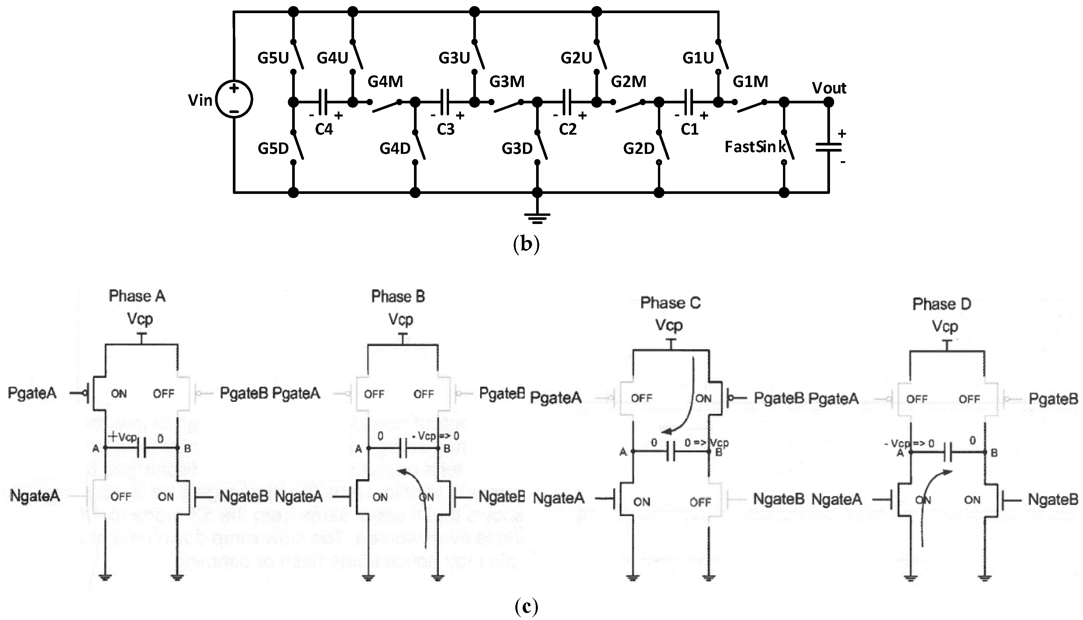
For a specific value of VREF, one of the mode selection signals is automatically enabled according to the selection rule in Table 1, and all other mode signals are disabled. The structure of the proposed multi-mode charge pump is shown in Figure 1b. The operation mode is determined by the gate voltages applied to the transistors at the charge pump through Gate Control module in Figure 1a. It should be noted that the charge pump output voltage VDC in Figure 1a is determined by the voltage divider and the feedback regulator [18,19]. With the voltage divider ratio chosen as 1/5, the output voltages VDC and VAC (RMS) are 5 times as large as the input voltage VREF regardless of the charge pump operation mode [20]. The multi-mode charge pump in Figure 1a simply provides a wide range of output voltages.
The charge pump operates in two phases, i.e., charging and discharging phases, for each of the five multiplication modes. In the charging phase, all the flying capacitors are parallel-connected and charged to the voltage of Vin, while in the discharging phase, the flying capacitors are series-connected to the input source and release charges to the output and the ground. The transistor switching states in Figure 1b according to the modes and the phases are presented in Table 2, where “X” indicates the corresponding transistor is turned on.
The Level Shift module in Figure 1a is used to shift the voltage levels of transistor gate control voltages to ensure each transistor operates in an appropriate region. The divider and the comparator in Figure 1a are the feedback components to regulate the output voltage of the charge pump (VDC) to generate the desired output voltage amplitude by the charge pump. If the divider voltage ratio is set to 1: N, the charge pump output voltage will be amplified N-1 times larger than the input voltage [21]. An internal oscillator is designed with a typical current-starved ring VCO to generate 10 kHz and 1 kHz clock signals. 10 kHz clock is used to pace the charge pump output so that the output responds to the input voltage change promptly. The 1 kHz clock controls the pass transistors in the H-bridge inverter to ensure that 1 kHz bipolar square wave will be generated for driving LC devices.
Other innovative function modules in the LC driver design such as the closed-loop output regulator, H-bridge inverter and fast charge-sinker will be detailed in the next section.

3. Design Features and Simulation Results

Several innovative features have been included in the LC driver design to improve its performances in power consumption, response time and efficiency. Specifically, the design advantages using the closed-loop output regulator, H-bridge inverter, fast charge sinker and others are to be deliberated.

3.1. Bang-Bang Closed-Loop Output Regulator

Linear regulation is widely used to control charge pump output in a closed loop. However, a linear regulator could be very inefficient and lead to a possible large drop in the output voltage [22,23,24,25]. In this design, we use the bang-bang control topology to regulate the charge pump’s output. Since the regulator is a purely capacitive switch, theoretically it could achieve near 100% power efficiency. The range of the voltage bang is determined by the hysteresis voltage of the comparator. By carefully designing this voltage regulator, we can achieve a bang within the output voltage ripple requirement. Moreover, by using the bang-bang control method, we can use a rail-to-rail comparator instead of the traditional rail-to-rail OPAMP in the control loop for much reduced power consumption. The rail-to-rail comparator consumes much less power since it does not need a feedback loop that is always stable. The power optimization of this rail-to-rail comparator should be balanced with the requirement that its slew rate is high enough to respond in time to the worst-case output voltage drop of the charge pump.

3.2. Low-Power H-Bridge Inverter

A new low-power H-bridge driving scheme is used to minimize the power consumption of the H-bridge inverter. The operation period of the H-bridge is composed of four phases, which are shown in Figure 1c. In phases B and D, both PMOS switches are turned off and both NMOS switches are turned on. For the negative voltage output, the charges are drawn from the ground only without consuming energy of the power supply. In phases A and C, the supply voltage only needs to charge the capacitor from 0 to +VCP, instead of charging from −VCP to +VCP, where VCP is the desired charge pump output voltage. The gate control waveform A of the H-bridge in Figure 1c is the 1 kHz square waveform generated by the internal oscillator and the control waveform B is the inverted version of waveform A. Compared with the regular two-phase H-bridge inverter [26,27,28,29], the power consumption of the new H-bridge inverter is much reduced.

3.3. Fast Charge Sinker

When the charge pump needs to lower its output voltage, it generally discharges through the output load. As the load current may be very low, discharging could be time-consuming and lead to a slow response to input change [30,31]. To alleviate this issue, we introduce a charge-sinking transistor in the charge pump to facilitate the discharging process. Without the fast sinking circuit, the simulation result shows that it takes 82 ms for the driver to switch from the 5× mode to 4× mode. For lower output voltages, the response times are even longer. The extended ramp-down times for the charge pump may not be acceptable in lens applications since flashing or dimming may become noticeable by the person who wears the lenses. Therefore, in this work a fast sinking circuit is implemented to address this issue. The fast sink logic detects the step-down edge of the reference signal and then generates a one-shoot pulse to turn on the sinking transistor in the charge pump. The one-shoot circuit is a RC-delay network capable of generating a sink triggering pulse with a certain width. The sizing of the delay RC circuit is determined by the time constant of the sinking transistor resistance and the equivalent output capacitance. With the new design, the simulation shows that the output sinking process can be accomplished within 62 µs.

3.4. System Opitmization and Simulations

Besides the innovative modules described above used in the design, the LC driver in Figure 1a has been optimized intensively in terms of minimizing power consumption and operation efficiency. The length and width of each transistor are carefully selected and optimized to improve the power consumption and efficiency [32,33,34]. The multiple types of level-shifting circuits are designed to minimize the consumed power and to maximize the circuit efficiency.
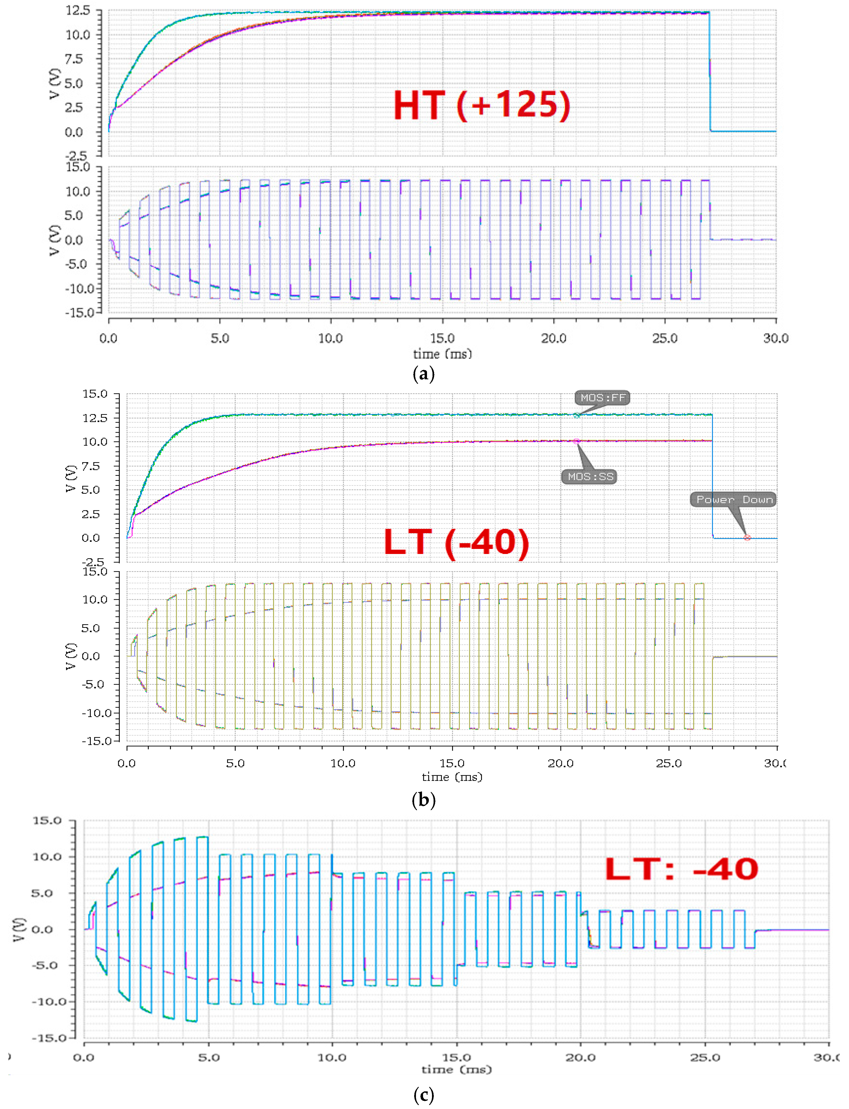
The regulated multi-modes LC driver with improved efficiency is designed with AMS 0.18 μm 20 V VGS, 50 V VDS High-Voltage CMOS technology and simulated with Cadence. Figure 2a–b shows the simulation results of the LC driver output with the input voltage VREF switching from 0 V to 2.5 V at high (125 °C) and low temperatures (−40 °C), respectively. The top curves in the figures are the output of the charge pump simulated at FF corner (blue line) and SS corner (purple line). The bottom curves are the H-Bridge inverter outputs at FF and SS corners. With the input voltage at 2.5 V, the output voltage amplitudes of both the charge pump and H-bridge are about 12.5 V, which is about 5 times as large as the input voltage, as expected. In addition, the frequency of the square wave at the output of the H-Bridge inverter is exactly 1 kHz. For the FF MOS model, the charge pump ramp-up time is about 3.2 ms; for the worst-case SS MOS model, the charge pump ramp-up times are much longer, especially at low temperature. The results for the TT MOS model are much closer to those of the FF model. When the input voltage switches from 2.5 V to 0 V, with the fast sinking circuit enacted, the charge pump ramp-down time is about 60 µs, which is almost unnoticeable from the shown waveforms.
Figure 2c is the driver output voltages in response to staircase input control voltages changing in the order of 0 V, 2.5 V, 2 V, 1.5 V, 1.0 V. 0.5 V and 0 V sequentially with a duration of 5 ms at each input voltage level. The output voltage amplitudes (in RMS) are about 5 times as large as the input voltages with a frequency of 1 kHz. When the input voltage increases from 0 V to 2.5 V, the output ramp-up time is observed to be 3.2 ms. When the input voltage drops and the fast-sink feature is enabled, the driver output responds almost instantly.

4. Implementation and Testing Results

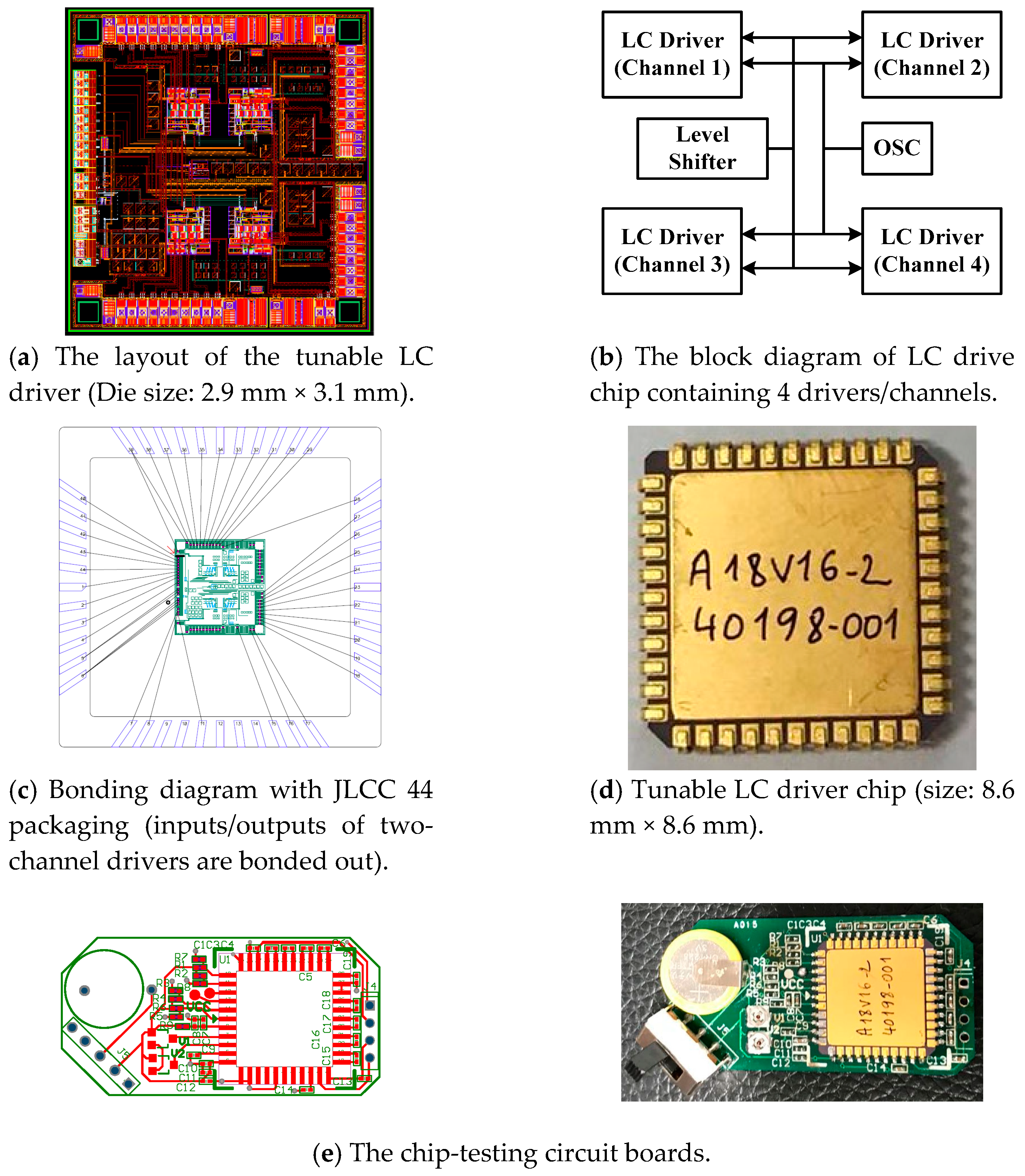
The designed LC driver has been fabricated into a chip with AMS 0.18 µm high-voltage CMOS (H18A6) process with the maximum gate and drain voltages up to 20 V and 50 V, respectively. The fabrication was completed in the form of MPW contracted through CMP Corp. The whole design was floor-planned, laid out and verified with Cadence IC 6.1.6 [35] and AMS design kit Hitkit 4.11 [36].
The layout of the driver chip is shown in Figure 3a. The whole chip consists of four independent LC drivers (or channels) with each of them controlled by a separate reference voltage for lens tuning. The circuit diagram of the whole chip is shown in Figure 3b. The 4 LC drivers shown in the figure are the same as discussed in the previous sections. The level shifting circuit and the oscillators generating 10 kHz and 1 kHz clocks are shared by 4 LC drivers in the chip. To limit the chip size and the number of input/output pins for portable applications, we had only the input/outputs of two channels bonded for packaging. Two LC driving channels currently are sufficient for some lens applications such as eyeglass control with each of the channels tuning one of two glass lenses [1,37]. Figure 3c shows the 44-pin bonding diagram for chip packaging, and Figure 3d is the actual chip fabricated by the AMS.
The testing circuit board has been developed for the chip fabricated with H18 CMOS process and is shown in Figure 3e. Besides the chip, the circuit board [38] also includes a 3 V lithium-ion battery, 8 external 10 µF flying capacitors used for two charge pumps, two input reference voltage generators that can be adjusted between 0 and 3 V manually, and other auxiliary components. The output waveforms of the testing circuit board are applied to a 10 µF capacitor to simulate LC driving load as well as the actual LC cells and lenses. Some of the testing parameters and results are listed in Table 3. The ramp-up and ramp-down times of the charge pumps are basically observed to be the same as the simulation results. The ramp-down time of the charge pump is very small due to enaction of the fast sinking circuit. The power consumption of the LC driver (each channel) was recorded to be about 1.6 mw; and the total power consumed by the entire chip is about 3.5 mw, slightly more than 2 times as much as each channel power. The low power consumption of the designed chip allows the circuit to operate for months or even years without replacing the battery [39].
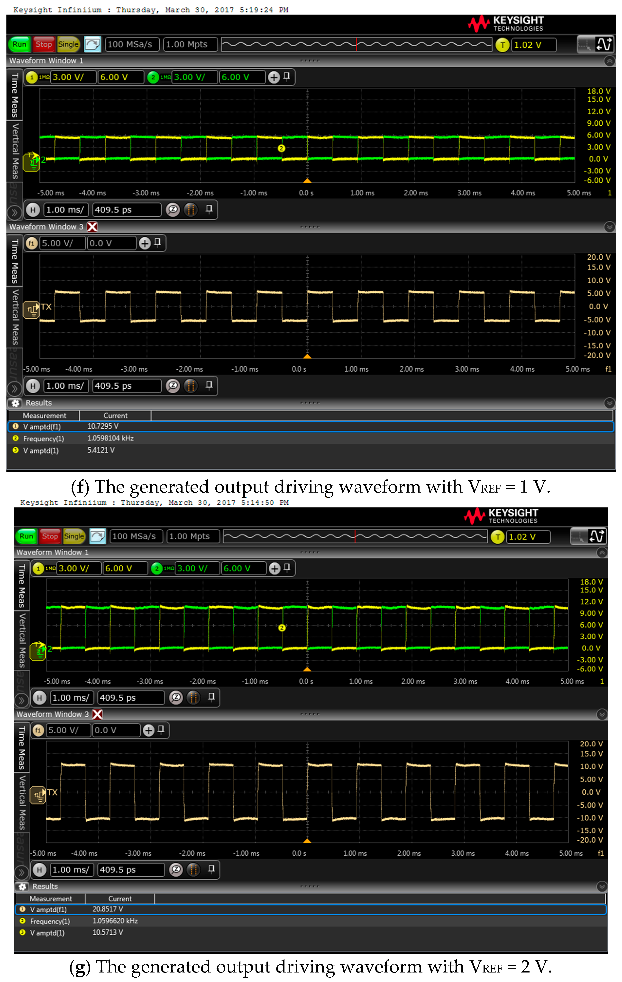
The output driving waveforms from one of the channel testing results with two different input control voltages are displayed in Figure 3f,g. The waveforms indicate that the output voltage in RMS is amplified to be 5 times as large as the input voltage. The output square wave’s frequency is about 1 kHz.
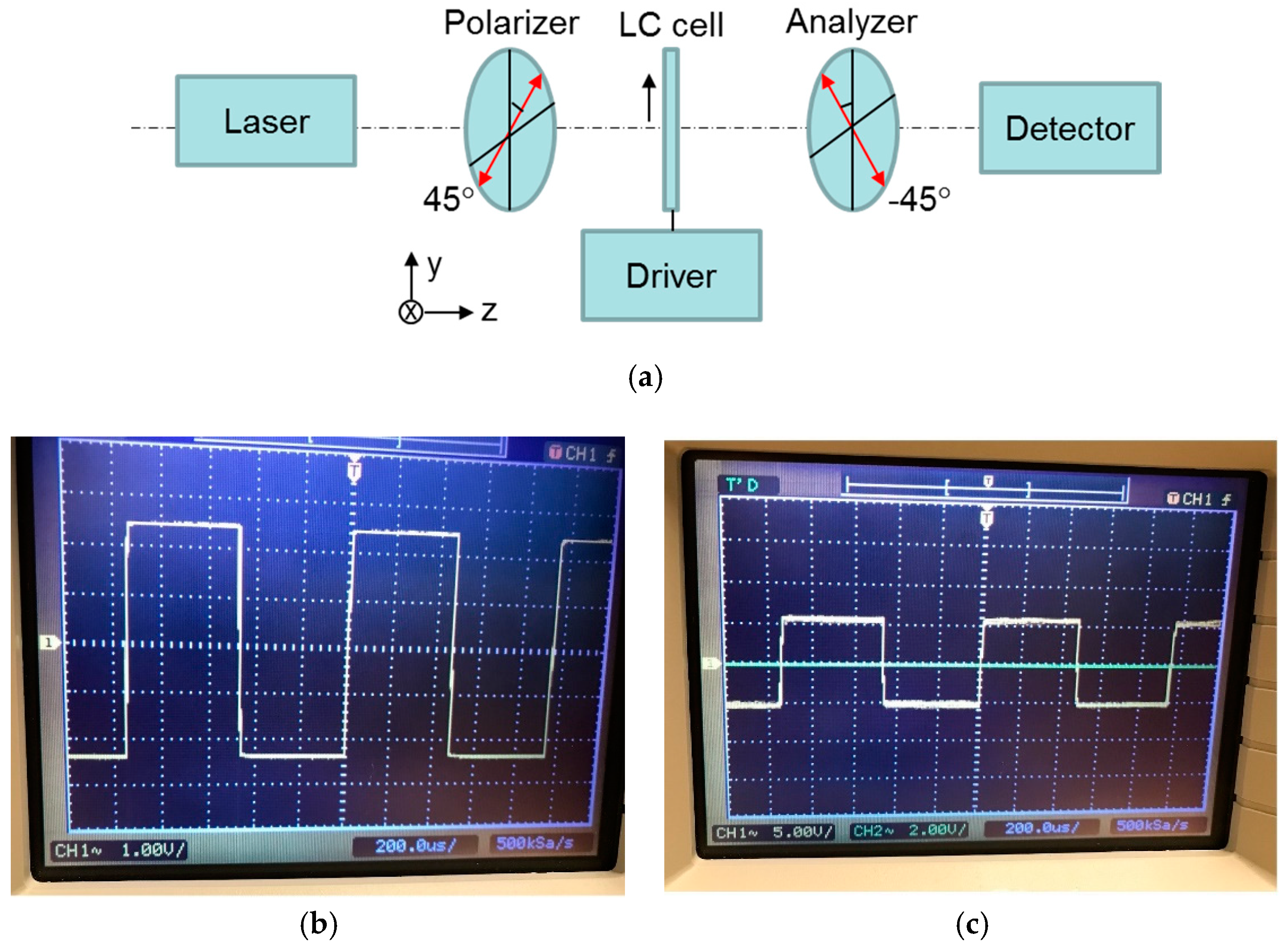
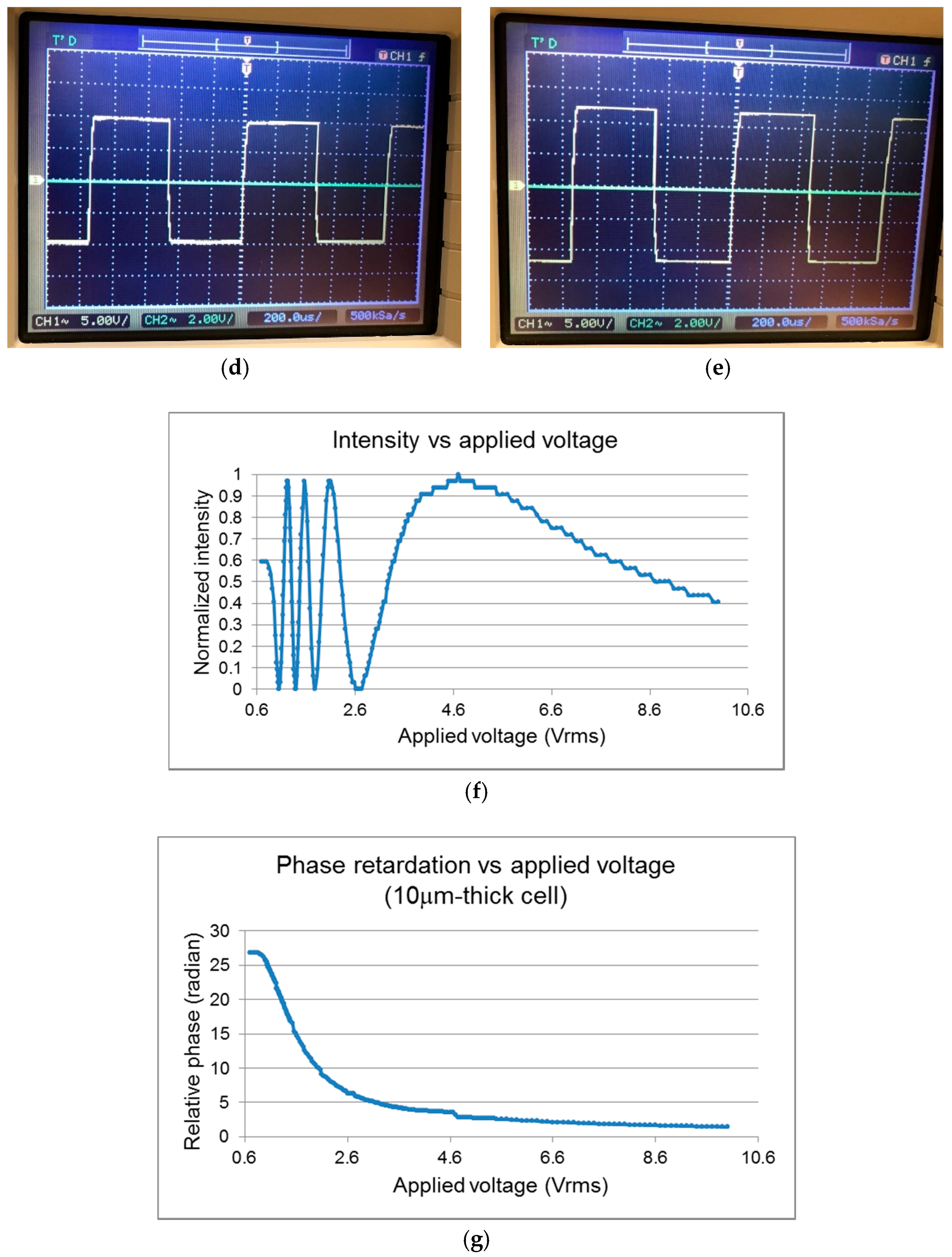
To test if the designed LC driver operates properly for actual lens focus control, the output of the circuit board in Figure 3e was applied to a 10 µm-thick nematic LC cell in a standard crossed polarizer setup shown in Figure 4a. The LC material is sandwiched between two glass substrates uniformly coated with a thin transparent and conductive layer of indium tin oxide (ITO), and the output voltage from the driver is applied to the two ITO layers. A collimated He-Ne laser working at 543.5 nm is used as the lighting source. The LC device is placed between two crossed polarizers, which are aligned with their transmission axes at 45° and −45° respectively to the vertical (y) axis. A detector connected to a computer is employed to record the intensity values. Initially, the long axis of the liquid crystal is close to the vertical direction. With the applied voltage above the threshold value, the liquid crystal molecules will start to tilt, generating different birefringence between the ordinary and extraordinary components of the light. For each position, the irradiance at the detector changes with the change of the phase difference ( Φ ) between the ordinary and extraordinary components at the exit surface of the device. The intensity value I is given by
I = I 0 sin 2 ( Φ / 2 )
where I0 is the incident intensity. When no voltage is applied to the electrodes, a certain amount of light will be transmitted through the analyzer. Specifically, when a voltage is applied so that Φ = π , the transmission reaches the maximum, and when Φ = 2 π , the transmission reaches the minimum. Figure 4b–e shows 4 examples of the square wave displayed on the oscilloscope.
Figure 4f shows the variation of the normalized intensity under the impact of 1 kHz LC driver voltages (RMS) changing from 0.5 V to 10 V that are generated by the IC-designed driver in Figure 3e. It demonstrates that the desired electro-optic responses of the LC device are obtained when appropriate driving voltages are applied. The result also indicates the LC driver works as expected for the LC cell foci control. Figure 4g illustrates the relative phase retardation as a function of the applied voltage, which is obtained based on the data in Figure 4f and the above mentioned intensity—phase relationship.

5. Conclusions

A chip-based low-power liquid crystal device driver for portable adaptive eyewear applications has been successfully designed and tested in this work. The challenging demand for high-voltage output for chip-based driver has been met in this design. These distinct features make the use of this device possible in a wide range of wearable LC devices and applications. To improve the performance of the device, we use a few innovative circuit components in the design. A multi-modes charge pump has been designed to generate a desired range of voltage output. Bang-bang control topology has been used for the effective regulation of the output voltage from the charge pump. An innovative charge-sinking circuit is designed to greatly facilitate charge-pump ramp-down time. A new H-bridge inverter has been used for improving DC-to-AC conversion efficiency. The advantage of the new chip-based driver is that it is capable of generating the largest driving voltage amplitude range (30 V in peak-to-peak swing) in the literature for more robust adaptive lens control. On the other hand, the larger output voltage swing would slightly increase the power consumption of the drive chip. With successful design and implementation of this new chip-based LC driver, we envision that various kinds of adaptive eyewear have been made possible. The eyewear can be for vision correction and treatment, or image display, or retinal imaging. In the future design, the dimensions of the packaged chip and the circuit board will be further shrunk to make them installable in the frame of regular eyeglasses to achieve fully-adaptive closed-loop smart eyewear.

Author Contributions

Project conceptualization & funding acquisition, G.L.; project administration & supervision, G.L.; methodology & investigation, H.D. and G.L.; writing/original draft preparation, H.D. and G.L.; writing-review and editing, G.L and H.D.

Funding

This research was supported in part by the NIH National Eye Institute through grant R01EY020641 (G.L.), the State of Ohio TVSF fund through grant TECG20160460 (G.L.), and Versatile Research LLC.

Conflicts of Interest

The authors declare no conflict of interest.

References

  1. Li, G. Adaptive lens. Prog. Opt. 2010, 55, 199–283. [Google Scholar]
  2. Bailey, J.; Morgan, P.B.; Gleeson, H.F.; Jones, J.C. Switchable liquid crystal contact lenses for the correction of presbyopia. Crystals 2018, 8, 29. [Google Scholar] [CrossRef]
  3. Li, G.; Han, Z.; Lan, G. Adaptive Electro-optic lenses for vision correction and assessment, and eye imaging. Investig. Ophthalmol. Vis. Sci. 2012, 53, 3584. [Google Scholar]
  4. Riza, N.A.; Admin, M.J.; Riza, M.N. Eye vision testing system and eyewear using micromachines. Micromachines 2015, 6, 1690–1709. [Google Scholar] [CrossRef]
  5. Li, G. Adaptive electro-optic occluder with variable transmission and contrast. Investig. Ophthalmol. Vis. Sci. 2018, 59, 4124. [Google Scholar]
  6. Kramida, G. Resolving the vergence-accommodation conflict in head-mounted displays. IEEE Trans. Vis. Comput. Graph. 2016, 22, 1912–1931. [Google Scholar] [CrossRef]
  7. Suyama, S.; Date, M.; Takada, H. Three-dimensional display system with dual-frequency liquid-crystal varifocal lens. Jpn. J. Appl. Phys. 2000, 39, 480–484. [Google Scholar] [CrossRef]
  8. Wang, Y.J.; Chen, P.-J.; Liang, X.; Lin, Y. Augmented reality with image registration, vision correction and sunlight readability via liquid crystal devices. Sci. Rep. 2017, 7, 433. [Google Scholar] [CrossRef]
  9. Love, G.D.; Hoffman, D.M.; Hands, P.J.W.; Gao, J.; Kirby, A.K.; Banks, M.S. High-speed switchable lens enables the development of a volumetric stereoscopic display. Opt. Express 2009, 17, 15716–15725. [Google Scholar] [CrossRef]
  10. Yamaguchi, M. Full-parallax holographic light-field 3-D displays and ınteractive 3-D touch. Proc. IEEE 2017, 105, 947–959. [Google Scholar] [CrossRef]
  11. Lan, G.; Li, G. Design of high-performance adaptive objective lens with large optical depth scanning range for ultrabroad near infrared microscopic imaging. Biomed. Opt. Express 2015, 6, 3362–3377. [Google Scholar] [CrossRef] [PubMed] [Green Version]
  12. Li, G.; Penmatsa, V. Large-aperture harmonic diffractive adaptive liquid crystal lens for vision care. In Proceedings of the Bio-Optics: Design and Application (BODA) 2015, Vancouver, BC, Canada, 12–15 April 2015. [Google Scholar]
  13. Li, G.; Mathine, D.L.; Valley, P.; Äyräs, P.; Haddock, J.; Giridhar, M.S.; Schwiegerling, J.; Meredith, G.; Kippelen, B.; Honkanen, S.; et al. Switchable electro-optic diffractive lens with high efficiency for ophthalmic applications. Proc. Natl. Acad. Sci. USA 2006, 103, 6100–6104. [Google Scholar] [CrossRef] [PubMed] [Green Version]
  14. Li, G.; Valley, P.; Ayras, P.; Mathine, D.L.; Honkanen, S.; Peyghambarian, N. High-efficiency switchable flat diffractive ophthalmic lens with three-layer electrode pattern and two-layer via structures. Appl. Phys. Lett. 2007, 90, 111005. [Google Scholar] [CrossRef]
  15. Li, G.; Valley, P.; Giridhar, M.S.; Mathine, D.; Meredith, G.; Haddock, J.; Kippelen, B.; Peyghambarian, N. Large-aperture switchable thin diffractive lens with interleaved electrode pattern. Appl. Phys. Lett. 2006, 89, 141120. [Google Scholar] [CrossRef]
  16. Pan, F.; Samaddar, T. Charge Pump Circuit Design, 1st ed.; McGraw-Hill Education: New York, NY, USA, 2006. [Google Scholar]
  17. Feigl, S. Latest results on the HV-CMOS pixel sensor in the AMS H18 process. In Proceedings of the 2015 IEEE Sensors Conference, Busan, Korea, 1–4 November 2015. [Google Scholar]
  18. Musunuri, S.; Chapman, P.L.; Zou, J.; Liu, C. Design issues for monolithic DC-DC converters. IEEE Trans. Power Electron. 2005, 20, 639–649. [Google Scholar] [CrossRef]
  19. Eberle, W.; Zhang, Z.; Liu, Y.; Sen, P. A practical switching loss model for buck voltage regulators. IEEE Trans. Power Electron. 2009, 24, 700–713. [Google Scholar] [CrossRef]
  20. Aloisi, W.; Palumbo, G. Efficiency model of boost DC-DC PWM converters. Int. J. Circuit Theory Appl. 2005, 33, 419–432. [Google Scholar] [CrossRef]
  21. Hasan, A.; Gregori, S. Modeling of step-up DC-DC converters to formulate design guidelines for optimization. In Proceedings of the IEEE Canadian Conference on Electrical and Computer Engineering (CCECE), Quebec, QC, Canada, 3–6 May 2009; pp. 911–915. [Google Scholar]
  22. Greco, N.; Spina, N.; Fiore, V.; Ragonese, E.; Palmisano, G. A galvanically isolated DC-DC converter based on current-reuse hybrid-coupled oscillators. IEEE Trans. Circuits Syst. II 2017, 64, 56–60. [Google Scholar] [CrossRef]
  23. Liou, W.; Lin, S.C.; Lin, C.Y.; Sun, C.H. Monolithic low-EMI CMOS DC-DC boost converter for portable applications. IEEE Trans. VLSI Syst. 2014, 22, 420–424. [Google Scholar] [CrossRef]
  24. Mitrovic, N.; Enne, R.; Zimmermann, H. An integrated current sensing circuit with comparator function for a buck DC-DC converter in HV-CMOS. In Proceedings of the 2016 IEEE International Conference on Electronics, Circuits and Systems (ICECS), Monte Carlo, Monaco, 11–14 December 2016. [Google Scholar]
  25. Tanzawa, T.; Tanaka, T. A dynamic analysis of the Dickson charge pump circuit. IEEE J. Solid-State Circuits 1997, 20, 1231–1240. [Google Scholar] [CrossRef]
  26. Wens, M.; Cornelissens, K.; Steyaert, M. A fully-integrated 0.18 mm CMOS DC-DC step-up converter, using a bondwire spiral inductor. In Proceedings of the IEEE European Solid-State Circuits Conference (ESSCIRC), Munich, Germany, 11–13 September 2007; pp. 268–271. [Google Scholar]
  27. Kossov, O. Comparative analysis of chopper voltage regulators with LC filter. IEEE Trans. Magn. 1968, 4, 712–715. [Google Scholar] [CrossRef]
  28. Du, S.; Liu, J.; Lin, J.; He, Y. A novel DC voltage control method for STATCOM based on hybrid multilevel H-bridge converter. IEEE Trans. Power Electron. 2013, 28, 101–111. [Google Scholar] [CrossRef]
  29. Sepahvand, H.; Liao, J.; Ferdowsi, M.; Corzine, K.A. Capacitor voltage regulation in single-DC-source cascaded H-bridge multilevel converters using phase-shift modulation. IEEE Trans. Ind. Electron. 2013, 60, 3619–3626. [Google Scholar] [CrossRef]
  30. Shaltout, A.; Gregori, S. Design trade-offs of integrated polygonal inductors for DC-DC power converters. In Proceedings of the IEEE International Symposium on Circuits and Systems (ISCAS), Baltimore, MD, USA, 28–31 May 2017; pp. 1–4. [Google Scholar]
  31. Cuk, S. A new zero-ripple switching DC-to-DC converter and integrated magnetics. IEEE Trans. Magn. 1983, 19, 57–75. [Google Scholar] [CrossRef] [Green Version]
  32. Grebene, A. Bipolar and MOS Analog Integrated Circuit Design; Wiley: Hoboken, NJ, USA, 2003. [Google Scholar]
  33. Baker, R.J. CMOS Circuit Design, Layout, and Simulation; Wiley IEEE Press: Hoboken, NJ, USA, 2010. [Google Scholar]
  34. Reinhard, D. Introduction to Integrated Circuit Engineering; Houghton Mifflin Co.: Boston, MA, USA, 1987. [Google Scholar]
  35. Cadence Design Systems. Available online: https://www.cadence.com/ (accessed on 8 November 2018).
  36. Annual Report—CMP: Circuits Multi-Projets. 2016. Available online: https://mycmp.fr/IMG/pdf/cmp_annualreport_2016.pdf (accessed on 8 November 2018).
  37. Li, G. Adaptive Lens for Vision Correction. U.S. Patent 8,587,734 B2, 8 March 2010. International Patent WO 102295A1, 8 March 2010. [Google Scholar]
  38. Khan, M.; Islam, M.; Deng, H. Design of a Re-configurable RFID Sensing Tag as a Generic Sensing Platform (GSP) Towards the Future Internet of Things (IoT). IEEE Internet Things J. 2014, 1, 300–310. [Google Scholar] [CrossRef]
  39. Khan, M.; Deng, H. Design and Prototyping a Smart Deep Brain Stimulator: An Autonomous Neuro-Sensing and Stimulating Electrode System. IEEE Intell. Syst. 2017, 32, 14–27. [Google Scholar] [CrossRef]
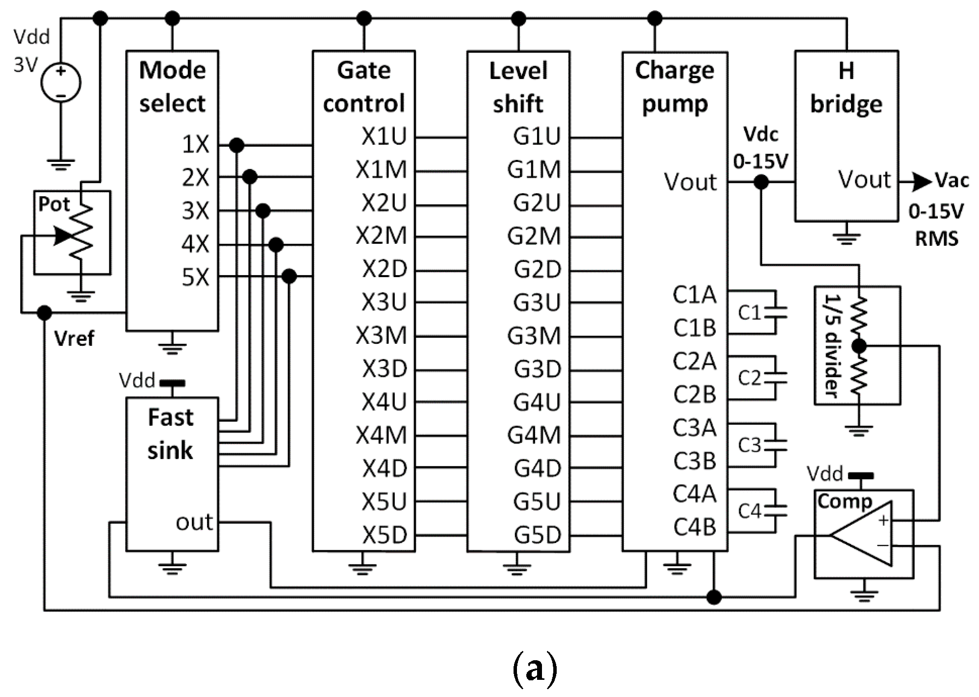
Figure 1. (a) System architecture of the LC driver; (b) Structure of the proposed multi-mode charge pump; (c) Switching scheme with a new low-power H-Bridge inverter.
Electronics 08 00014 g001aElectronics 08 00014 g001b
Figure 2. (a) The simulation results of the LC driver output (bottom curves) and the charge pump outputs (The top curve in blue in the FF corner and the top one in purple in the SS corner) at high temperature (125 °C); (b) The simulation results of the LC driver output (bottom curves) and the charge pump outputs (The top curve in blue in the FF corner and the top one in purple in the SS corner) at low temperature (−40 °C); (c) The driver output voltage generated in response to staircase control voltage (above) at low temperature (−40 °C).
Electronics 08 00014 g002
Figure 3. (ad) LC Driver Chip Design Results; (e) the circuit boards for testing LC driver chip (The left: the chip testing circuit PCB viewed from top. The right: the circuit board testing the designed LC driver chip); (fg) Chip testing results: the driving waveforms out of the H-bridge for various input reference voltages VREF (The top curves: two differential outputs of half H-bridges; the bottom curve: the full H-bridge output).
Electronics 08 00014 g003aElectronics 08 00014 g003b
Figure 4. (a) Setup for testing the electro-optic response of the liquid crystal cell; (be), Some of the 1 kHz waveforms (in oscilloscope screenshot) generated by the LC driver used for driving the LC cell in (a) with (b)VRMS = 2.5 V; (c) VRMS = 5 V; (d) VRMS = 10 V; and (e) VRMS = 12.5 V; (f) Intensity modulation as a function of the applied voltage; (g) Relative phase retardation generated by the liquid crystal cell as a function of the applied voltage.
Electronics 08 00014 g004aElectronics 08 00014 g004b
Table 1. LC driver mode selection: the reference voltage vs. output voltage.
VREF (DC)Selected ModeVAC (RMS)
0.0 V < VREF ≤ 0.6 V0 V < VAC ≤ 3 V
0.6 V < VREF ≤ 1.2 V3 V < VAC ≤ 6 V
1.2 V < VREF ≤ 1.8 V6 V < VAC ≤ 9 V
1.8 V < VREF ≤ 2.4 V9 V < VAC ≤ 12 V
2.4 V < VREF ≤ 3.0 V 12 V < VAC ≤ 15 V
Table 2. Charge pump transistor switching states control according to the modes and phases.
TransistorCharging PhaseDischarging Phase
Mode
G1UXXXXXX----
G1MX----XXXXX
G2U--XXX-X---
G2M------XXXX
G2D-XXXX-----
G3U---XX--X--
G3M-------XXX
G3D--XXX-----
G4U----X---X-
G4M--------XX
G4D---XX-----
G5U---------X
G5D----X-----
Table 3. Some testing parameters and results of the designed 2-channel LC driver chip.
ParameterMinTypicalMaxUnit
Input voltage source2.73.03.3V
charge pump (CP) output0-15.0V
Working temperature−4023125°C
Output frequency-1 k-Hz
CP rump-up time-3.2-ms
CP rump-down time-62.0-µs
Total power consumption-3.5-mW
Power consumption per channel-1.6-mW