Article

A Hybrid Current Mode Controller with Fast Response Characteristics for Super Capacitor Applications

Department of Control and Instrumentation Engineering, Korea University of Transportation, Chungju 27469, Korea
*
Author to whom correspondence should be addressed.
Electronics 2019, 8(1), 112; https://doi.org/10.3390/electronics8010112
Submission received: 18 December 2018 / Revised: 13 January 2019 / Accepted: 15 January 2019 / Published: 19 January 2019
(This article belongs to the Special Issue Advanced Power Conversion Technologies)

Abstract

:
A wide-bandwidth current-controller is required for the fast charging and discharging of applications containing super capacitors. To accomplish this, peak current mode is generally used due to the speed of its response characteristics. On the other hand, peak current mode control must be provided with a slope compensation function to restrain sub-harmonic oscillations. However, if the controlled output voltage is varied, the slope must be changed accordingly. Nonetheless, it is not easy to change the slope for every change in output voltage. Another solution involves the slope being set at the maximum value, which results in a slow response. Therefore, in this paper, a hybrid mode controller was proposed that uses a peak current and a newly-specified valley current. Using the proposed hybrid mode control, sub-harmonic oscillation did not occur for duty cycles larger than 0.5 and response times were fast.

1. Introduction

Recently, research and development in the field of renewable energy application is becoming increasingly active due to the increase in environmental pollution and the exhaustion of fossil fuels. In response to social trends, there is a growing interest in environmentally-friendly electric vehicles and hybrid vehicles for the rail or the automotive industries. In particular, various research projects have been carried out to investigate regenerative braking, which stores wasted energy by converting kinetic energy into electric energy when the vehicle decelerates [1,2,3,4]. As research into regenerative braking becomes more active, the importance of fast storage of electric energy is increasing. Due to long charging and discharging cycles and a long lifetime, super capacitors are being increasingly used instead of batteries in many applications [5,6,7]. For energy storage system applications that use super capacitors, a voltage controller with quick response characteristics is required for fast charging of the super capacitor. It is desirable to use a combination of a peak current mode controller, an inner loop current controller, and an outer loop voltage controller to achieve fast response characteristics. However, use of the peak current mode control method causes a sub-harmonic oscillation problem to occur when the duty is 0.5 or more [8,9,10,11,12].
To prevent this sub-harmonic oscillation, the slope compensation method has been proposed along with the use of a triangular wave [13,14,15,16]. It should be noted that since the range of the slope compensation depends on the input and output voltages, the compensation slope should be changed according to these input or output voltage conditions. However, since the charging voltage of a super capacitor changes suddenly, it is not easy to change the compensation slope with the actual output voltage.
Therefore, it is common to maintain the maximum compensation slope to prevent sub-harmonic oscillation for all input and output voltage conditions. However, this leads to another problem, since as the compensation slope becomes larger, the response time of the current controller decreases [17,18]. Another method has been proposed to solve this sub-harmonic oscillation problem: the current control method using peak and valley currents [19]. Figure 1 shows the proposed current control method [19] using maximum and minimum currents. This method makes use of two upper and lower triangular waves. This method compares the peak current to the upper triangular wave and the valley current to the lower triangular wave to control current. Since the slope of the upper and lower waveforms is influenced by the input and output voltages, the compensation slope changes from time to time in hardware depending on the input and output voltage conditions. In this paper, a novel hybrid current mode controller is proposed that does not make use of slope compensation and which possesses fast response characteristics. The proposed controller makes use of the minimum current determined to maintain the maximum current and constant PWM (Pulse-Width-Modulation) frequency instead of using the slope compensation method. In Section 2, the slope compensation values are analyzed in terms of eliminating sub-harmonic oscillations and the problems associated with using the slope compensation method are discussed. In Section 3, a hybrid current mode control scheme is proposed. In Section 4 and Section 5, the proposed hybrid controller is analyzed and evaluated using Powersim (PSIM) simulations and experimental evaluation.

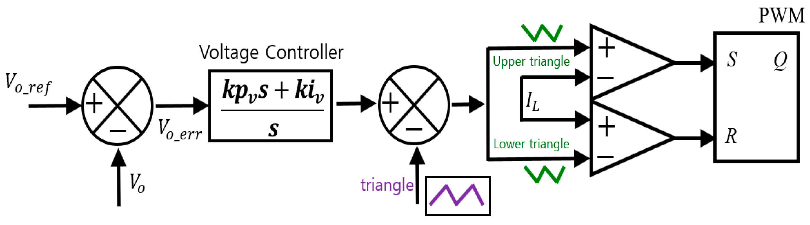
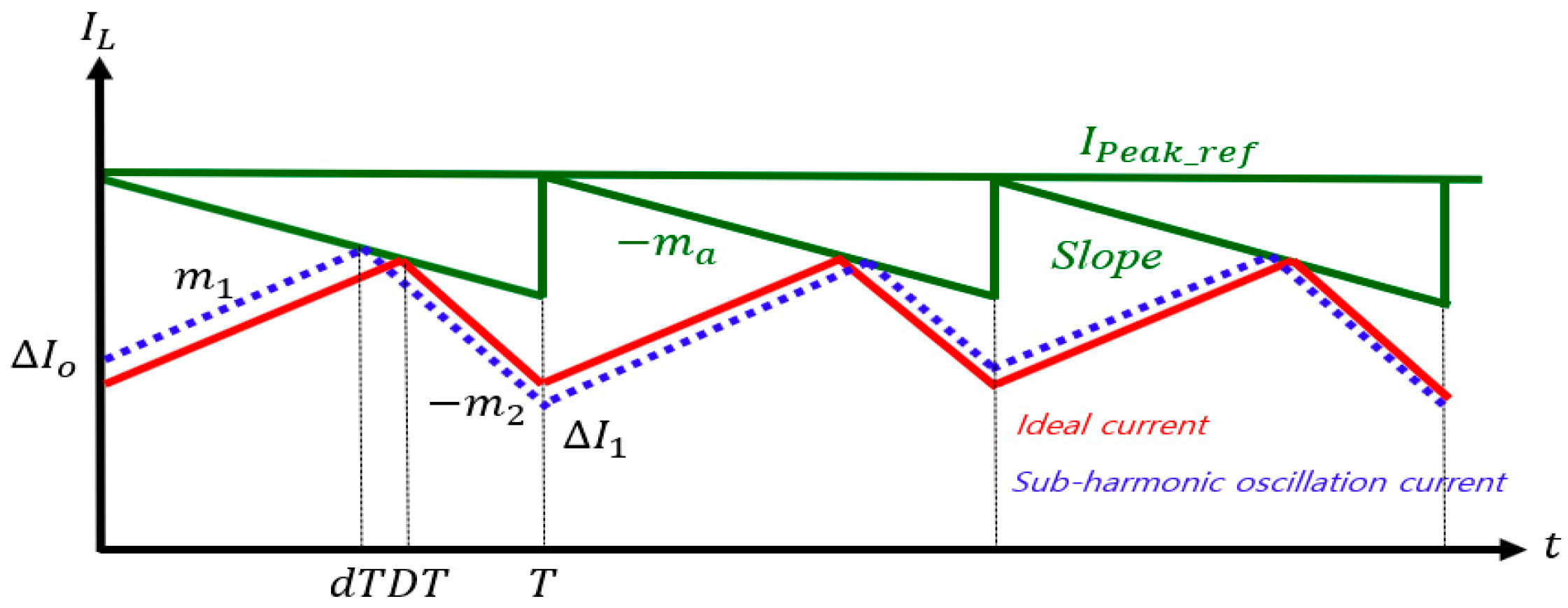
2. Slope Compensating Method for the Elimination of Sub-Harmonic Oscillation

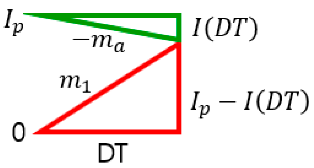
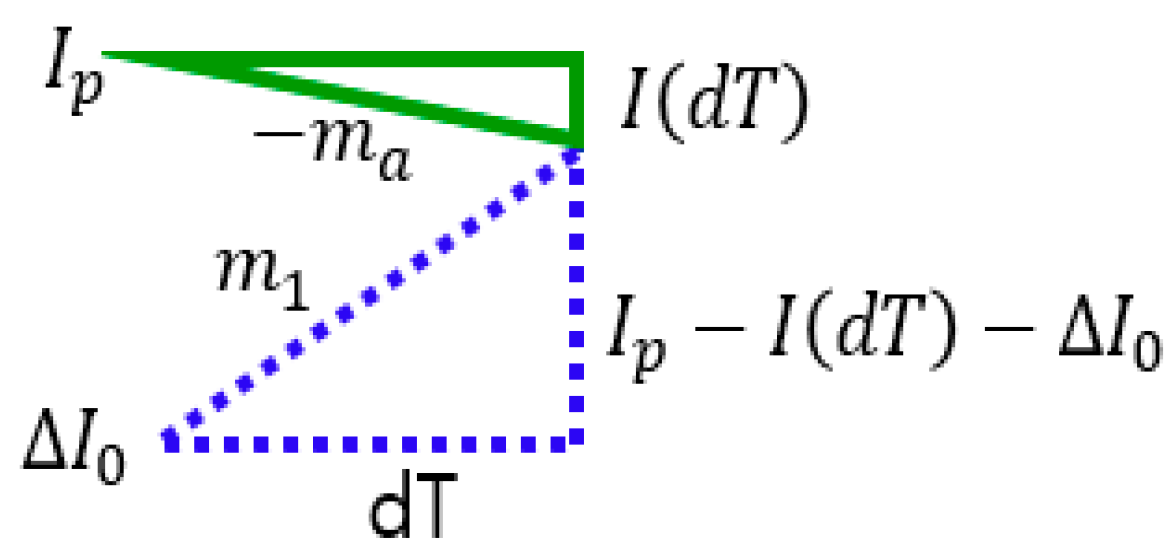
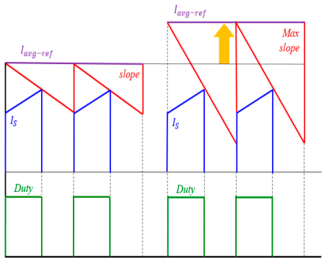
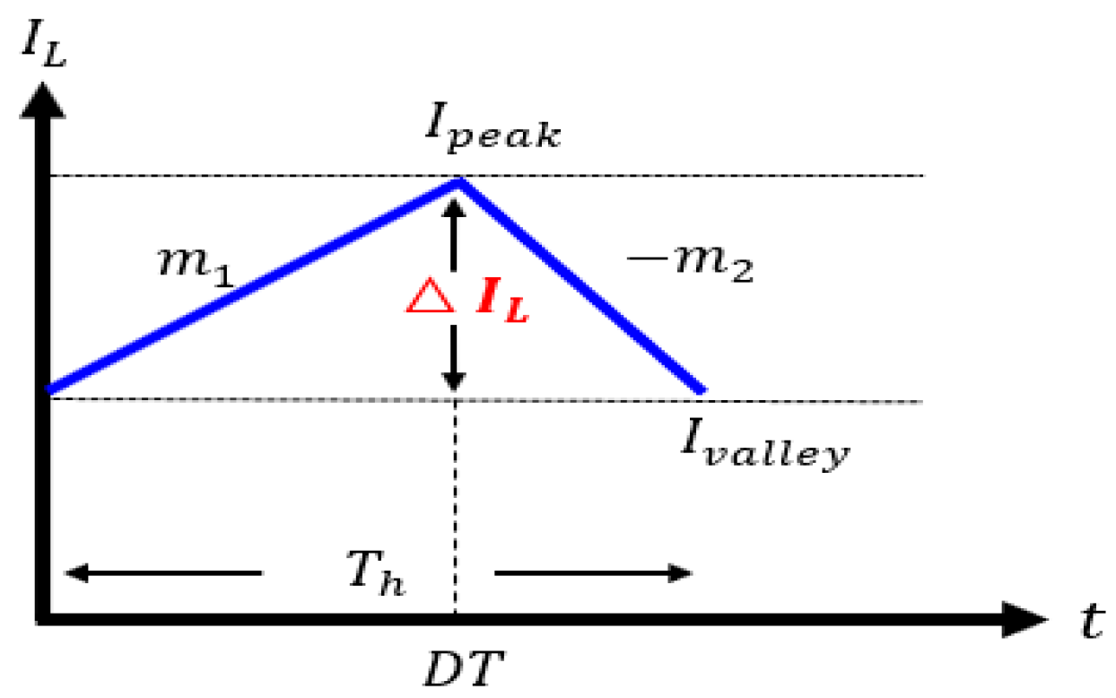
2.1. Slope Value Selection Method for Slope Compensation

Figure 2 shows the operating principle of a typical peak current mode controller. In Figure 2, the PWM output signal Q is generated via an RS (Reset Set) flip-flop. The clock pulse input to the set terminal of the RS flip-flop turns the transistor on through the output signal Q every fixed period. The transistor is turned off by the reset signal when the input current and the maximum current command signal become equal. The converter current increases when the transistor is on and decreases when the transistor is off. When the duty cycle is small, the converter current increases during the on state; the current decreases sufficiently during the off state. On the contrary, when the duty cycle is large, the clock pulse—which is a set signal—turns the transistor on at regular intervals and the current does not decrease sufficiently. If the current cannot be completely reduced at every cycle, the perturbation magnitude of the converter current becomes large, resulting in sub-harmonic oscillation. Figure 3 shows the slope compensation method used to solve the sub-harmonic oscillation problem. The slope compensation method is a method of subtracting the triangular wave from the maximum current command and comparing it with the input current. Using this method, the current perturbation magnitude of the present PWM period becomes smaller than the previous PWM period, thereby eliminating the sub-harmonic oscillation. To eliminate the sub-harmonic oscillation, the current fluctuation coefficient due to the current perturbation should be less than 1.
In Figure 3, m 1 is the slope at which the current rises, m 2 is the slope at which the current falls, m a is the slope of the triangular wave, I p is the maximum current command, I n is the magnitude of the current perturbation at the nth period, DT is the rise time of the ideal current, and dT represents the rise time of the sub-harmonic oscillation perturbation current.
Figure 4 shows a triangular waveform comparing the ideal current and the slope compensation in the rising current period shown in Figure 3. Equation (1) represents the sum of m1 obtained from the ideal current and ma obtained from the slope. Figure 5 shows a triangular waveform comparing the slope compensation and the current generated by the sub-harmonic oscillation in the rising current period shown in Figure 3. Equation (2) represents the sum of m1 obtained from the sub-harmonic oscillation current and ma obtained from the slope:
m 1 + m a = I p D T
m 1 + m a = I p I o d T
Therefore, if the Equations (1) and (2) are summarized, the relationship between m 1 and m a in the rising current period is expressed by Equation (3):
m 1 + m a = I o T ( D d )
Figure 6 shows a triangular waveform comparing the ideal current and slope compensation in the falling current period shown in Figure 3. Equation (4) represents the value obtained by subtracting m2 obtained from the ideal current and ma obtained from the slope. Figure 7 shows a triangular waveform comparing the slope compensation and the current generated by the sub-harmonic oscillation in the falling current period shown in Figure 3. Equation (5) represents the value obtained by subtracting m2 obtained from the sub-harmonic oscillation current and ma obtained from the slope.
m a m 2 = I p + I ( T ) D T
m a m 2 = I p + I ( T ) I 1 d T
Therefore, if Equations (4) and (5) are summarized, the relationship between m 2 and m a in the falling current period is expressed by Equation (6):
m a m 2 = I 1 T ( D d )
Equation (7) summarizes Equation (3)—which is the relationship between slope m 1 and slope m a —and Equation6—which is the relationship between slope m 2 and slope m a . If the slope compensation value satisfies Equation (7), the magnitude of the current perturbation becomes smaller than 1, and thus, the sub-harmonic oscillation phenomenon is eliminated.
I 1 = m a + m 2 m 1 + m a I 0 m a + m 2 m 1 + m a 1 m a m 2 m 1 2

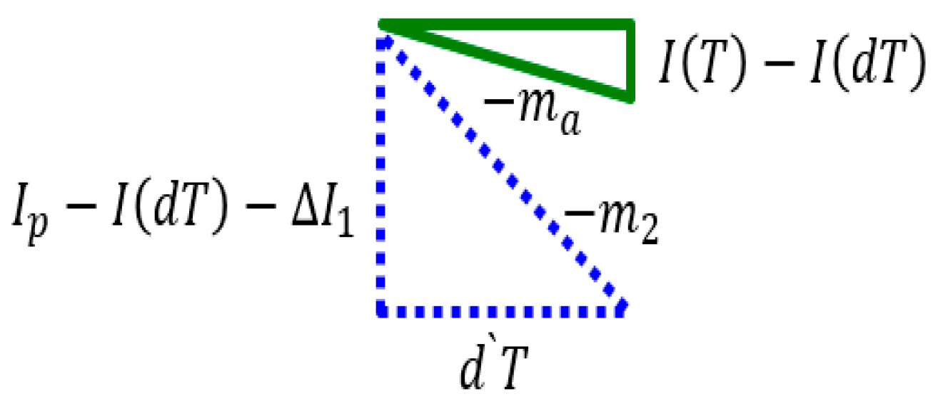
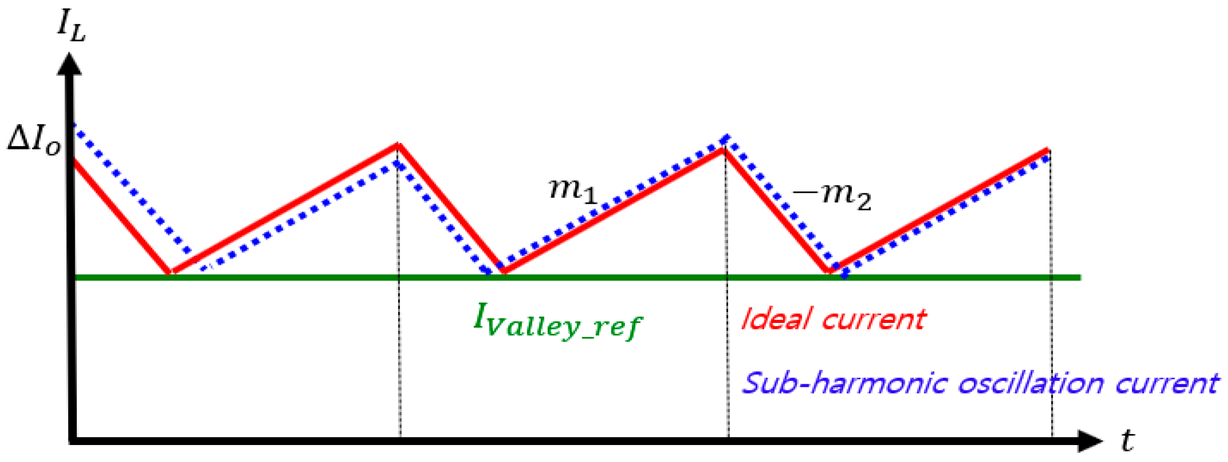
2.2. Problems with the Slope Compensation Method

Equation (8) shows the rising and falling slope of the inductor current in the boost converter; where m 1 is the slope of the rising inductor current, m 2 is the slope of the falling inductor current, V g is the input voltage, V o is the output voltage, and L is the value of the boost converter inductor.
Substituting Equation (8) into Equation (7) leads to Equation (9). It can be seen that when the output voltage is changed in Equation (9), the slope must also change at the same time. However, it is not always easy to change the slope in accordance with the actual output voltage value in systems that experience sudden voltage changes, such as in super capacitor systems. Figure 8 and Figure 9 show the inductor current waveforms when the input and output voltages are changed using a fixed slope compensation method:
m 1 = V g L , m 2 = V o V g L
m a > V o V g 2 L
Section A of the graph in Figure 8 shows the inductor current waveform before the input/output voltage is changed and Section B shows the inductor current waveform after the input/output voltage is changed. Fixed slope compensation for constant input and output voltage conditions is obtained by applying Equation (9). If the input and output voltages are changed, the slope is out of range and compensation cannot be properly performed. In order to solve this problem, the slope compensation is generally set to the maximum value at which no sub-harmonic oscillation occurs. Figure 10 shows the effect on the output duty cycle when normal and maximum slope compensations are used. Since the maximum slope is higher than the normal slope, it meets the slope compensation value first and forms a small duty cycle, thus, the average current command from the voltage controller must be high to achieve the same duty cycle. Here, the current value is compensated much more than for the original value, and the current controller experiences a response delay.

3. Designing a Controller with a Fast Response Time

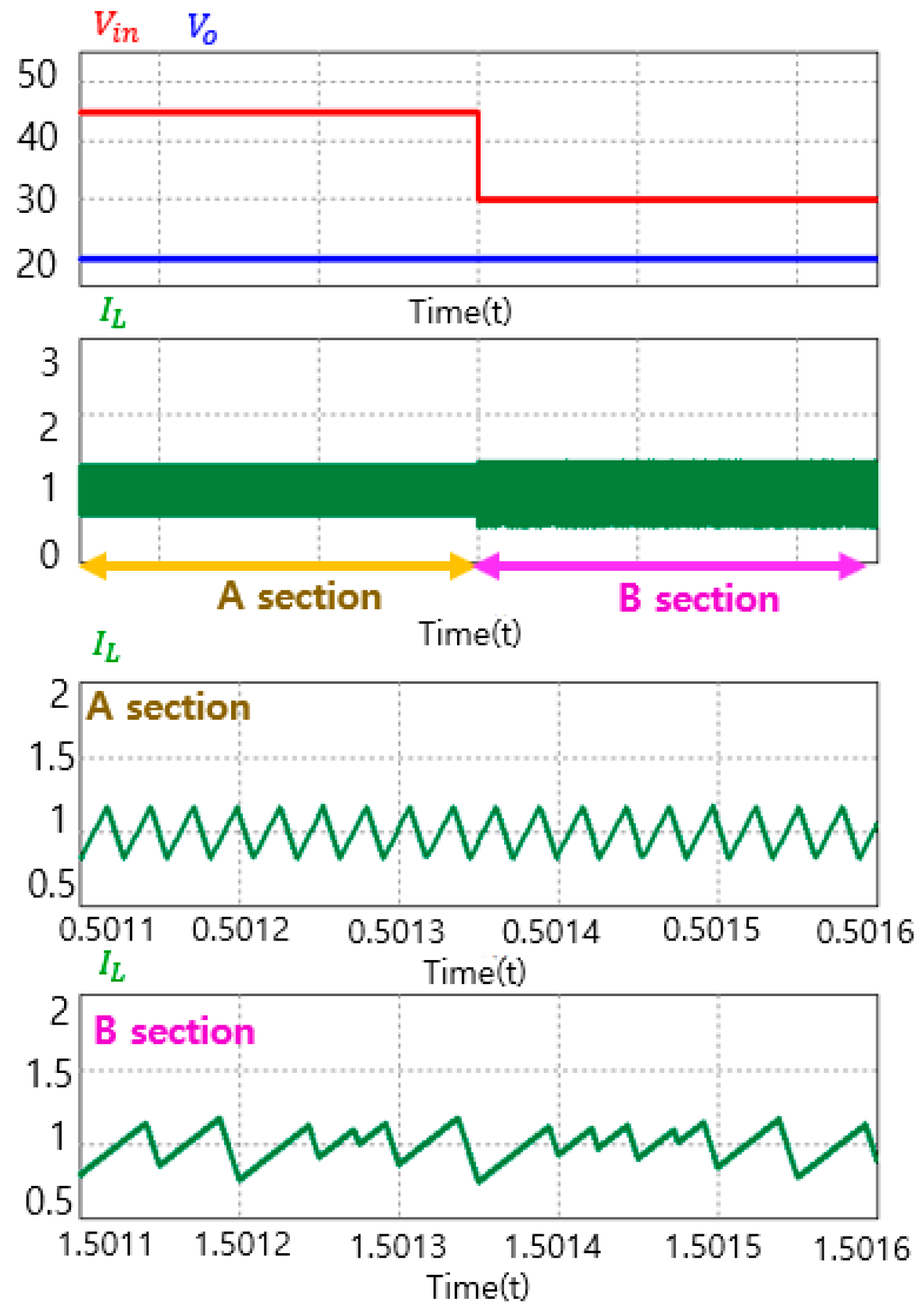
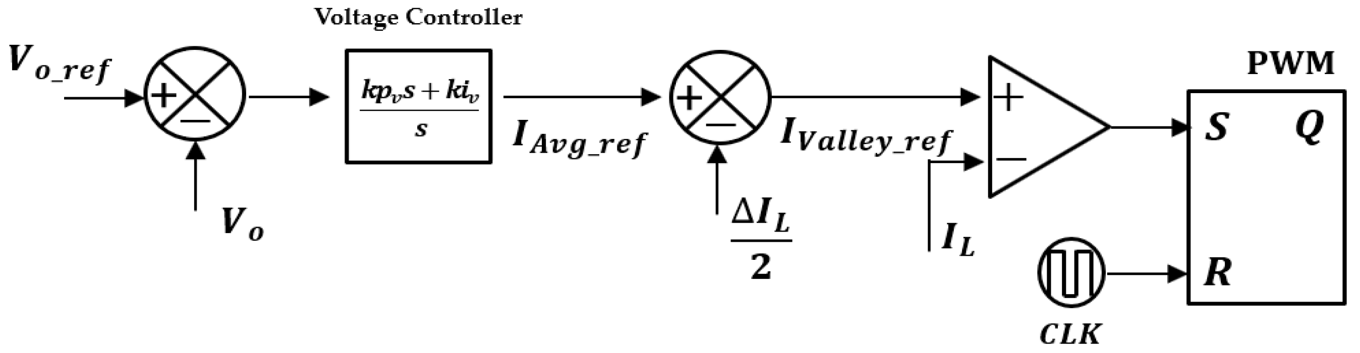
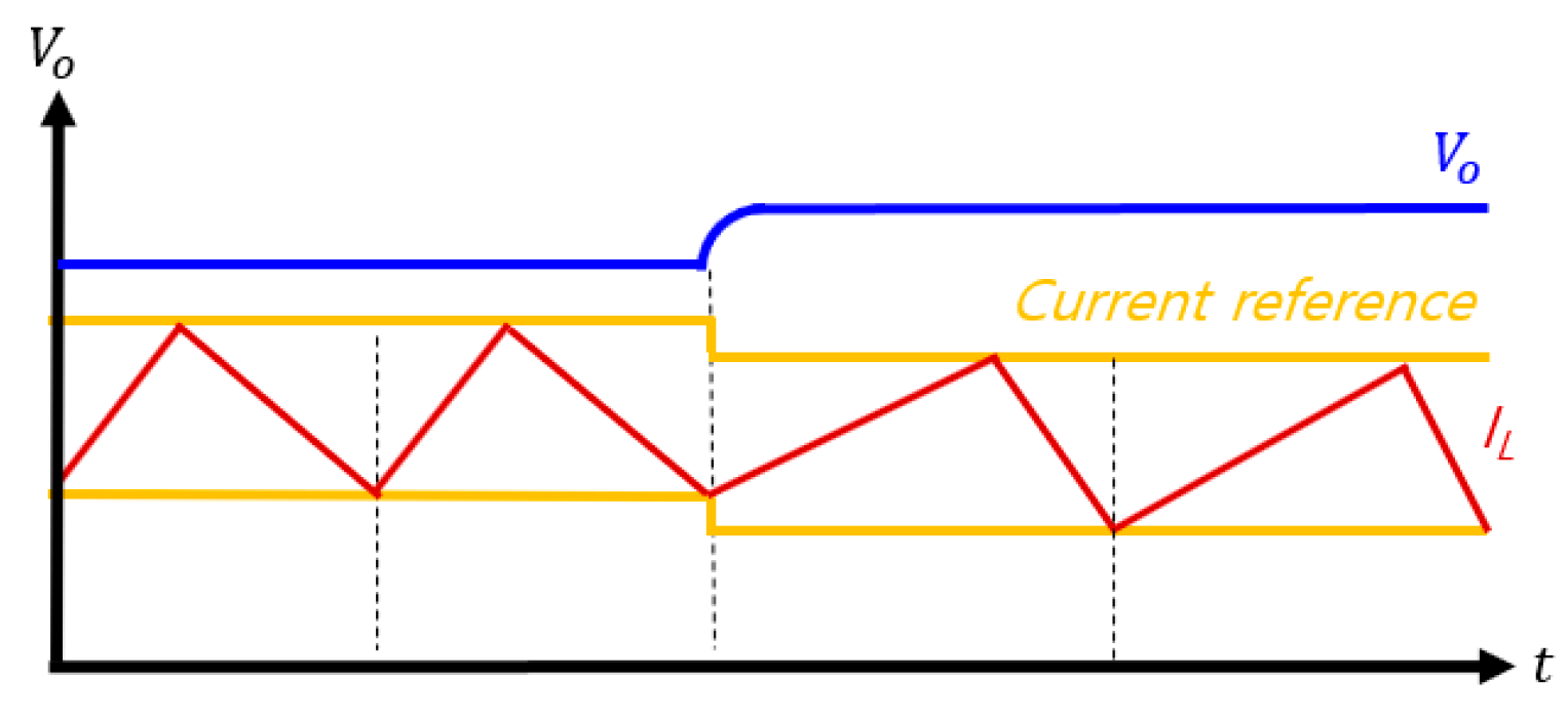
3.1. Features of Valley Current Mode Control

Typically, current mode control methods include: average current mode control, peak current mode control, and valley current mode control [20,21,22]. Figure 11 shows a block diagram of valley current mode control. In contrast to peak current mode control, valley current mode control turns the transistor off at regular intervals in the clock pulse, which is the reset signal. In addition, when the inductor current and the minimum current command signal become equal, a set signal is generated, and the transistor is turned on. However, in the case of the valley current mode control method, in contrast to peak current mode control, sub-harmonic oscillation occurs when the duty cycle is less than 0.5 [23]. Figure 12 shows the current waveform of the valley current mode control formed according to the operation shown in Figure 11. As shown in the figure, when the duty cycle is above 0.5, the magnitude of the current perturbation becomes small and sub-harmonic oscillation does not occur.

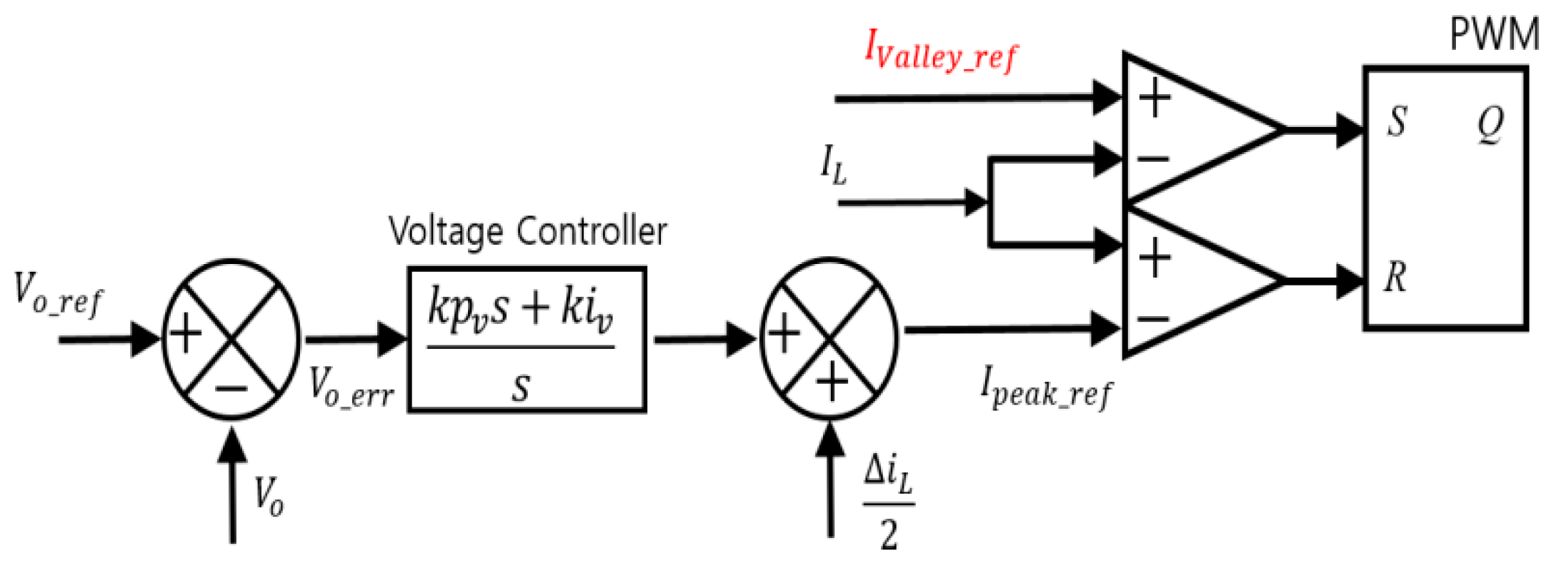
3.2. The Proposed Hybrid Current Mode Control
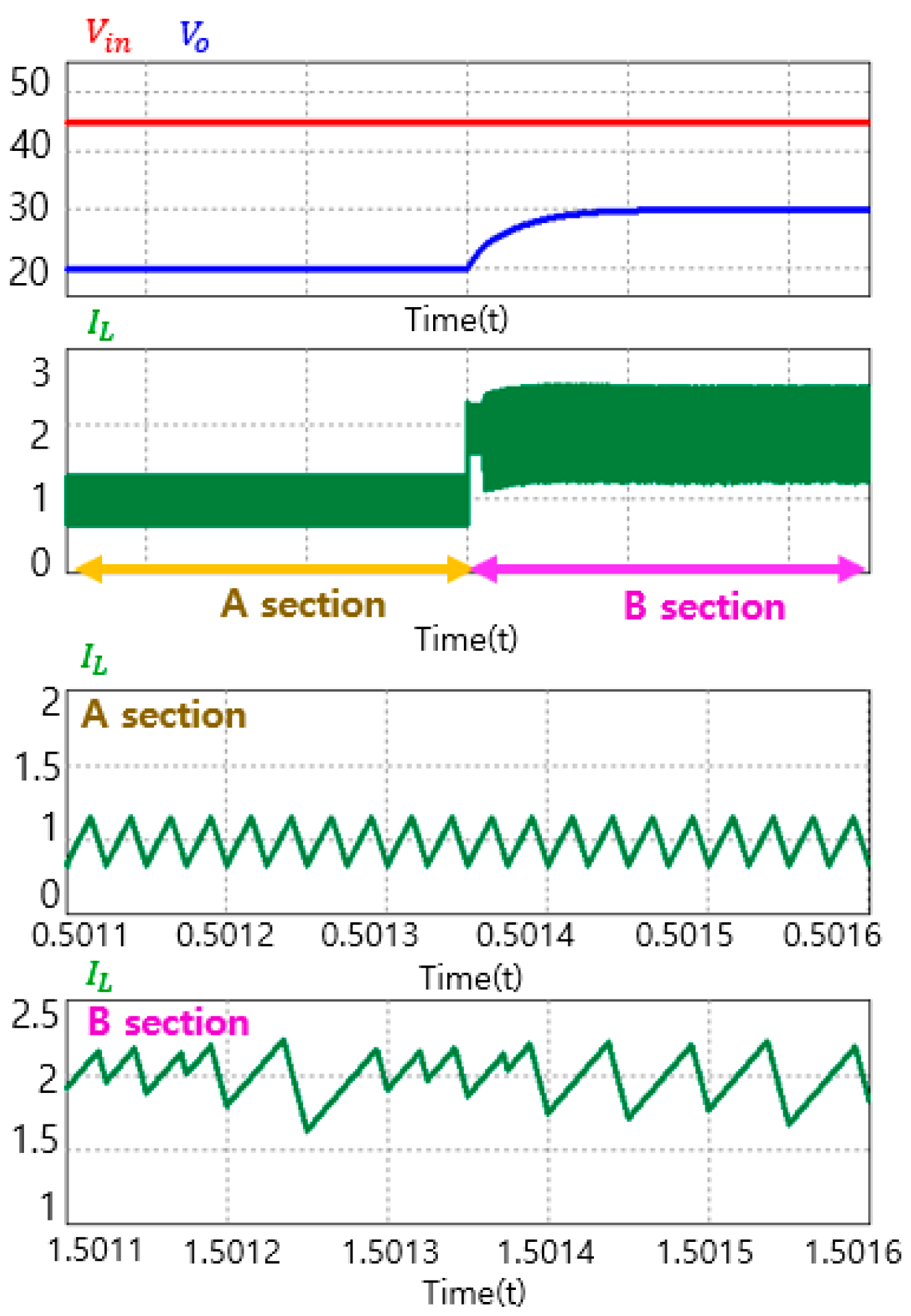
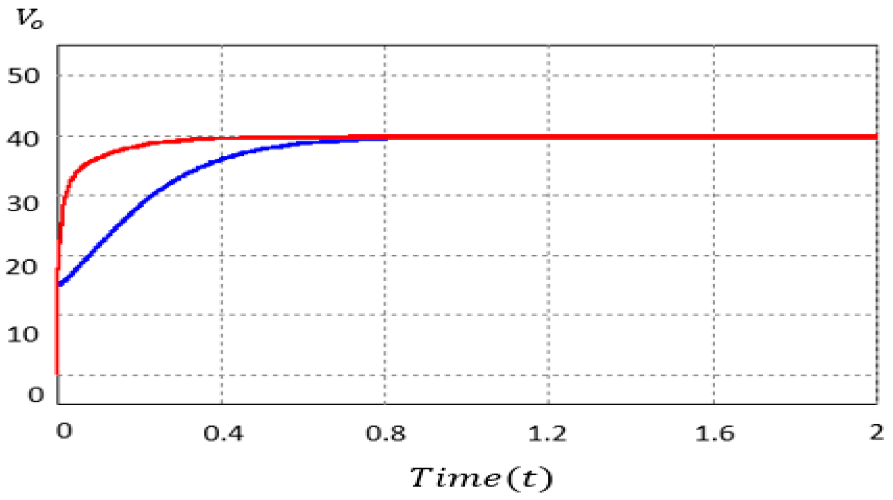
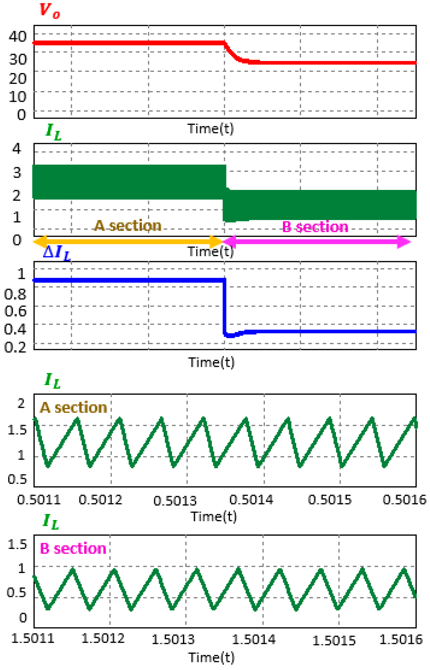
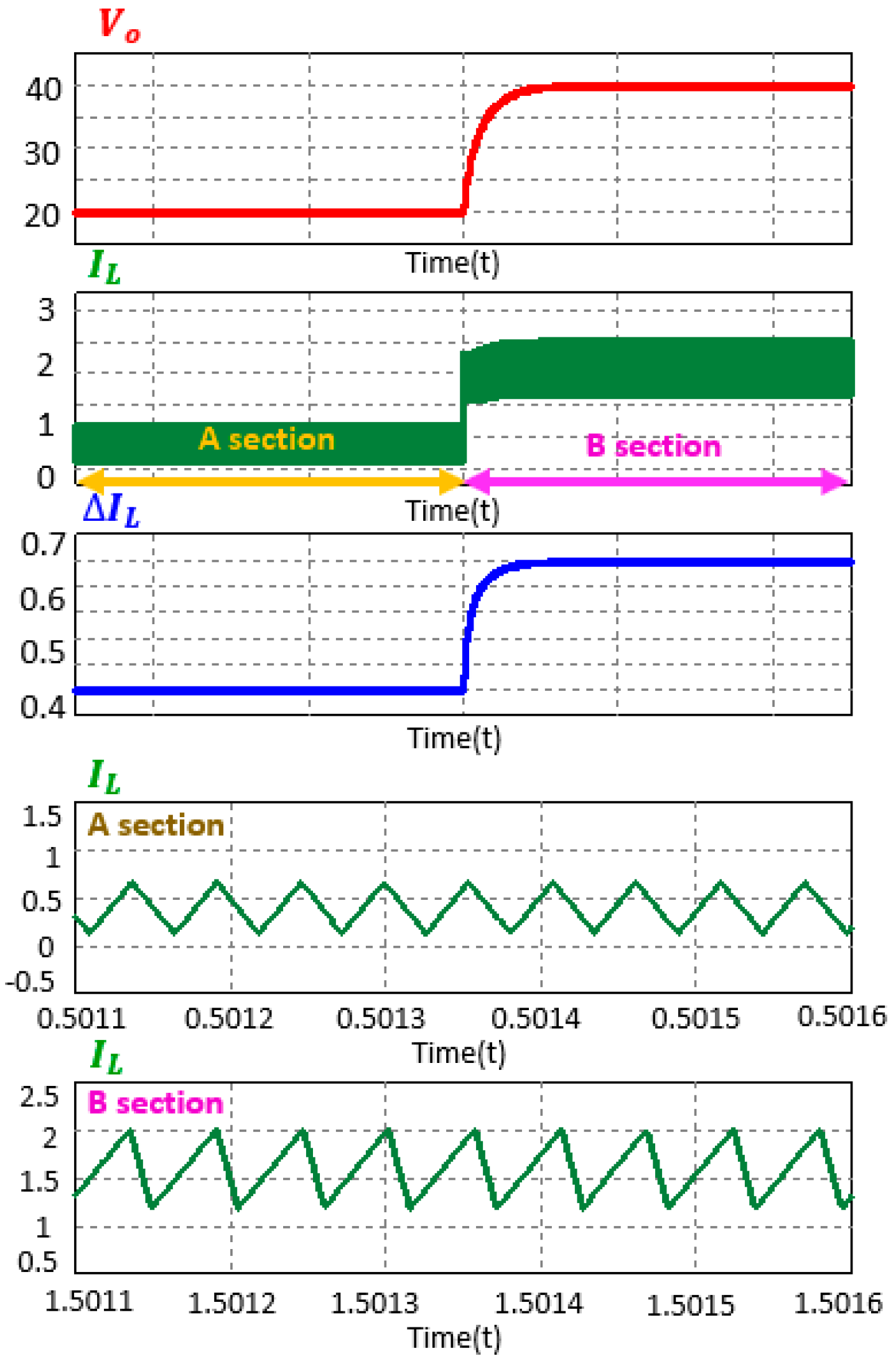
In this paper, a new hybrid current mode controller is proposed, using both maximum and minimum currents. The proposed hybrid current controller is similar to the hysteretic current mode controller. Previous hysteresis current-mode control methods make use of a fixed band-gap [24,25,26,27]. In this case, the frequency will fluctuate when the input voltage and the output voltage change, which can be due to the thermal stress of the power device and can cause the efficiency of the controller to decrease for certain input and output voltage conditions. On the other hand, the hybrid current mode control proposed in this paper changes the current band gap organically to fix the switching frequency even if the input and output voltages change.
In order to operate at a constant frequency irrespective of the input/output voltage conditions, the relationship between the input/output voltage condition and the current band gap should be known. Figure 13 shows the steady-state inductor current waveform. In Figure 13, m1 represents the rising slope of the inductor current, and DT represents the time at which the inductor current rises. The current band gap ( I L ) is given by Equation (10), where f is the PWM frequency. In Equation (10), the current band gap ( I L ) is the product of the rising current slope and the rising time.
Therefore, the current band gap is changed by the rising current slope as shown in Equation (10), which is the input/output voltage and frequency function. The newly obtained maximum current command is then obtained as shown in Equation (11), and the minimum current command is calculated as shown in Equation (12), by subtracting the current bandgap from the maximum current command:
I L = m 1 × D T = V g × D T L = V g × ( V o V g ) L × V g × f
I L p e a k _ r e f = I L A v g _ r e f + I L 2
I L v a l l e y _ r e f = I L p e a k _ r e f I L
Here, I L A v g _ r e f is an average current command signal derived from the voltage controller. Figure 14 shows a proposed hybrid current mode control block diagram derived using the newly obtained minimum current.
It can be seen that the inductor current is compared to the maximum and minimum current command signals. The difference between the previous method shown in Figure 1 and the proposed method shown in Figure 14 can be described as follows: in a previous paper [19], two slopes were used at the top and bottom to eliminate sub-harmonic oscillation. Since the slope of the top and bottom is affected by the input and output voltages, the slope must also be modified and changed by the changing input and output voltages. However, it is difficult to periodically change the slope initially set in hardware. In the proposed controller, the slope is used to select the band-gap in software as shown in Equation (10). Therefore, the slope of the proposed controller has the advantage of changing and adapting itself to fix the frequency when the input and output voltages are changed. Figure 15 shows the control waveform of the proposed controller when the output voltage fluctuates. When the input/output voltages are changed, the current band-gap is also changed at the same time, hence, fixing the frequency without changing.

4. Simulation

A simulation analysis was conducted to compare peak current mode control using conventional slope compensation and using the proposed hybrid current mode control. Table 1 shows the parameters of the boost converter for simulated analysis. The input voltage is 10 V, the maximum output voltage is 50 V, the switching frequency is 20 kHz, and the maximum slope is set to 80 k. The simulation was performed using the PSIM Tool and a boost converter was constructed as shown in Figure 16. In addition, the peak current mode controller-set to use the maximum slope-and the proposed hybrid current mode controller were compared and analyzed using two different controllers.
Figure 17 shows the output voltage waveforms of the peak current mode control, including the maximum slope compensation method and the proposed hybrid current mode control. When the maximum slope was used, a time-delay problem was introduced, because the compensation was greater than the original compensation value. On the other hand, the proposed hybrid current mode controller had a faster response time. Thus, the voltage control had a quick response characteristic.
Figure 18 and Figure 19 show the inductor current waveform when the output voltage is lowered and raised, respectively, using the proposed hybrid current mode control. Section A is the inductor current waveform before the output voltage changes from high to low and Section B shows the inductor current waveform after the output voltage changes from high to low. It can also be confirmed that the current bandwidth changes with changing input/output voltage. Existing conventional hysteresis current mode control makes use of a fixed band gap, which causes the frequency to fluctuate when the output voltage is changed. However, since the proposed hybrid current mode control changes the current bandwidth at the same time that the output voltage changes, it can be seen that the controller operates stably without changing frequency.

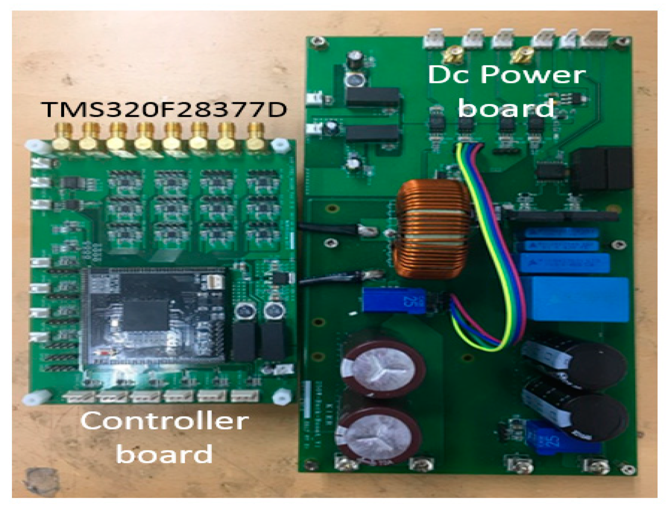
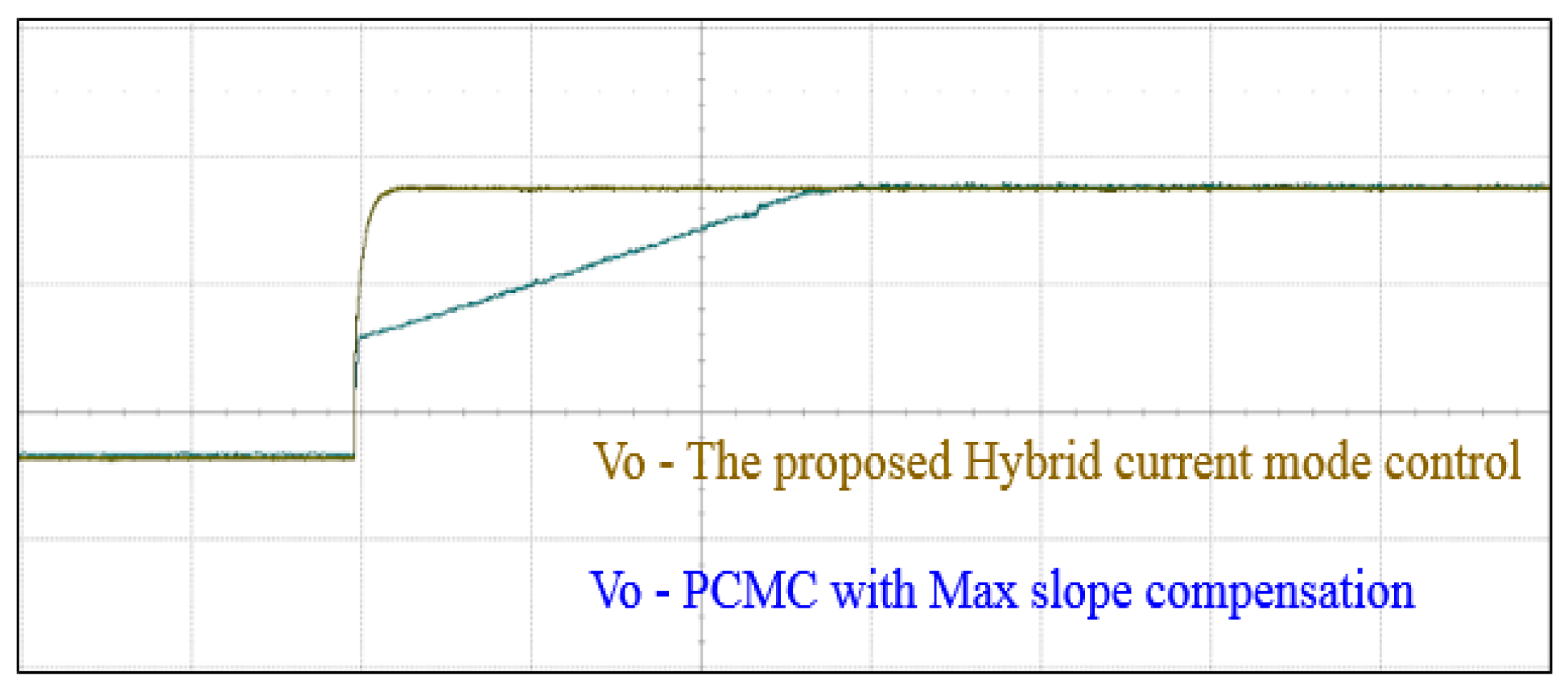
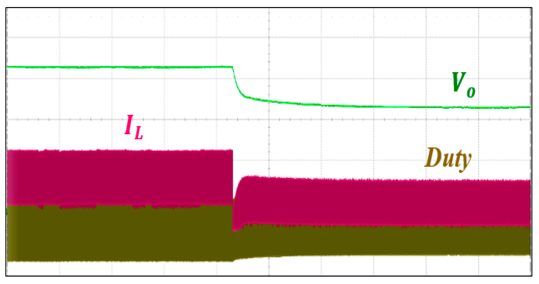
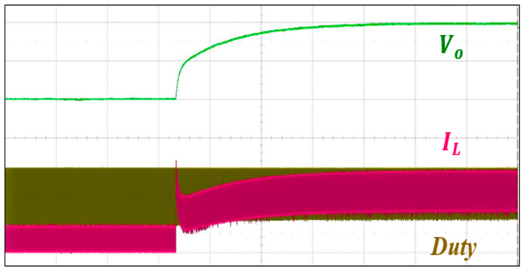
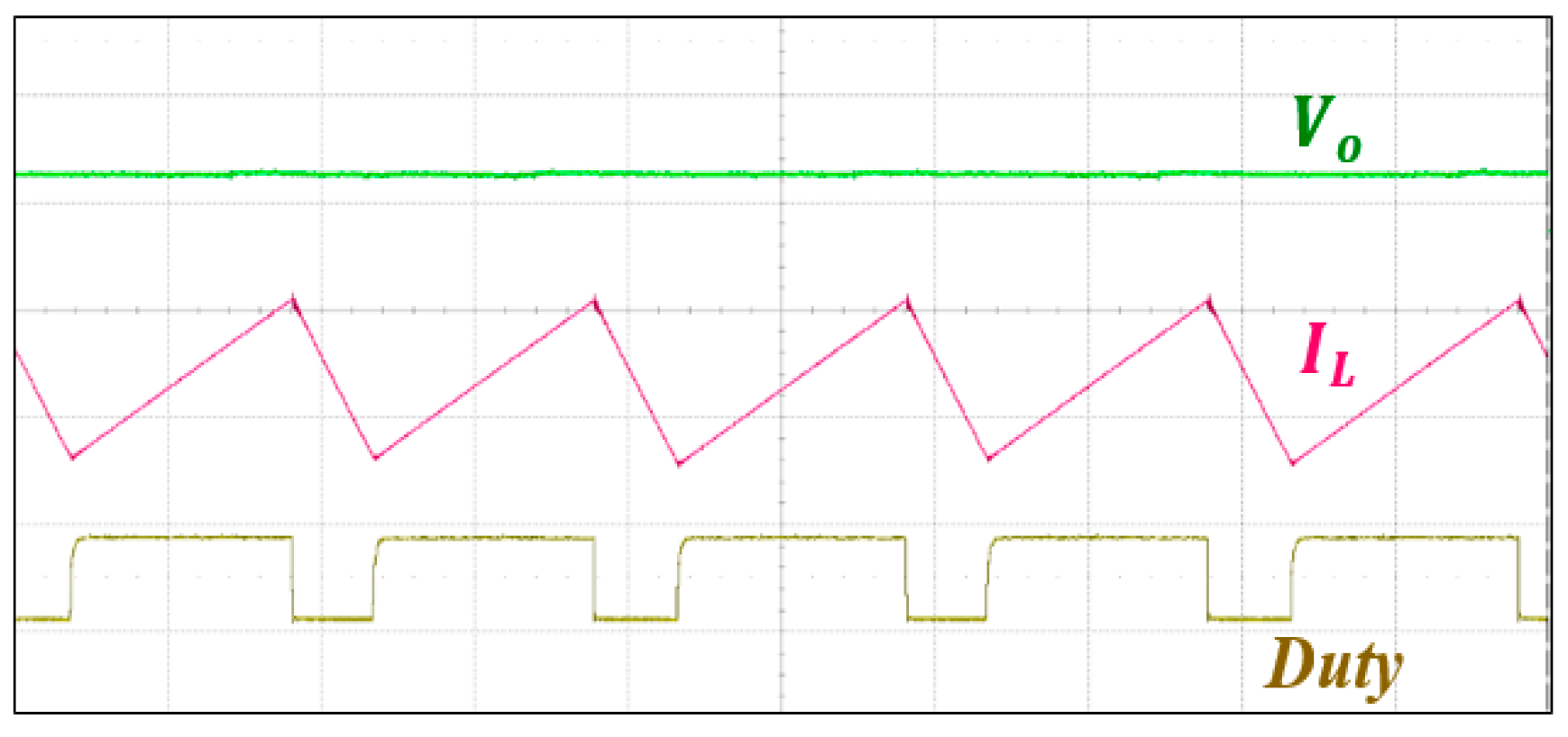
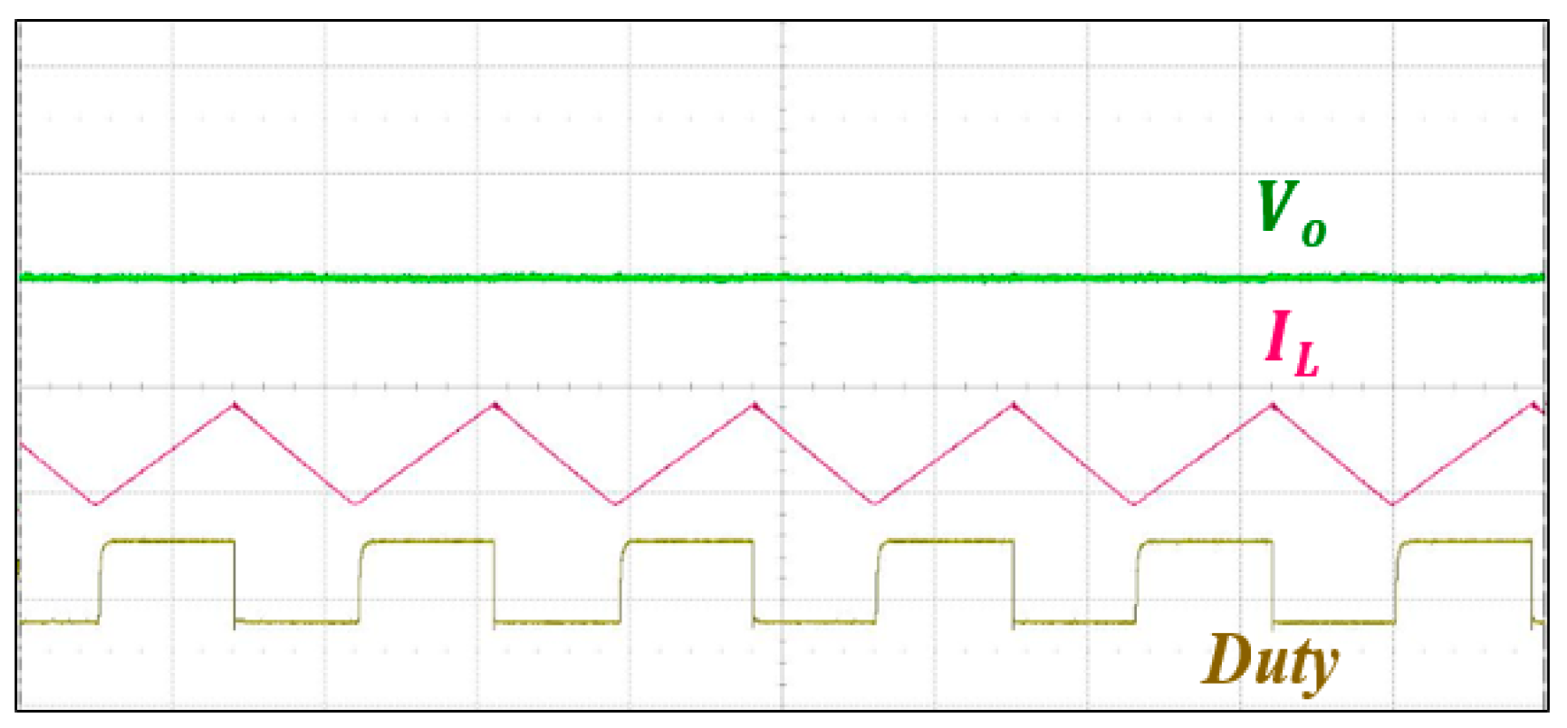
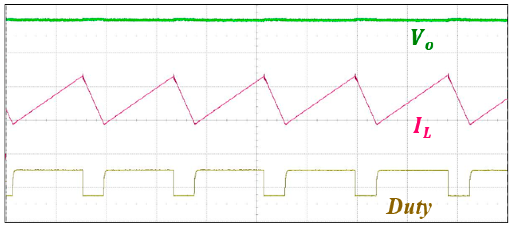
5. Experimental Results

Figure 20 shows the experimental setup for a single-phase boost converter to verify the proposed hybrid current mode control. The experimental equipment consisted of a DC power board and a controller board. The experiment proceeded using the same parameters as the simulation analysis. To control the MCU, theTMS320F28377D microcontroller from Texas Instruments (Dallas, TX, USA) was used for digital control. Figure 21 shows a digital controller implementation of the hybrid current mode control. The proposed hybrid current mode digital controller functions as follows: when the inductor current reached the maximum current command signal, the maximum current command was changed to the minimum current command and the transistor was turned off. When the inductor current reached the minimum current command signal, the minimum current command was changed to the maximum current command and the transistor was turned on. Figure 22 shows the output voltage waveforms of the peak current mode control. Plots of both the maximum slope compensation method and the proposed hybrid current mode control are shown on the same set of axes.
It can be seen that the proposed hybrid current mode control has faster response characteristics, as shown before in the simulation analysis. Figure 23 and Figure 24 show the inductor current waveform of the proposed hybrid current mode control when the output voltage was lowered and raised, respectively. The input voltage was changed from 35 V to 25 V and the output voltage was changed from 20 V to 40 V. Figure 25 and Figure 26 show the inductor current waveform before the output voltage rose and dropped, respectively. Figure 27 and Figure 28 show the inductor current waveform after the output voltage rose and dropped, respectively. It can be confirmed that the frequency was fixed as in the simulation analysis.

6. Conclusions

In this paper, a new hybrid current mode controller was proposed and studied with fast response characteristics for high-speed charging and discharging of energy storage devices that incorporate a super capacitor. Typically, for fast response characteristics, peak current mode control and slope compensation methods are used. When the voltage suddenly changes, the slope value is typically set to the maximum, which causes a response time delay. Through simulation and experimental analysis, it was confirmed that the proposed hybrid current mode controller had faster response characteristics than the peak current mode controller using maximum slope compensation. In addition, it was confirmed that when the output voltage was changed, the frequency did not change and the controller operated stably.

Author Contributions

S.-M.O. implemented the system and performed the experiments. H.-W.K. provided the idea and managed the paper. J.-h.K. and K.-Y.C. assisted in idea development and paper writing.

Funding

This work was supported by the Industrial Strategic Technology Development Program (KEIT) funded By the Ministry of Trade, Industry & Energy (MOTIE) of the Republic of Korea (No. 201801180001). This work was supported by “Human Resources Program in Energy Technology” of the Korea Institute of Energy Technology Evaluation and Planning (KETEP), granted financial resource from the Ministry of Trade, Industry & Energy, Republic of Korea (No. 20184030202270).

Conflicts of Interest

The authors declare no conflict of interest.

References

  1. Lianfu, T.; Lixin, W. Research on the Integrated Braking Energy Recovery Strategy Based on Super-Capacitor Energy Storage. In Proceedings of the 2017 International Conference on Smart Grid and Electrical Automation (ICSGEA), Changsha, China, 27–28 May 2017; pp. 175–178. [Google Scholar]
  2. Lin, S.; Song, W.; Luo, L.; Lv, J.; Feng, Z. Research on the capacity of hybrid energy storage system and its control method in rail transit traction grid. In Proceedings of the 2015 International Conference on Smart Grid and Clean Energy Technologies (ICSGCE), Offenburg, Germany, 20–23 October 2015; pp. 103–106. [Google Scholar]
  3. Wang, L.; Zou, T.; Lin, X. A novel control strategy for doubly fed induction generator in micro-grid with super capacitors. In Proceedings of the 2011 International Conference on Electrical and Control Engineering, Yichang, China, 16–18 September 2011; pp. 3788–3791. [Google Scholar]
  4. Kong, S.J.; Yang, T.C.; Kang, K.S.; Roh, C.W. Capacitor Bank Assisted Battery Fed Boost Converter for Self-electricity-generated Transportation Cart System. Trans. Korean Inst. Power Electron. 2018, 23, 1–8. [Google Scholar]
  5. Lin, K.; Lian, K. Actual measurement on regenerative elevator drive and energy saving benefits. In Proceedings of the 2017 International Automatic Control Conference (CACS), Pingtung, Taiwan, 12–15 November 2017; pp. 1–5. [Google Scholar]
  6. Chen, Q.-Z.; Ma, W.-B.; Chen, X.-F. Research on the lead-acid battery and ultra-capacitor energy storing system of motor vehicles regenerative braking. In Proceedings of the 2012 IEEE International Conference on Computer Science and Automation Engineering (CSAE), Zhangjiajie, China, 25–27 May 2012; pp. 59–62. [Google Scholar]
  7. Furukawa, Y.; Nibu, S.; Colak, I.; Eto, H.; Kurokawa, F. Transient response of digital peak current mode boost converter for DC bus voltage compensation. In Proceedings of the 2016 IEEE International Conference on Renewable Energy Research and Applications (ICRERA), Birmingham, UK, 20–23 November 2016; pp. 809–812. [Google Scholar]
  8. Kajiwara, K.; Maruta, H.; Shibata, Y.; Matsui, N.; Kurokawa, F.; Hirose, K. Wide input digital peak current mode DC-DC converter for DC power feeding system. In Proceedings of the 2016 IEEE International Telecommunications Energy Conference (INTELEC), Austin, TX, USA, 23–27 October 2016; pp. 1–4. [Google Scholar]
  9. Furukawa, Y.; Maeda, S.; Kurokawa, F.; Colak, I. Performance characteristic of digital peak current mode control switching power supply. In Proceedings of the 2015 17th European Conference on Power Electronics and Applications (EPE’15 ECCE-Europe), Geneva, Switzerland, 8–10 September 2015; pp. 1–10. [Google Scholar]
  10. Furukawa, Y.; Nibu, S.; Kurokawa, F.; Colak, I. Improving stability of switching power supply with digital peak current mode control. In Proceedings of the 2016 IEEE International Conference on Renewable Energy Research and Applications (ICRERA), Birmingham, UK, 20–23 November 2016; pp. 952–955. [Google Scholar]
  11. Abe, S.; Shoyama, M.; Ninomiya, T. First-order transient response of DC-DC converter with peak current mode control for low-voltage application. In Proceedings of the 2008 International Symposium on Power Electronics, Electrical Drives, Automation and Motion, Ischia, Italy, 11–13 June 2008; pp. 32–36. [Google Scholar]
  12. Lee, J.U.; Kim, H.W.; Baek, S.W.; Cho, K.Y. Current Reference Compensation for Fast Response in PCMC of PSFB Converter. Trans. Korean Inst. Power Electron. 2018, 23, 147–151. [Google Scholar]
  13. Sundaramoorthi, S.; Karunanithi, K.; Saravanan, S.; Praveenkumar, S. Investigation and control of chaos in DC-DC noel converter using slope compensation method. In Proceedings of the 2017 IEEE International Conference on Intelligent Techniques in Control, Optimization and Signal Processing (INCOS), Srivilliputhur, India, 23–25 March 2017; pp. 1–5. [Google Scholar]
  14. Chen, J.; Hwang, Y.; Hwang, B.; Jhang, Y.; Ku, Y. A dual-mode fast-transient average-current-mode buck converter without slope-compensation. In Proceedings of the 2018 7th International Symposium on Next Generation Electronics (ISNE), Taipei, Taiwan, 7–9 May 2018; pp. 1–4. [Google Scholar]
  15. Yang, Y.; Lu, W.; Iu, H.H.C.; Fernando, T. Stabilization of fast-scale instabilities in PCM boost PFC converter with dynamic slope compensation. In Proceedings of the 2015 IEEE International Symposium on Circuits and Systems (ISCAS), Lisbon, Portugal, 24–27 May 2015; pp. 2481–2484. [Google Scholar]
  16. Min, B.S.; Park, N.J.; Hyun, D.S. A Novel Current Sharing Technique for Interleaved Boost Converter. Trans. Korean Inst. Power Electron. 2007, 12, 165–173. [Google Scholar]
  17. Jianan, W. Improved delay-dependent stability criteria for linear system with interval time-varying delay. In Proceedings of the 31st Chinese Control Conference, Hefei, China, 25–27 July 2012; pp. 1325–1329. [Google Scholar]
  18. Hulea, D.; Muntean, N.; Cornea, O. Valley current mode control of a bi-directional hybrid DC-DC converter. In Proceedings of the 2015 International Aegean Conference on Electrical Machines &Power Electronics (ACEMP), 2015 International Conference on Optimization of Electrical &Electronic Equipment (OPTIM) &2015 Intl Symposium on Advanced Electromechanical Motion Systems (ELECTROMOTION), Side, Turkey, 2–4 September 2015; pp. 274–279. [Google Scholar]
  19. Kapat, S. Parameter-Insensitive Mixed-Signal Hysteresis-Band Current Control for Point-of-Load Converters with Fixed Frequency and Robust Stability. IEEE Trans. Power Electron. 2017, 32, 5760–5770. [Google Scholar] [CrossRef]
  20. Park, H.C.; Kim, I.S. Average Current Mode Control Technique Having Fast Response. Trans. Korean Inst. Power Electron. 2017, 22, 231–239. [Google Scholar]
  21. Zhou, G.; Xu, J.; Mi, C.; Jin, Y. Effects of modulations on the sub-harmonic oscillations of digital peak current and digital valley current controlled switching DC-DC converters. In Proceedings of the 2009 IEEE 6th International Power Electronics and Motion Control Conference, Wuhan, China, 17–20 May 2009; pp. 1347–1352. [Google Scholar]
  22. Mohamed, E.E.M.; Sayed, M.A.; Mohamed, T.H. Sliding mode control of linear induction motors using space vector controlled inverter. In Proceedings of the 2013 International Conference on Renewable Energy Research and Applications (ICRERA), Madrid, Spain, 20–23 October 2013; pp. 650–655. [Google Scholar]
  23. Farah, N.; Talib, M.H.N.; Ibrahim, Z.; Isa, S.N.M.; Lazi, J.M. Variable hysteresis current controller with fuzzy logic controller based induction motor drives. In Proceedings of the 2017 7th IEEE International Conference on System Engineering and Technology (ICSET), Shah Alam, Malaysia, 2–3 October 2017; pp. 122–127. [Google Scholar]
  24. Awasthi, A.; Patel, D. Implementation of adaptive hysteresis current control technique for shunt active power conditioner and its comparison with conventional hysteresis current control technique. In Proceedings of the 2017 IEEE International Conference on Signal Processing, Informatics, Communication and Energy Systems (SPICES), Kollam, India, 8–10 August 2017; pp. 1–6. [Google Scholar]
  25. Linca, M.; Suru, C.V.; Preda, C.A. Indirect Current Control Algorithm Implementation for an Active Filtering System Using Constant Switching Frequency Hysteresis Controllers. In Proceedings of the 2018 International Conference on Applied and Theoretical Electricity (ICATE), Craiova, Romania, 4–6 October 2018; pp. 1–6. [Google Scholar]
  26. Duong, V.H.; Tran, N.-T.; Park, Y.J.; Choi, W.J. Novel Estimation Technique for the State-of-Charge of the Lead-Acid Battery by using EKF Considering Diffusion and Hysteresis Phenomenon. Trans. Korean Inst. Power Electron. 2014, 19, 139–148. [Google Scholar] [CrossRef] [Green Version]
  27. Loh, P.; Bode, G.; Homes, D.; Lipo, T. A Time-Based Double-Band Hysteresis Current Regulation Strategy for Single-PhaseMultilevel Inverters. IEEE Trans. Ind. Appl. 2003, 39, 883–892. [Google Scholar]
Figure 1. Previousmethod for preventing the sub-harmonic oscillation problem.
Electronics 08 00112 g001
Figure 2. Operation principle of peak current mode control.
Electronics 08 00112 g002
Figure 3. Waveforms with slope compensation at ideal current and sub-harmonic oscillation current.
Electronics 08 00112 g003
Figure 4. Comparison between ideal current and slope compensation.
Electronics 08 00112 g004
Figure 5. Comparison between sub-harmonic oscillation current and slope compensation.
Electronics 08 00112 g005
Figure 6. Comparison between ideal current and slope compensation.
Electronics 08 00112 g006
Figure 7. Comparison between sub-harmonic oscillation current and slope compensation.
Electronics 08 00112 g007
Figure 8. Inductor current waveform for changing input voltage.
Electronics 08 00112 g008
Figure 9. Inductor current waveform for changing output voltage.
Electronics 08 00112 g009
Figure 10. Duty cycle using different slopes.
Electronics 08 00112 g010
Figure 11. Block diagram of Valley current mode control.
Electronics 08 00112 g011
Figure 12. Inductor current that occurs when duty is above 0.5 in Valley current mode control.
Electronics 08 00112 g012
Figure 13. Steady-state inductor current.
Electronics 08 00112 g013
Figure 14. Proposed hybrid current mode control block diagram.
Electronics 08 00112 g014
Figure 15. Inductor current due to changing output voltage.
Electronics 08 00112 g015
Figure 16. Boost converter circuit in Powersim (PSIM) simulation.
Electronics 08 00112 g016
Figure 17. Response time for different controllers.
Electronics 08 00112 g017
Figure 18. Proposed hybrid current mode controller inductor current response to a lowered output voltage.
Electronics 08 00112 g018
Figure 19. Proposed hybrid current mode controller inductor current response to a rise in output voltage.
Electronics 08 00112 g019
Figure 20. Experimental setup with boost converter.
Electronics 08 00112 g020
Figure 21. A waveform that implements a digital controller.
Electronics 08 00112 g021
Figure 22. Response time for different controllers. (20 V/div, 400 ms/div).
Electronics 08 00112 g022
Figure 23. Inductor current waveform when the output voltage is lowered in the proposed hybrid current mode control. (10 V/div, 1 A/div, 50 ms/div).
Electronics 08 00112 g023
Figure 24. Inductor current waveform when the output voltage is raised in the proposed hybrid current mode control. (10 V/div, 1 A/div, 50 ms/div).
Electronics 08 00112 g024
Figure 25. Inductor current waveform before a drop in output voltage. (10 V/div, 1 A/div, 25 us/div).
Electronics 08 00112 g025
Figure 26. Inductor current waveform after a drop in output voltage. (10 V/div, 1A/div, 25 us/div).
Electronics 08 00112 g026
Figure 27. Inductor current waveform before a rise in output voltage. (10 V/div, 1A/div, 25 us/div).
Electronics 08 00112 g027
Figure 28. Inductor current waveform after a rise in output voltage. (10 V/div, 1A/div, 25 us/div).
Electronics 08 00112 g028
Table 1. System parameters.
ParameterValue
Input Voltage10 (V)
Output Voltage50 (V)
Inductor500 (uH)
capacitor440 (uF)
Max slope80 k
Switch frequency20 (kHz)

