Article

Line Frequency Instability of One-Cycle-Controlled Boost Power Factor Correction Converter

1
College of Safety Engineering, Chongqing University of Science and Technology, Chongqing 401331, China
2
College of Electrical Engineering, Chongqing University of Science and Technology, Chongqing 401331, China
3
The School of Electric Power Engineering, South China University of Technology, Guangzhou 510641, China
4
Department of Electrical Egineering, Chongqing Institute of Communication, Chongqing 400035, China
*
Authors to whom correspondence should be addressed.
Electronics 2018, 7(9), 203; https://doi.org/10.3390/electronics7090203
Submission received: 26 July 2018 / Revised: 30 August 2018 / Accepted: 4 September 2018 / Published: 17 September 2018
(This article belongs to the Special Issue Applications of Power Electronics)

Abstract

:
Power Factor Correction (PFC) converters are widely used in engineering. A classical PFC control circuit employs two complicated feedback control loops and a multiplier, while the One-Cycle-Controlled (OCC) PFC converter has a simple control circuit. In OCC PFC converters, the voltage loop is implemented with a PID control and the multiplier is not needed. Although linear theory is used in designing the OCC PFC converter control circuit, it cannot be used in predicting non-linear phenomena in the converter. In this paper, a non-linear model of the OCC PFC Boost converter is proposed based on the double averaging method. The line frequency instability of the converter is predicted by studying the DC component, the first harmonic component and the second harmonic component of the main circuit and the control circuit. The effect of the input voltage and the output capacitance on the stability of the converter is studied. The correctness of the proposed model is verified with numerical simulations and experimental measurements.

1. Introduction

Power Factor Correction (PFC) plays an important role in electrical engineering [1]. A PFC converter takes AC voltage as its input and outputs DC voltage. Different from traditional diode rectifiers, a PFC converter in average current mode has a high power factor. In electrical engineering, the average current mode Boost PFC converter is widely used. Although the topology of the Boost PFC is simple, the control circuit is complicated [2,3,4]. The control circuit consists of two loops. The first is the current control loop, with the aim of forcing the inductor current to be in the same phase as the reference. The second loop is the voltage control loop. The design of the voltage control loop is of great importance because its main objective is achieving a stable system and a near unity power factor [4]. The dynamics of the PFC converter depends on these two control loops. The traditional implementation for the PFC converter requires a multiplier, whose output is the reference current added to the current control loop. The existence of the multiplier increases the control complexity. The dynamics of the PFC converter has interested many researchers and some non-linear phenomena have been observed in the last few years [5,6,7,8,9,10,11,12,13]. In general, there are two kinds of non-linear dynamics in the PFC converter. The first is the so-called switching frequency instability, which is mainly the result of bifurcation and chaos caused by the current control loop [5]. The second is the line frequency instability, which is the result of bifurcation and chaos caused by the voltage control loop [7,8,9,10,11,14]. Among them, the line frequency instabilities are more detrimental to the normal operation of the PFC converter, as it changes the power factor to an unacceptable value. The power factor of the converter is much less than one due to the line frequency instabilities and thus, it is of great importance to select the appropriate parameters in the design process. In the traditional design, the researchers adopted the linear system theory and it has been shown that this design cannot predict the line frequency instabilities in the PFC converter [7]. Therefore, the researchers developed some powerful methods to compute the boundaries of line frequency stabilities. Among them, the method of harmonic balance needs an exact computation of the unstable periodic orbit of the control voltage [9]. Harmonic balance is applied to the model of the converter incorporating the multiplier and Floquet theory is adopted to decide the stability of the converter. According to Floquet theory, the stability of the converter is identified by calculating the eigenvalues of the transition matrix of the system. Another important method is the method of double averaging, which is based on the first harmonic component in the PFC converter line frequency model [14]. This method is more familiar to many researchers and engineers. In this paper, the later method is adopted to study the non-linear dynamics of the continuous conduction mode One-Cycle-Controlled (OCC) Boost PFC converter.
Different from the traditional average current mode PFC converter, the OCC PFC converter simplifies the control circuit [3]. The one-cycle control belongs to non-linear controls. When this control method is applied to the PFC converter, the current control loop is replaced by a resettable integrator. Therefore, only one voltage control loop is required and the multiplier is not needed. It has been shown that the control circuit of the OCC Boost PFC converter saves space and cost compared to the traditional PFC Boost converter. In most applications, the voltage control loop is designed based on the linear system theory and the prediction of dynamics of the converter is also based on the linear system theory. Therefore, non-linear dynamics of the converter are uncovered. In many applications, bifurcation and chaos are observed but are not addressed. The reason is that the non-linear systems theory is not applied to the OCC PFC converter. In this paper, the method of double averaging is adopted to predict the non-linear dynamics of the OCC Boost PFC converter. Although this method has been applied to the traditional PFC converter, there is still a problem when applying it to the OCC PFC converter, because the control circuits in the two converters are totally different and as a result, some new consequences will occur in the OCC PFC converter. It is important to note that in a previous study [15], the non-linear dynamics of the OCC PFC converter were observed by experiments and no effective computation was provided. In the present paper, the computation is based on the exact non-linear model of the OCC PFC converter and therefore, the conclusions are meaningful in the design process of the converter.

2. The OCC Boost PFC Converter

2.1. The OCC Boost PFC Converter and Its Control Circuit

The OCC Boost PFC converter consists of a diode rectifier and a boost converter, as shown in Figure 1. In some applications, the load of the PFC converter is another DC-DC converter. In this paper, the load of the PFC converter is a resistor, because the emphasis of this paper is on the non-linear dynamics of the PFC converter. The control circuit in Figure 1 is equivalent to a commercial control IC IR1150, which is used to verify the theoretical results in this paper. Apparently, this control circuit has fewer resistors and capacitors than the traditional average current mode PFC converter, where both the current loop and the voltage loop have at least one resistor and one capacitor. The output of the converter is divided by R f 1 and R f 2 . The divided voltage is connected to the input of an Operational Amplifier (OA), whose other input is the reference V r e f . In IR1150, the OA is a trans-conductance type amplifier. The output of the OA is v m , which is the input to a resettable integrator. The output of the integrator is compared with another voltage composed of v m and the voltage across the current sense resistor R s 1 . The integrator is reset by the output Q ¯ of the flip-flop. The sensed voltage is amplified by a DC gain G D C = 2.5 . The operation of the control circuit is described here. In the beginning of every switching period T s , the clock sets the flip-flop and the output Q of the flip-flop turns on the switch S. At the same time, the integrator outputs the value of the integral of its input signal. When the output of the integrator exceeds the sum of v m and the sensed voltage, the comparator resets the flip-flop and the output Q turns off the switch S. Therefore, the diode D turns on. Furthermore, the output Q ¯ resets the integrator until the next clock signal.

2.2. The OCC Boost PFC Converter Model

In this paper, the line frequency dynamics are studied. Therefore, the method of double averaging is adopted. The method is composed of two averaging processes. The first averaging is applied to the switching period [16,17,18,19,20,21,22]. The converter has two topology structures during one switching period, and is described by:
{ d i L d t = 1 L v i n d v o d t = 1 R C v o ( the   switch   S   is   on )   or   { d i L d t = 1 L ( v i n v o ) d v o d t = 1 C ( i L v o R )   ( the   switch   S   is   off ) .
By averaging over one switching period, one obtains the following:
{ ( 1 d ) v o = v i n L d i L d t ( 1 d ) i L = C d v o d t + v o R .
From Equation (2), we obtain:
C 2 d v o 2 d t = v 0 2 R + i L v i n L 2 d i L 2 d t .
It is important to note that the dynamics of the inductor during one switching period can be omitted when the converter operates stably. Therefore, one has
C 2 d v o 2 d t = v 0 2 R + i L v i n .
Based on the operating principle of the converter [3,4,5,6,7,8], one has:
R s i L ( t ) = v m / T ( d ) ,
where:
T ( d ) = v o / v i n ,   R s = R s 1 × 2.5  
From Equations (5) and (6), we can obtain:
i L ( t ) = v i n v m / ( R s v o ) .
It is important to note that v i n = V m | sin ω m t | . Substituting Equation (7) into (4), we obtain:
C 2 d v o 2 d t = v 0 2 R + v m R s v o V m 2 ( 1 cos 2 ω m t ) .
On the other hand, the control loop includes the OA. Figure 1 provides the following transfer function of the OA:
H ( s ) = g m ( 1 + s R g m C z ) s ( C z + C p + s R g m C z C p ) .
As C z C p , Equation (9) can be written as:
H ( s ) = g m ( 1 + s R g m C z ) s C z .
Therefore, the voltage control loop in Figure 1 is described by:
C z d v m d t = g m ( V r e f R f 2 R f 1 + R f 2 v o ) g m R g m C z R f 2 R f 1 + R f 2 d v o d t ,
where g m is the trans-conductance of the amplifier.
From Figure 1, one has:
i L ( t ) = v i n v m R f 2 R s ( R f 1 + R f 2 ) V r e f .
Therefore, the OCC Boost PFC converter is described by:
{ C 2 d x 2 d t = x 2 R + y R s ( 1 + β ) V r e f V m 2 ( 1 cos 2 ω m t ) C z d y d t = g m ( V r e f 1 1 + β x ) g m R g m C z 1 1 + β d x d t ,
where v m = y , v o = x , β = R f 1 / R f 2 .
The next step is applying the second averaging for Equation (13). The second averaging involves taking the moving average over the main period. For any variable u ( t ) in Equation (13), we have the following expression based on Fourier analysis [23]:
u ( t ) u 0 + u 1 e j ω m t + u 1 e j ω m t + u 2 e j 2 ω m t + u 2 e j 2 ω m t .
where
u k ω m 2 π t 2 π ω m t u ( τ ) exp ( j k ω m τ ) d τ ( k = 0 , ± 1 , ± 2 ) .
It is important to note that u 1 = u 1 , u 2 = u 2 , where stands for complex conjugate. Taking the second averaging on Equation (13) based on Equation (14) and Equations (A1)–(A5) in Appendix A, one has:
C 2 d d t ( x 0 2 + 2 x 1 r 2 + 2 x 1 i 2 + 2 x 2 r 2 + 2 x 2 i 2 ) + 1 R ( x 0 2 + 2 x 1 r 2 + 2 x 1 i 2 + 2 x 2 r 2 + 2 x 2 i 2 ) = V i n 2 R s ( 1 + β ) V r e f ( y 0 y 2 r ) .
C 2 d d t ( x 0 x 1 + x 1 r x 2 r + x 1 i x 2 i + j ( x 1 r x 2 i x 1 i x 2 r ) ) + ( j ω m C 2 + 1 R ) ( x 0 x 1 + x 1 r x 2 r + x 1 i x 2 i + j ( x 1 r x 2 i x 1 i x 2 r ) ) = V i n 2 R s ( 1 + β ) V r e f ( y 1 2 y 1 4 ) .
C 2 d d t ( ( x 1 ) 2 + 2 x 0 x 2 ) + ( j ω m C + 1 R ) ( ( x 1 ) 2 + 2 x 0 x 2 ) = V i n 2 R s ( 1 + β ) V r e f ( y 2 1 2 y 0 ) .
C z d d t y 0 = g m ( V r e f 1 1 + β x 0 ) g m R g m C z 1 1 + β d d t x 0 .
C z ( d d t y 1 + j ω m y 1 ) = g m 1 1 + β x 1 g m R g m C z 1 1 + β ( d d t x 1 + j ω m x 1 ) .
C z ( d d t y 2 + j 2 ω m y 2 ) = g m 1 1 + β x 2 g m R g m C z 1 1 + β ( d d t x 2 + j 2 ω m x 2 ) .
Equations (16)–(21) describe the DC component, the first harmonic component and the second harmonic component of the main circuit and the control circuit, respectively.

3. Stability of the OCC Boost PFC Converter

The stability of the OCC Boost PFC converter was studied based on Equations (16)–(21). To do this, the DC component, the first harmonic component and the second harmonic component are studied.

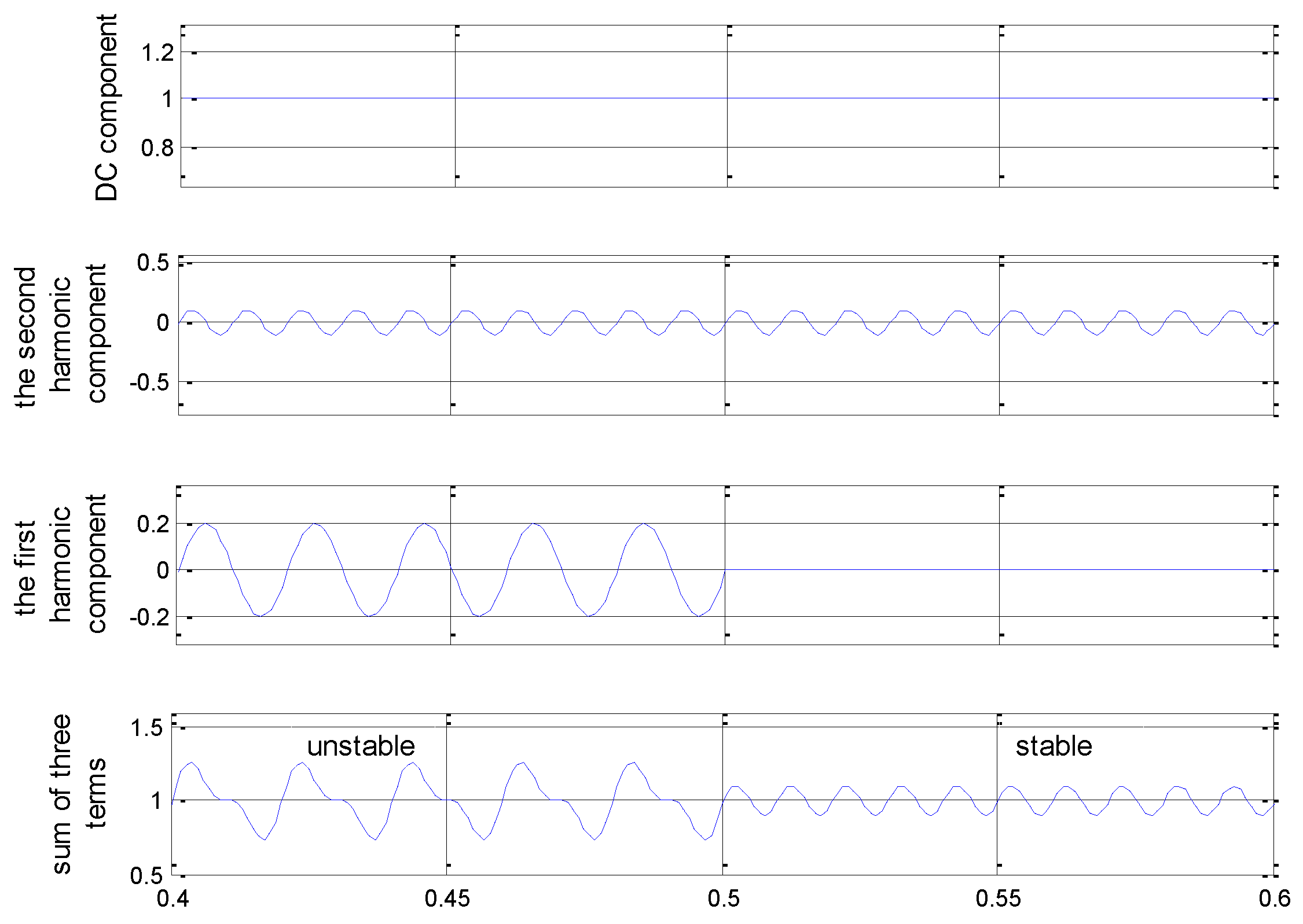
3.1. The First Harmonic Component

We obtain the steady-state solution by making all time-derivatives in Equations (16)–(21) equal to zero. Therefore, Equation (17) becomes:
( j ω m C 2 + 1 R ) ( x 0 x 1 r + x 1 r x 2 r + x 1 i x 2 i + j ( x 0 x 1 i + x 1 r x 2 i x 1 i x 2 r ) ) = V m 2 R s ( 1 + β ) V r e f ( y 1 r 4 + j 3 y 1 i 4 ) .
Considering the real and imaginary part of Equation (22), one has:
{ 1 R ( x 0 x 1 r + x 1 r x 2 r + x 1 i x 2 i ) ω m C 2 ( x 0 x 1 i + x 1 r x 2 i x 1 i x 2 r ) = V m 2 R s ( 1 + β ) V r e f y 1 r 4 ω m C 2 ( x 0 x 1 r + x 1 r x 2 r + x 1 i x 2 i ) + 1 R ( x 0 x 1 i + x 1 r x 2 i x 1 i x 2 r ) = V m 2 R s ( 1 + β ) V r e f 3 y 1 i 4 .
Equation (23) has another form, which is the following:
( x 1 r x 1 i ) = V m 2 4 R s ( 1 + β ) V r e f ( 1 R 2 + ω m 2 C 2 4 ) ( x 0 2 ( x 2 r 2 + x 2 i 2 ) ) × ( x 0 x 2 r R + ω m C x 2 i 2 3 ( x 2 i R ω m C ( x 0 x 2 r ) 2 ) x 2 i R ω m C ( x 0 + x 2 r ) 2 3 ( x 0 + x 2 r R ω m C x 2 i 2 ) ) ( y 1 r y 1 i ) .
By making all time derivatives in Equation (20) equal to zero, one has:
C z j ω m ( y 1 r + j y 1 i ) = g m 1 1 + β ( x 1 r + j x 1 i ) g m R g m C z 1 1 + β j ω m ( x 1 r + j x 1 i ) .
Considering the real and imaginary part of Equation (25), one obtains:
{ C z ω m y 1 i = g m 1 1 + β x 1 r + g m R g m C z 1 1 + β ω m x 1 i C z ω m y 1 r = g m 1 1 + β x 1 i g m R g m C z 1 1 + β ω m x 1 r .
Equation (26) can be written as:
( y 1 r y 1 i ) = 1 C z ω m ( g m R g m C z 1 1 + β ω m g m 1 1 + β g m 1 1 + β g m R g m C z 1 1 + β ω m ) ( x 1 r x 1 i ) .
Equations (24) and (27) describe the transfer function of the first harmonic component in the main circuit and the control circuit of the converter, respectively. By integrating them, one has the total transfer function as follows:
M = 1 C z ω m ( g m R g m C z 1 1 + β ω m g m 1 1 + β g m 1 1 + β g m R g m C z 1 1 + β ω m ) × V m 2 4 R s ( 1 + β ) V r e f ( 1 R 2 + ω m 2 C 2 4 ) ( x 0 2 ( x 2 r 2 + x 2 i 2 ) ) × ( x 0 x 2 r R + ω m C x 2 i 2 3 ( x 2 i R ω m C ( x 0 x 2 r ) 2 ) x 2 i R ω m C ( x 0 + x 2 r ) 2 3 ( x 0 + x 2 r R ω m C x 2 i 2 ) ) .
One needs the DC component and the second harmonic component before studying Equation (28).

3.2. The DC Component and the Second Harmonic Component

The DC component and the second harmonic component are computed from Equations (16) and (18). It is important to note that the first harmonic component is smaller than the DC component and the second harmonic component in Equations (16) and (18). Therefore, one has:
C 2 d d t ( x 0 2 + 2 x 2 r 2 + 2 x 2 i 2 ) + 1 R ( x 0 2 + 2 x 2 r 2 + 2 x 2 i 2 ) = V m 2 R s ( 1 + β ) V r e f ( y 0 y 2 r ) .
C 2 d d t ( 2 x 0 x 2 ) + ( j ω m C + 1 R ) ( 2 x 0 x 2 ) = V m 2 R s ( 1 + β ) V r e f ( y 2 1 2 y 0 ) .
Equations (19), (21), (29) and (30) form the model describing the DC component and the second harmonic component. By making all time-derivatives in those four equations equal to zero, one obtains:
1 R ( x 0 2 + 2 x 2 r 2 + 2 x 2 i 2 ) = V m 2 R s ( 1 + β ) V r e f ( y 0 y 2 r ) .
( j ω m C + 1 R ) ( 2 x 0 x 2 ) = V m 2 R s ( 1 + β ) V r e f ( y 2 1 2 y 0 ) .
g m ( V r e f 1 1 + β x 0 ) = 0 .
j 2 C z ω m y 2 = g m 1 1 + β x 2 j 2 ω m g m R g m C z 1 1 + β x 2 .
From Equations (31)–(34), one obtains the DC component and the second harmonic component. The steady-state value of the DC component is:
x 0 = ( 1 + β ) V r e f .
When Equation (35) is satisfied, the second harmonic component is zero. Now we can study Equation (28).

3.3. Stability of the OCC Boost PFC Converter

Based on the DC component and the second harmonic component computed in Section 3.2, one can simplify Equation (28) into:
M = g m C z ω m V m 2 4 R s ( 1 + β ) 2 V r e f ( 1 R 2 + ω m 2 C 2 4 ) x 0 ( R g m C z ω m R + ω m C 2 3 R g m C z ω m 2 C 2 3 R 1 R + R g m C z ω m 2 C 2 3 ω m C 2 3 R g m C z ω m R ) .
It is important to note that M in (36) is the round-trip signal transfer function of the first harmonic component. When all eigenvalues of M are less than 1, the first harmonic component converges to zero. At the same time, the DC component and the second harmonic component are almost constant, as shown in Section 3.2 and Figure 2. Therefore the converter operates in a stable manner. When the absolute values of one eigenvalue of M is more than 1, the first harmonic component does not converge to zero. The converter begins to exhibit period-doubling bifurcation at the line frequency [24]. Therefore, the criterion of the stability of the converter is the eigenvalues of matrix M.

4. Non-Linear Phenomena of the OCC Boost PFC Converter

To verify the above-mentioned theory, simulations and experiments are conducted. The same circuit topology is adopted (Figure 1). The parameters in the converter are shown in Table 1, unless otherwise specified.
In the converter, the input voltage and the output capacitance are two important parameters, which are selected in the design process. In this paper, the effect of these parameters on the non-linear phenomena of the converter is studied. Figure 3 shows the stability boundaries obtained from theoretical calculation based on Equation (36) and simulation experiment. From Figure 3, we have the following conclusions.
  • The effect of the input voltage on the stability of the converter. Figure 3 shows that when the capacitance is fixed and the input voltage increases, the converter may lose stability.
  • The effect of the output capacitance on the stability of the converter. Figure 3 shows that when the input voltage is increased, a larger output capacitance is needed in order to assure stable operation of the converter. This result is important because a larger output capacitance affects the dynamic performance of the converter.
  • The difference between the two boundaries lies in the fact that some approximations are taken in the analysis, and only the first and the second harmonic components are taken into consideration.
The simulation waveforms of the output voltage and the inductor current are shown in Figure 4 and Figure 5 when the input voltage V m = 40   V and V m = 66.5   V , respectively. (For the MATLAB model file, please contact the corresponding author by e-mail: [email protected].) In Figure 4, the converter operate stably. In Figure 5, the converter exhibits line frequency instability as a result of the period-doubling bifurcation at the line frequency. The instability reduces the power factor of the converter to be considerably lower than 1. If the input voltage increases further, the converter may exhibit chaotic phenomena.

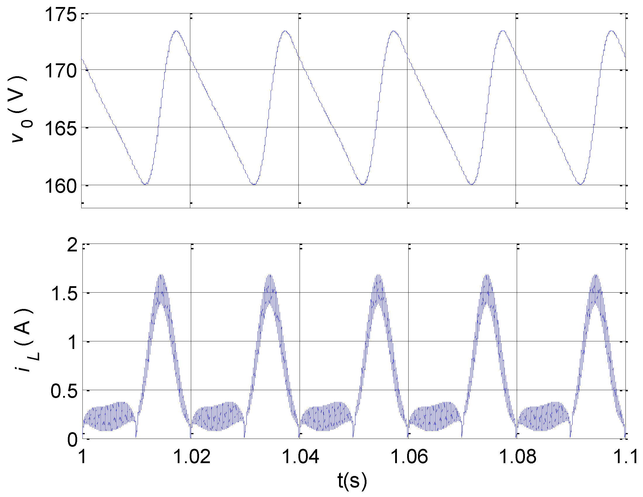
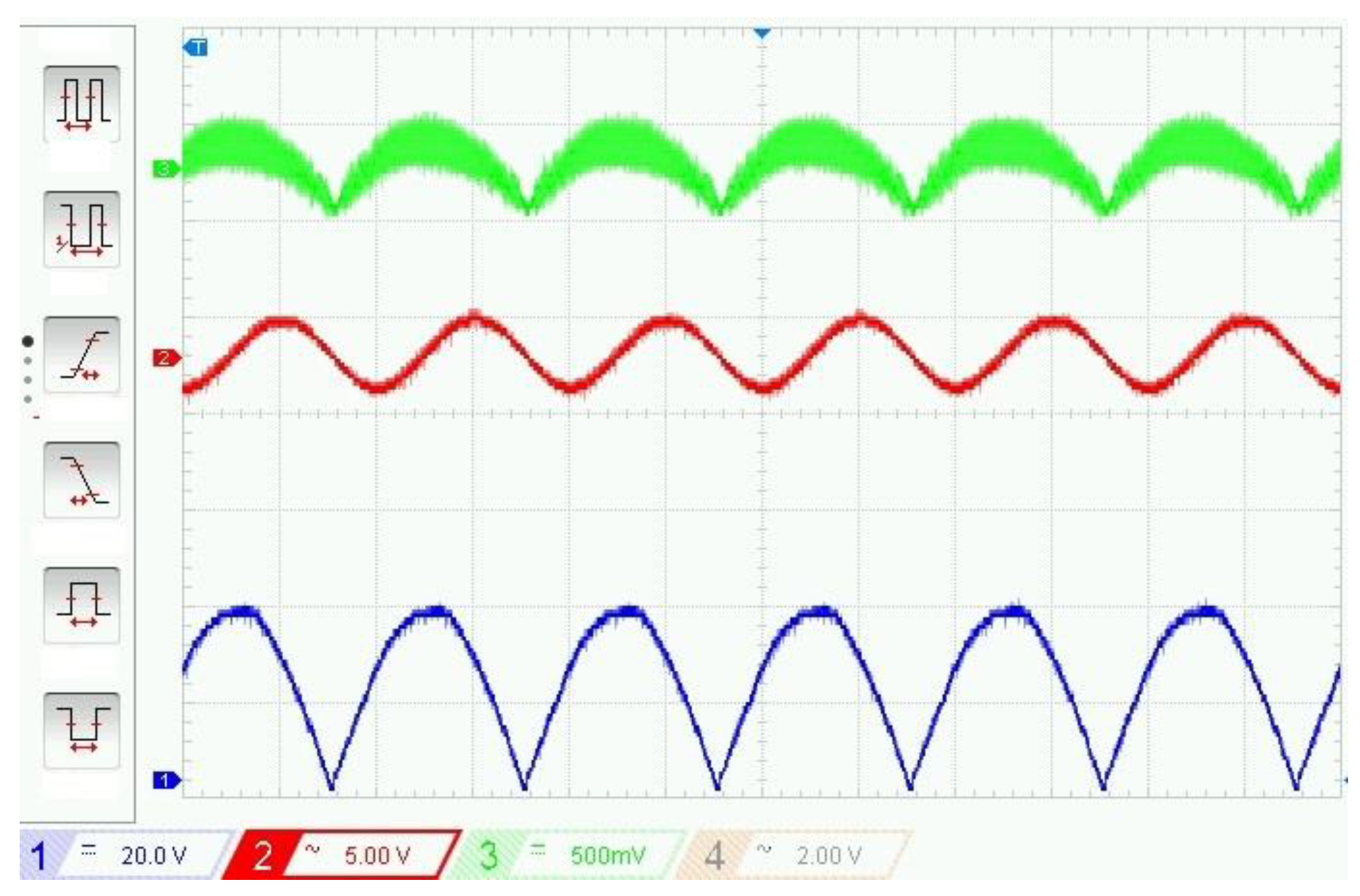
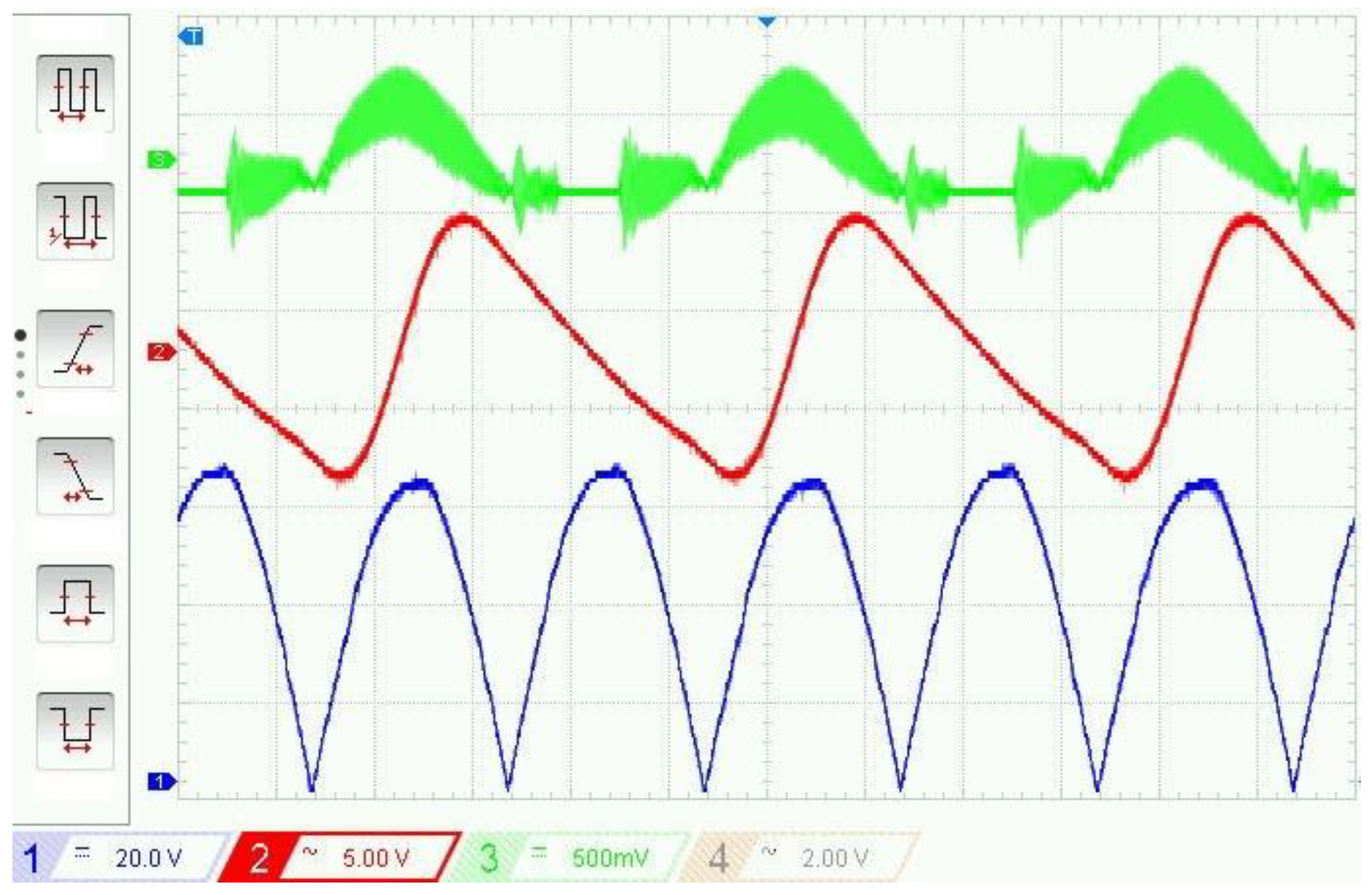
5. Experimental Verifications

To verify the line frequency instability from the theoretical analysis, an experimental circuit prototype was implemented using IR1150 (Infineon Technologies AG, Neubiberg, Germany), which is a classical OCC Boost PFC IC. In our experiment, the circuit parameters are identical to the above theoretical analysis. The current probe (FLUKE i5s, Everett, WA, USA) AC (400 mV/A) current clamp is used to detect the line current. The input voltage, the inductor current and the output voltage (AC coupling) are shown in Figure 6 and Figure 7 when the input voltage V m = 40   V and V m = 68   V , respectively. In Figure 6, the converter operates in a stable manner and the frequencies of all waveforms are 100 Hz. In Figure 7, the converter exhibits period-doubling phenomena. Furthermore, the first harmonic frequency of the inductor current and the output voltage ripple are 50 Hz, which is half of the rectified AC voltage. As shown in Figure 6 and Figure 7, the experimental results are consistent with the analytical results. It is important to note that when the PFC converter exhibits period-doubling bifurcation, the voltage ripple of the output voltage is larger compared with the normal operation. This value is important for the performance and lifetime of a electrolytic capacitor.

6. Conclusions

The OCC PFC converters have a simpler control circuit compared to the traditional averaged current mode PFC converters. In this paper, the method of double averaging was adopted to study the dynamics of an OCC Boost PFC converter. The first averaging is applied to the switching period, and the second averaging is applied to the line period. We derived the round-trip signal transfer function of the first harmonic component in the converter, and the stability of the converter is decided by the eigenvalues of the round-trip signal transfer function. By calculating the eigenvalues, we gave theoretical prediction of the stability of the converter under different output capacitors. Simulation and experimental results verified theoretical prediction. The method of double averaging can predict nonlinear phenomena which traditional method cannot predict. It is important to note that when the OCC PFC converter exhibits line frequency instabilities, the power factor decreases dramatically. Therefore, theoretical analysis in this paper is of great importance in designing the OCC PFC converter.

Author Contributions

R.Z. and W.M. designed the experiment, drafted the manuscript; L.W. and M.H. conducted the experiment; L.C., H.Z. and Y.Z. reviewed and refined the paper.

Acknowledgments

This research is supported by the National Natural Science Foundation of China under Grant 51377188.

Conflicts of Interest

The authors declare no conflicts of interest with respect to the research, authorship, and/or publication of this article.

Appendix A

Some important properties:
( d u ( t ) d t ) k = d u k ( t ) d t + j k ω m u k .
( u ( t ) cos 2 ω m t ) k = 1 2 ( u k 2 + u k + 2 ) .
( u 2 ( t ) ) 0 = u 0 2 + 2 | u 1 | 2 + 2 | u 2 | 2 .
( u 2 ( t ) ) 1 = 2 u 0 u 1 + 2 ( u 1 r u 2 r + u 1 i u 2 i + j ( u 1 r u 2 i u 1 i u 2 r ) ) .
( u 2 ( t ) ) 2 = ( u 1 ) 2 + 2 u 0 u 2 .
where u 1 = u 1 r + j u 1 i , u 2 = u 2 r + j u 2 i .

References

  1. García, O.; Cobos, J.A.; Prieto, R.; Alou, P.; Uceda, J. Single phase power factor correction: A survey. IEEE Trans. Power Electron. 2003, 18, 749–755. [Google Scholar] [CrossRef]
  2. Giaouris, D.S.; Banerjee, B.; Zahawi, V. Pickert, Control of fast scale bifurcations in power-factor correction converters. IEEE Trans. Circuits Syst. II 2007, 54, 805–809. [Google Scholar] [CrossRef]
  3. Lai, Z.; Smedley, K.M. A family of continuous-conduction-mode power-factor-correction controllers based on the general pulse-width modulator. IEEE Trans. Power Electr. 1998, 13, 501–510. [Google Scholar]
  4. Orabi, M.; Nimoniya, T. Non-linear dynamic of power factor correction converter. IEEE Trans. Ind. Electron. 2003, 50, 1116. [Google Scholar] [CrossRef]
  5. Iu, H.H.C.; Zhou, Y.F.; Tse, C.K. Fast-scale instability in a PFC boost converter under average current-mode control. Int. J. Circ. Theor. App. 2003, 31, 611–624. [Google Scholar] [CrossRef]
  6. Orabi, M.; Ninomiya, T. Stability investigation of the cascade twostage PFC converter. IEICE Trans. Commun. 2004, E87-B, 3506–3514. [Google Scholar]
  7. Chu, G.; Tse, C.K.; Wong, S.C. Line-frequency instability of PFC power supplies. IEEE Trans. Power Electron. 2009, 24, 469–482. [Google Scholar] [CrossRef]
  8. El Aroudi, A.; Orabi, M.; Haroun, R.; Martínez-Salamero, L. Asymptotic slow-scale stability boundary of PFC AC-DC power converters: Theoretical prediction and experimental validation. IEEE Trans. Ind. Electron. 2011, 58, 3448–3460. [Google Scholar] [CrossRef]
  9. Wang, F.; Zhang, H.; Ma, X. Analysis of slow-scale instability in boost PFC converter using the method of harmonic balance and floquet theory. IEEE Trans. Circuits Syst. Regul. Pap. 2010, 57, 405–414. [Google Scholar] [CrossRef]
  10. El Aroudi, A.; Orabi, M. Stabilizing technique for AC-DC boost PFC converter based on time delay feedback. IEEE Trans. Circuits Syst. Express Briefs 2010, 57, 56–60. [Google Scholar] [CrossRef]
  11. Ma, W.; Wang, M.; Liu, S.; Li, S.; Yu, P. Stabilizing the average current-mode-controlled boost PFC converter via washout-filter-aided method. IEEE Trans. Circuits Syst. Express Briefs 2011, 58, 595–599. [Google Scholar] [CrossRef]
  12. Zou, J.; Ma, X.; Tse, C.K.; Dai, D. Fast-scale bifurcation in power-factor-correction buck-boost converters and effects of incompatible periodicities. Int. J. Circuit Theory Appl. 2006, 34, 251–264. [Google Scholar] [CrossRef]
  13. Wu, X.; Tse, C.K.; Dranga, O.; Lu, J. Fast-scale instability of single-stage power-factor-correction power supplies. IEEE Trans. Circuits Syst. Regul. Pap. 2006, 53, 204–213. [Google Scholar] [Green Version]
  14. Wong, S.-C.; Tse, C.K.; Orabi, M.; Ninomiya, T. The Method of Double Averaging: An Approach for Modeling Power-Factor-Correction Switching Converters. IEEE Trans. Circuits Syst. Regul. Pap. 2006, 53, 454–464. [Google Scholar] [CrossRef]
  15. Orabi, M.; Haron, R.; Youssef, M.Z. Stability analysis of PFC converters with one-cycle control. In Proceedings of the 31st International Telecommunications Energy Conference, Incheon, Korea, 18–22 October 2009. [Google Scholar]
  16. Smedley, K.M.; Cuk, S. One-Cycle Control of Switching Converters. IEEE Trans. Power Electr. 1995, 10, 625–633. [Google Scholar] [CrossRef]
  17. Smedley, K.M.; Cuk, S. Dynamics of One-Cycle controlled cuk converters. IEEE Trans. Power Electr. 1995, 10, 634–639. [Google Scholar] [CrossRef]
  18. Fang, C.C.; Abed, E.H. Robust feedback stabilization of limit cycles in PWM DC-DC converters. Nonlinear Dyn. 2002, 27, 295–309. [Google Scholar] [CrossRef]
  19. Fang, C.-C. Sampled-Data modeling and analysis of One-Cycle control and charge control. IEEE Trans. Power Electr. 2001, 16, 345–350. [Google Scholar] [CrossRef]
  20. Lee, F.; Iwens, R.; Yu, Y.; Triner, J. Generalized computer-aided discrete time domain modeling and analysis of dc-dc converters. In Proceedings of the 1977 IEEE Power Electronics Specialists Conference, Palo Alto, CA, USA, 14–16 June 1977. [Google Scholar]
  21. Sanders, S.R.; Verghese, G.C. Synthesis of averaged circuit models for switched power converters. IEEE Trans. Circuits Syst. 1991, 8, 905–915. [Google Scholar] [CrossRef]
  22. Maksimovic, D.; Zane, R.; Erickson, R. Impact of digital control in power electronics. In Proceedings of the 16th International Symposium on Power Semiconductor Devices & ICs, Kitakyushu, Japan, 24–27 May 2004. [Google Scholar]
  23. Caliskan, V.A.; Verghese, O.C.; Stankovic, A.M. Multifrequency averaging of DC/DC converters. IEEE Trans. Power Electron. 1999, 1, 124–133. [Google Scholar] [CrossRef]
  24. Dorf, R.C.; Bishop, R.H. Modern Control Systems, 11th ed.; Pearson Education, Inc.: Upper Saddle River, NJ, USA, 2008. [Google Scholar]
Figure 1. Circuit diagram of the OCC Boost PFC converter and its operating principle.
Electronics 07 00203 g001
Figure 2. Illustration of stable and unstable operation of the converter.
Electronics 07 00203 g002
Figure 3. Stability boundaries of the input voltage obtained from the theoretical calculation and simulation experiment.
Electronics 07 00203 g003
Figure 4. Simulation waveforms of the output voltage and the inductor current when the input voltage V m = 40   V , the load R = 1600   Ω and the output capacitance C = 100   μ F .
Electronics 07 00203 g004
Figure 5. Simulation waveforms of the output voltage and the inductor current when the input voltage V m = 66.5   V , the load R = 1600   Ω and the output capacitance C = 100   μ F .
Electronics 07 00203 g005
Figure 6. Experimental waveforms of the converter when the input voltage V m = 40   V , the load R = 1600   Ω and the output capacitance C = 100   μ F . CH1: the input voltage (20 V/div), CH3: the inductor current (500 mV/div) and CH2: the output voltage (5 V/div) (AC coupling).
Electronics 07 00203 g006
Figure 7. Experimental waveforms of the converter when the input voltage V m = 68   V , the load R = 1600   Ω and the output capacitance C = 100   μ F . CH1: the input voltage (20 V/div), CH3: the inductor current (500 mV/div) and CH2: the output voltage (5 V/div) (AC coupling).
Electronics 07 00203 g007
Table 1. Parameters in the OCC Boost PFC converter.
SymbolQuantityUnit
Ts15 μ s
ωm100πrad/s
L2mH
C100 μ F
Rf1849kΩ
Rf237.3kΩ
Rgm10.25kΩ
Cz32nF
Cp32pF
Vref7V
Rs0.645Ω
R(load)1600Ω
gm40 μ S

