Article

Wireless Power Transfer for Battery Powering System

1
School of Electronic Information and Electrical Engineering, Shanghai Jiao Tong University, Shanghai 200240, China
2
College of Electric and Information Engineering, Zhengzhou University of Light Industry, Zhengzhou 450002, China
*
Author to whom correspondence should be addressed.
Electronics 2018, 7(9), 178; https://doi.org/10.3390/electronics7090178
Submission received: 18 August 2018 / Revised: 30 August 2018 / Accepted: 5 September 2018 / Published: 7 September 2018
(This article belongs to the Special Issue Applications of Power Electronics)

Abstract

:
The LCL topology (formed by an LC tank with a transmitting coil) is extensively utilized in wireless power transfer (WPT) systems with the features of a constant resonant current and ability to disconnect load abruptly. However, it requires high input voltage, which limits its utilization in battery powering scenarios (12~24 V). A current-fed inverter (CFI) is applied to the LCL-S (a compensation capacitor in series with the receiving coil) WPT systems to boost the input voltage, thereby getting a higher resonant current in the transmitting side (Tx). To facilitate the voltage regulation in the receiving side (Rx), a semi-active bridge (SAB) is introduced into the system, which further boosts the output voltage by a lower frequency switching at different duty ratios. Rigorous mathematical analysis of the proposed system is carried out and design guidelines are subsequently derived. Moreover, a power loss reduction is realized by zero voltage switch (ZVS) of the four switches in the Tx which are deduced and presented. Simulations and experiments are added to verify the proposed system. Consequently, a 93.3% system efficiency (DC-to-DC efficiency) is obtained using the proposed topology. Optimization techniques for a higher efficiency are included in this study.

1. Introduction

Nowadays, wireless power transfer (WPT) technology is a leading research field due to the wide spread electronic devices that can benefit from this technology. For instance, electric vehicles can get rid of electrical hazards caused by wire snapping and reduce on-board battery burden by dynamic charging [1,2,3]. Medical implants benefit from the increased power supply without the penalty of a greater bulk [4,5]. In addition, a WPT charger can power multiple loads simultaneously without lots of wires and complex connections. Accordingly, it can be predicted that WPT will be a good assistant of, or an alternative to the plug-in power transfer in various voltage rate systems. The advantages and prospects have already ignited a hot interest all over the world, and related studies are burgeoning.
In WPT systems, the compensation topologies are very crucial for high efficiency and power rates by reducing and even cancelling leakage inductance. Research on compensation topologies and their features are continually carried out and new ideas have been investigated and put forward as well [6,7,8,9]. Many research works rely on four basic topologies, namely series-series (SS), series-parallel (SP), parallel-parallel (PP), and parallel-series (PS) [10]. However, to meet special or practical requirements, such as constant current/voltage output [7,11] and the endurance of load tripping, hybrid compensation approaches like LC and LCC [12,13] have been put forward. Although, the hybrid topologies introduce more passive components into the system and may add power loss and system bulk, their benefits overweight the shortcoming for demand and security reasons. Among these topologies, the LCL topology, formed by an LC tank with a transmitting coil, is regarded as an ideal network used in the transmitting side (Tx), due to its ability to maintain the transmitting current constant and independent of the reflected impedance of the receivers [11,14]. Thus, the induced voltage in every receiving side (Rx) is steady. Moreover, if the disconnection happens in the four basic topologies, urgent protection would be needed, or the circuit is over-current burned. The LCL topology can endure unexpected load disconnection, so it is rather promising in practice. Accordingly, the LCL topology is applied in the Tx in this literature due to these features.
Nevertheless, this topology requires a large input voltage or small receiving coil inductance to augment the transmitting current and induce a high voltage in the Rx. Decreasing the coil inductance will lead to a small mutual inductance and a voltage decreasing in the Rx. Hence, enlarging the input voltage is recommended. The input voltage is 400 V in Ref. [9], and the input voltage of the Evatran products is 220 V. Otherwise, the output voltage can be small, only 5 V in Ref. [11] due to the small input of 26 V. For some power sources, such as photovoltaic panels and batteries, the voltage rating of each cell is very low. The output voltage of a solar cell module is around 12~24 V, and the nominal voltage of a lead-acid battery with six cells is only 12 V. Simply increasing the number of panels and cells in series can surge the system bulk, pressure and insulation requirement, thereby being impractical for solar system applications, wearable devices, and other portable equipment. In addition, the WPT technology may be adopted as an aid for safety and reliability in some internal sub-systems, where only low-voltage sources can be provided.
To extend the WPT technology and LCL topology to battery powering system and wirelessly power the loads within the 12~24 V input range, front-end boost circuits are in great need. Inserting the traditional boost circuits before the inverter is a good solution and also generally used. High efficiency of the boost circuits can be obtained due to the maturity of boost techniques. However, lots of components (an active switch, a power diode, a comparably large inductor, and a capacitor) and auxiliary circuits (control circuits and drivers) are needed. In contrast, the Z-source/quasi-Z-source networks boost the output voltage by shorting the end-rear bridge, which can be realized by the full bridge inverter itself and the extra control circuits are not required [15]. Nevertheless, two inductors and two capacitors are added so the losses caused by these components increase inevitably and the system may incur maloperations caused by the resonant networks [16,17,18]. On the other hand, large inductances are required in the Z-source network to suppress the ripples and prevent the discontinuous current mode [19]. Hence these two mentioned circuits will increase the bulk of the power system, which may cause difficulty in carrying or assembling.
To realize a high conversion gain and a compact size with a simpler topology, a current-fed inverter (CFI) is a good alternative in WPT systems. The CFI only contains a full bridge inverter and two identical front-end inductors so that the power conversion stages are reduced with an improvement in reliability [20,21]. Compared with the voltage source inverter (VSI) in series with a boost circuit, the CFI has a simpler circuit and easier control method. The control and response rates are also improved due to the compact stages. Compared with the Z-source inverter (ZSI), the CFI has less components and reduces the total harmonic distortion (THD) of the input current. Moreover, the switches in the CFI can operate ZVS from inductive impedance to capacitive impedance and the top-side switches can be turned OFF softly in some scenarios.
Conventionally, there are two kinds of schemes to regulate the output voltage. One scheme is to apply a diode rectifier in the Rx but conduct the optimal charge control in the Tx (the source voltage level shift, the duty ratio adjustment, etc.). This scheme predigests the Rx complexity but needs frequent and quick communications. Another scheme is to control the Rx by itself, which lowers the communication demand. Two circuits have already been proposed: inserting the buck-boost converter connected in series with the rectifier [22] or replacing the rectifier with an active bridge [23]. The former involves a large inductor and more control circuits. The latterrequires a complicated controller and complex auxiliary circuits with increasing receiving volume, which is not as compact as mobile devices require. Considering the trade-off between the size and communication complexity, an active switch replaces one diode of the rectifier and regulates the load voltage in this literature. This semi-active bridge (SAB) can regulate the output by being operated at a variable frequency and duty ratio. Specially, the SAB can boost the output, which can obtain higher voltage than the diode rectifier. Different from the switches in an active bridge that must operate at a high and precise resonant frequency, the switch in SAB can conduct at a lower frequency. Additionally, the complex control protocols and negotiation required by the active bridge [24] are not necessary for the SAB.
The paper is structured as follows: Section 2 depicts the proposed circuit diagram of the WPT system, followed by its operating principle. The capability of soft switching is also elaborated upon. Section 3 models the proposed system with mathematical analyses of the system parameters. Guidelines are provided on the configurations of the inductors, coils, and loads. In Section 4, simulations are implemented, and results are presented and compared. To further support and verify the theoretical analysis and simulation accuracy, a prototype is developed and experimental results are provided in Section 5. A 93.3% system efficiency (DC-to-DC efficiency) is achieved, and the output voltage is within twice to four times that of the input. Optimization techniques for higher efficiency are included. Finally, Section 6 concludes the paper.

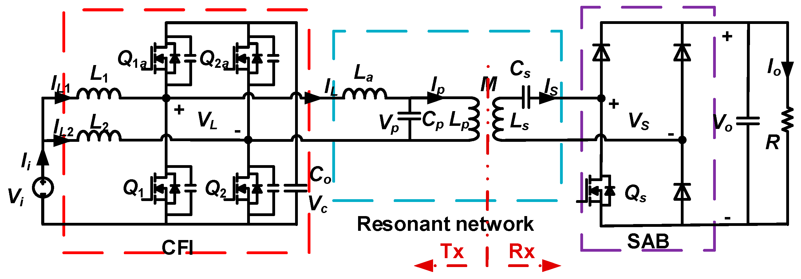
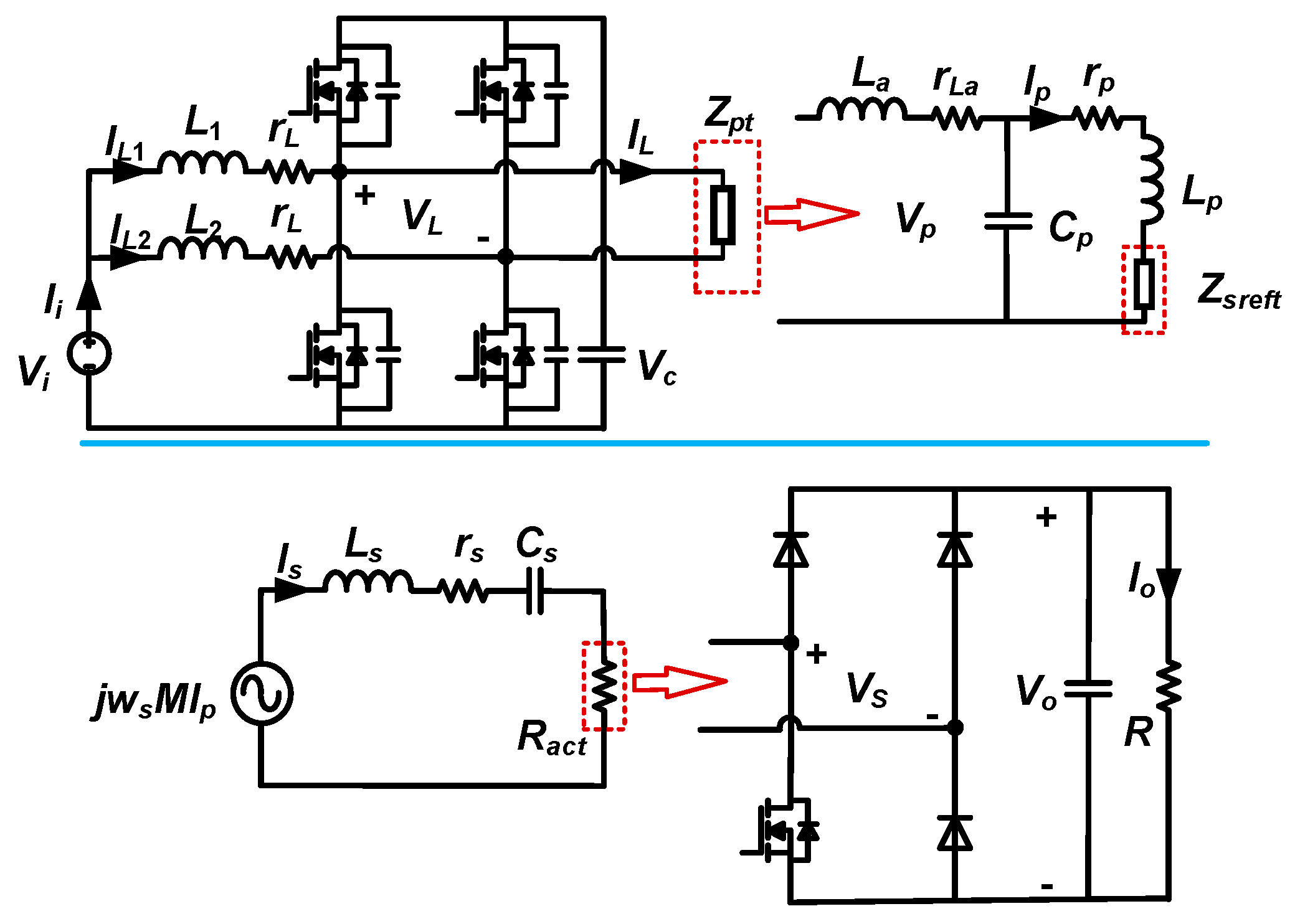
2. Proposed Topology

2.1. System Composition

A block diagram of the proposed topology with one receiver is demonstrated in Figure 1. In the Tx, the CFI contains a clamp capacitor Co, two identical front-end inductors (L1 and L2), and four switches (Q1, Q1a, Q2, and Q2a), which can be regarded as an assembly of two boost converters [20,21]. A combination of the switching pattern and the inductors implement the boost function, and the amplitude of the output voltage is equal to the capacitor voltage VC across Co. For the resonant network, the LCL topology and series compensation topology is employed in the Tx and Rx, respectively. As for the Rx, the SAB supersedes the rectifier, where a bottom side diode is replaced by a controllable switch Qs.
In this paper, bold italic letters symbolize the phasors and the italic letters symbolize the real numbers or RMS values. In Figure 1, Lp and Cp represent the Tx coil inductance and its compensation capacitance. Ls and Cs represent the Rx coil inductance and its compensation capacitance. La and M represent the compensation inductance and mutual inductance. Vi and Ii are the input voltage and input current from the source. VL and IL are the output voltage and current of the CFI. Vp and Ip are the voltage across and the current through Tx coil. Vs and Is are the input voltage of the SAB and the resonant current in the resonant tank.

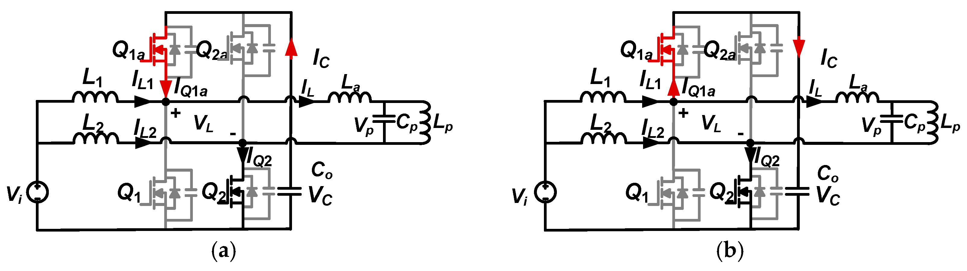
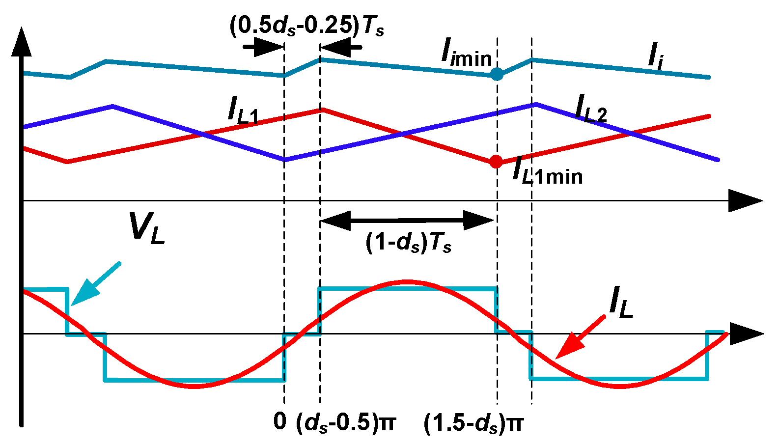
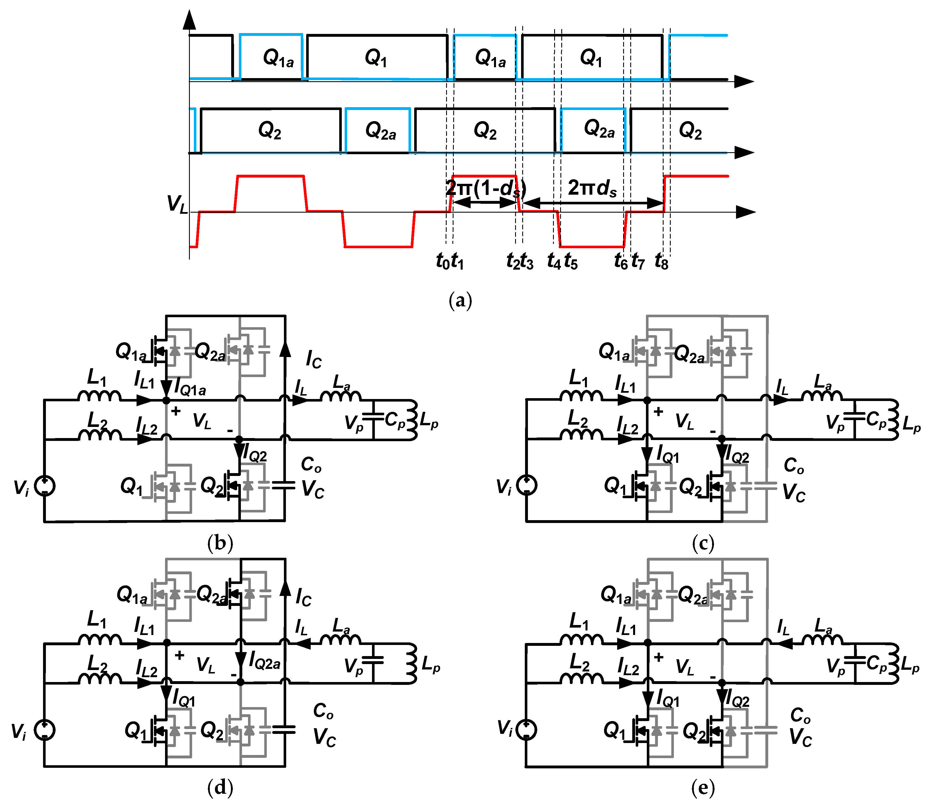
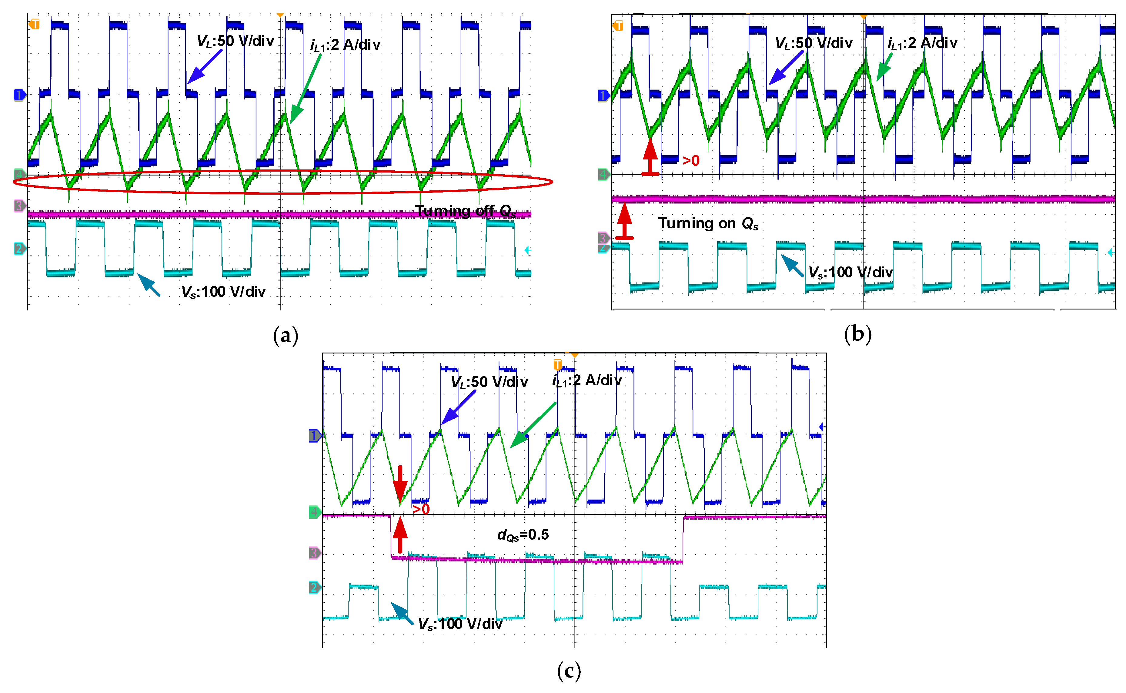
2.2. Operation Patterns in Tx

Theoretically, four states exist in the full bridge. However, if the top-side switches are both ON, the charging circuits for L1 and L2 are broken and the voltage-boost function cannot be accomplished. Thus, three states are conducted in the CFI. Defining the duty ratio of Q1 and Q2 as ds, ds should be above 0.5 to prevent Q1a and Q2a being both ON. The unequal PWM control [25] is adopted in this paper and the corresponding waveforms are depicted in Figure 2a. The four switches all conduct at a resonant frequency fs. When Q1a and Q2 are ON, VL is positive, L1 is discharged but L2 is charged, as shown in Figure 2b. When Q2a and Q1 are ON, VL is negative, L1 is charged but L2 is discharged, as shown in Figure 2d. When the bottom-side switches are ON, VL is zero, both L1 and L2 are charged, as shown in Figure 2c,e.
The current stress of each switches is estimated as
{ I Q 1 a max = I L m I L 1 min I Q 1 max = I L m + I L 1 max I Q 2 a max = I L m I L 2 min I Q 2 max = I L m + I L 2 max .  
As can be seen, the bottom-side switches suffer higher stresses than the top-side switches. According to the boost converter properties [26], the peak-to-peak current ripple and the maximum value of the inductor currents in Discontinuous Conduction Mode (DCM) are larger than those in Continuous Conduction Mode (CCM) under the same load conditions. Due to the rear-end resonant current, L1 and L2 will not enter DCM but quasi-CCM, where the currents through the inductors reverse their direction and the inductors are charged by the resonant network. The current ripple in quasi-CCM is large and the switches will suffer large stresses, according to Equation (1). Consequently, the CFI in this paper is recommended to operate in CCM to decrease the current stresses of the bottom switches. Thus, the two front-end inductors L1 and L2 should be well designed.

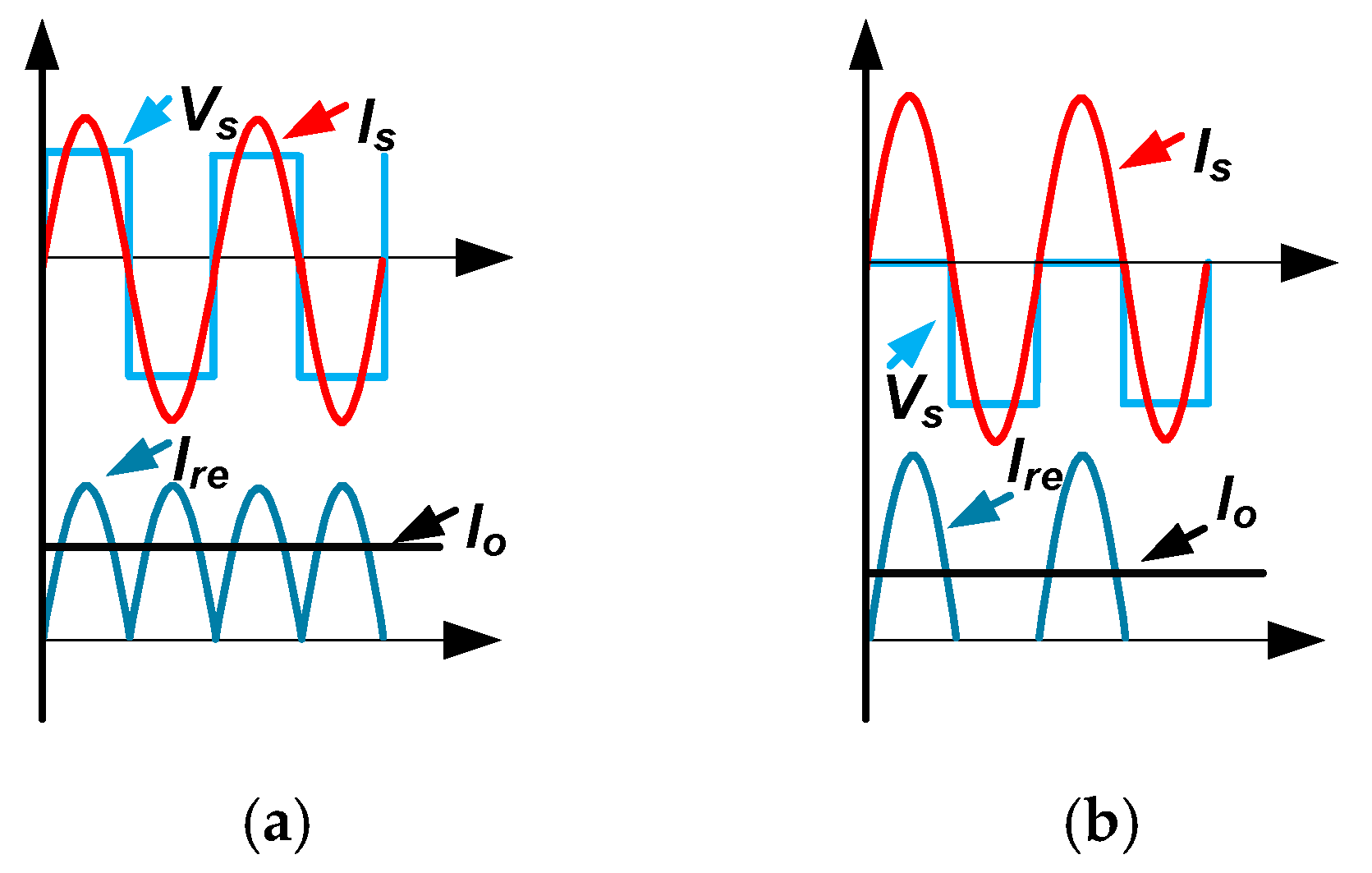
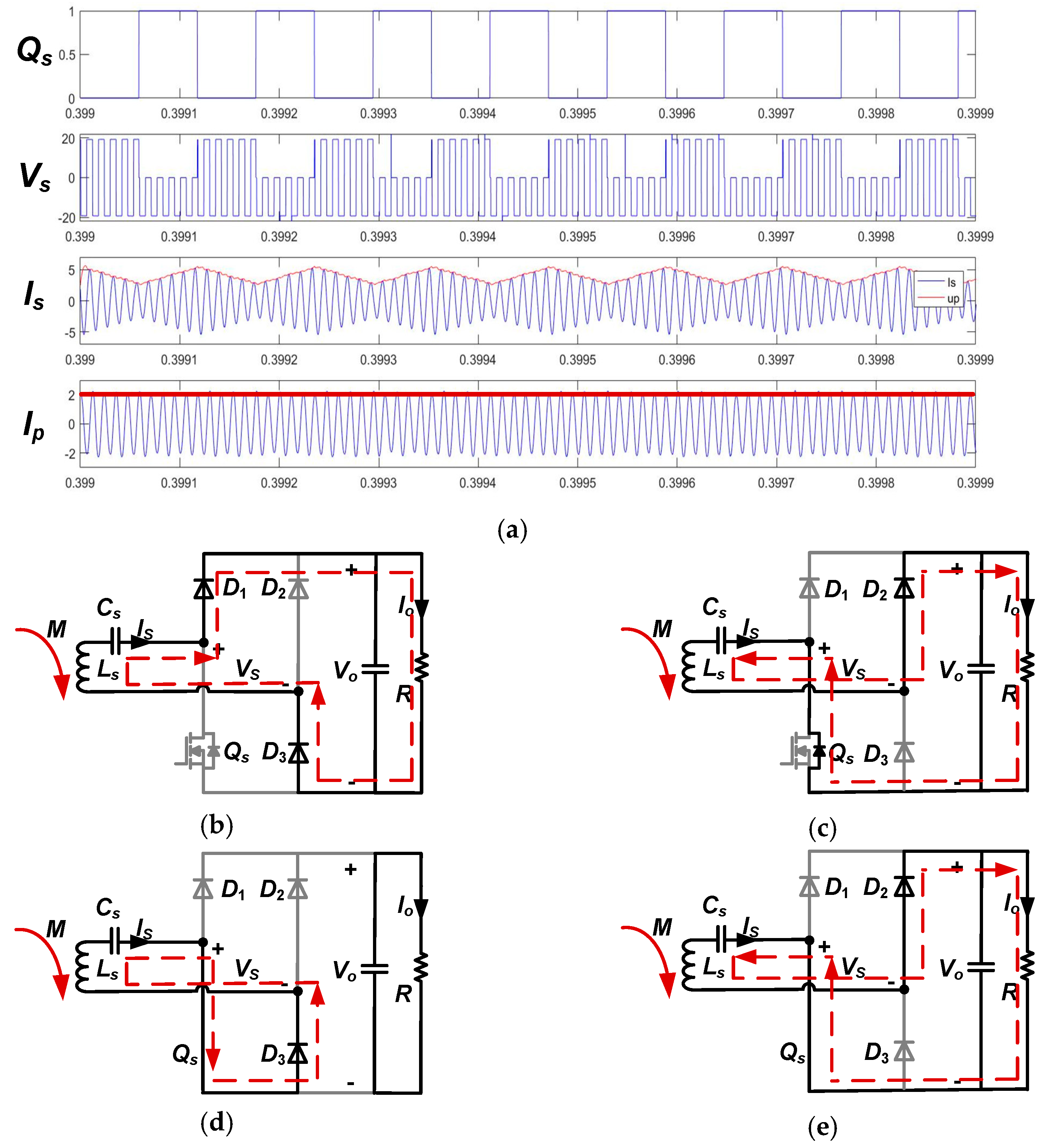
2.3. Operation Patterns in Rx

In the receiving side, Qs operates at frequency fQs. The ratio of fs and fQs is denoted as n (>1), and the duty ratio of Qs is denoted as dQs. Parts of the waveforms and the corresponding patterns are illustrated in Figure 3. The direction of the dark arrow of Is is chosen as a reference direction and the red dotted lines denote the actual current paths. When Qs is turned OFF, it functions as a common diode. The duty ratio of Qs is 0.5 and the corresponding waveforms of Vs, Is, Ip are presented in Figure 3a. Is flows as shown in Figure 3b,c, where Vs is positive and negative, respectively. When Qs is turned ON, the anode of D1 is directly connected with the anode of D3 as shown in Figure 3d,e. When Is is positive, as shown in Figure 3d, it flows straight from one end of the compensation capacitor to the end of the Tx coil, that is, the load R is cut off from the resonant source and Vs drops to zero. When Is is negative, as shown in Figure 3e, however, it flows through D2 and powers the parallel capacitor and the load. At that time, Vs is negative as shown in Figure 3a. Therefore, Is resonates at fs, while the frequency of its envelope line is fQs. On the other hand, the amplitude of Ip can be deemed as a constant value, although the equivalent load changes frequently as mentioned. Hence, the Rx can achieve a stable induced voltage ignoring the rapid change of the equivalent impedance, which is also the reason for choosing the LCL topology as the SAB and LCL complement each other.

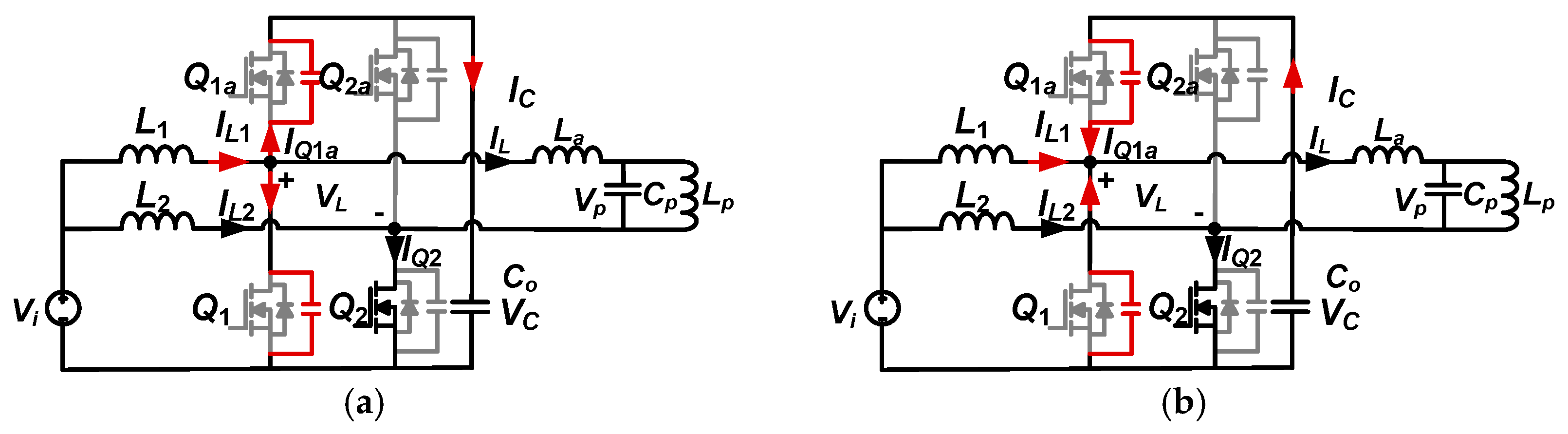
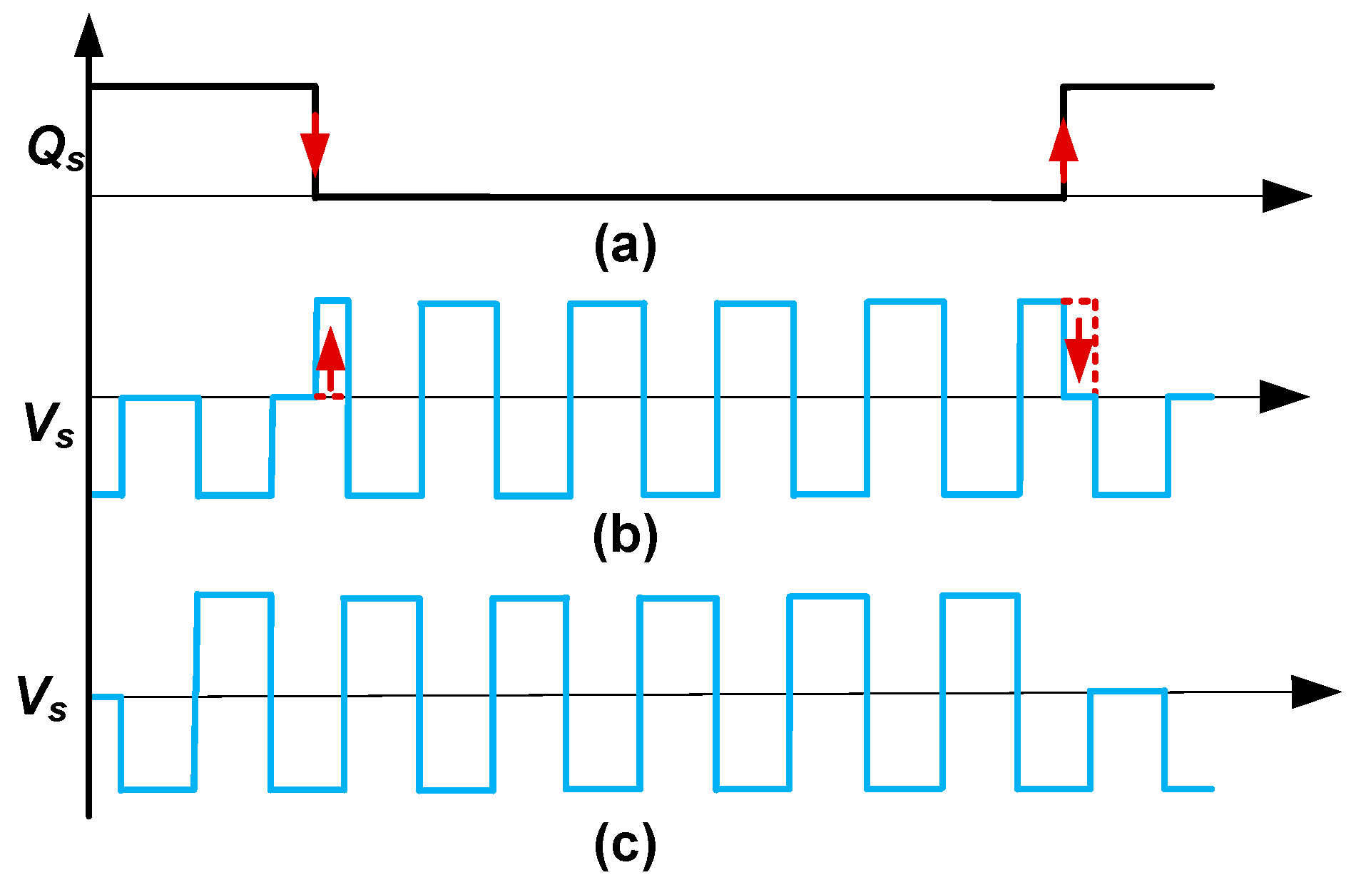
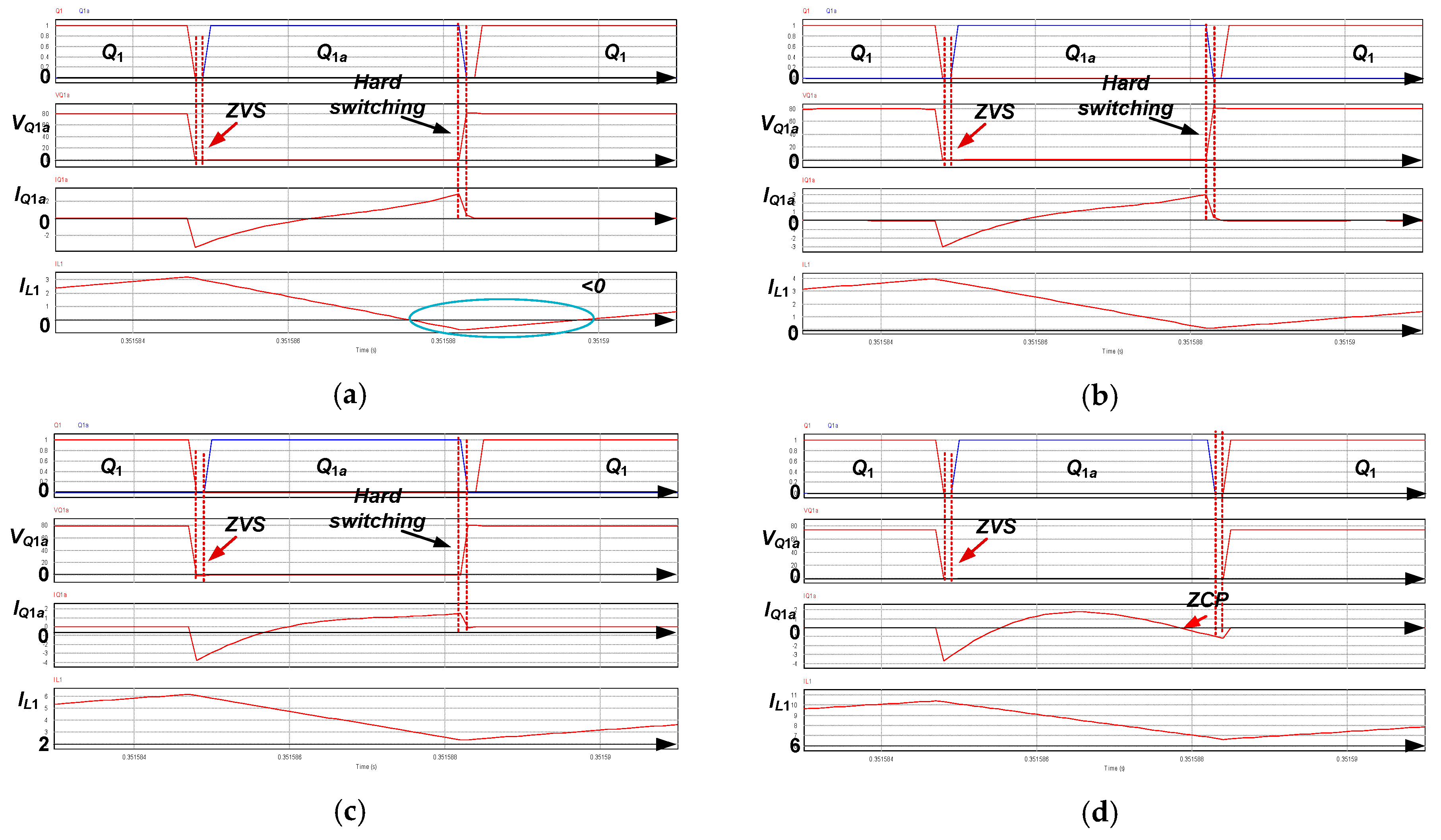
2.4. Soft-Switching Capability

In the Tx, the soft-switching operation is accomplished by the CFI and the clamp capacitor Co. Q1 and Q1a are chosen to illustrate the soft-switching process. The analysis of Q2 and Q2a is fundamentally the same as the analysis of Q1 and Q1a due to the topology symmetry. The current paths are depicted in Figure 4.
Figure 4a shows the state before Q1a is ON, where IL1 reaches its maximum value. The difference between IL1 and IL is positive. The current difference charges the parallel capacitor of Q1a, CQ1a, and discharges the parallel capacitor of Q1, CQ1. Figure 4b shows the state before Q1 is ON, where IL1 reaches its minimum value. At that time, the difference between IL1 and IL is negative. Then, Co also provides current to charge CQ1 and discharge CQ1a. Hence, ZVS of Q1a and Q1 are achieved.
To turn OFF the top-side switches softly [27], IL1 should be a bit larger than IL before Q1a is OFF so that IQ1a will reverse direction from Figure 5a to Figure 5b. Then, when Q1a is turned OFF, the freewheeling current can flow through the parallel diode, providing a condition for the soft-switching OFF [27].
In comparison with the VSI, the inductors in the CFI can provide the current directly for soft switching, thereof getting rid of the rear-end resonant current limitation. Accordingly, the soft switching can be more likely accomplished.
To guarantee the inductors working in CCM and the minimum value of IL1 larger than IL, the inductance should be large, accompanied with the increase of the internal resistance and power loss caused by the inductors. Thus, the inductance should be set at a reasonable value.
In the Rx, the soft-switching operation [27] can also be realized by Qs being turned ON/OFF when the current and the voltage are negative. If Qs is turned OFF when Is is positive and Vs is zero, the current path will suddenly change from Figure 3d to Figure 3b, leading to a surge of Vs and the hard-switching OFF Qs. Additionally, if Qs is turned ON when Is and Vs are positive, the current path will suddenly change from Figure 3b to Figure 3d, leading to a plunge of Vs and the hard-switching ON of Qs. The distortion waveform of Vs is demonstrated in Figure 6b. However, if Qs is turned ON/OFF when Is is negative, the current pattern switches between Figure 3c and Figure 3e. As can be seen, the voltage output in Figure 6c is ideal and the soft-switching operation is also achieved. To prevent this distortion, Qs should be turned ON when Is is negative, which can be achieved alone in the Rx. In contrast, the dual active bridge (DAB) strictly demands the synchronization [28], otherwise, the system becomes unstable and power oscillations occur.

3. Mathematical Modeling and Configuration

3.1. Equivalent Circuit Model

To model and analyze the proposed system, an equivalent circuit is established as shown in Figure 7. Zp, Zsref, and Rac denote the Tx equivalent impedance, the reflected impedance from the Rx and the equivalent ac resistance calculated in a receiving switching period, respectively. Zpt, Zsreft, and Ract denote the three impedances calculated in a resonant period. rp and rs denote the inner resistances of the Tx coil and the Rx coil. Besides, La is designed to be identical to Lp. Considering the power losses, inner resistance of La is represented by rLa. In addition, rL denotes the inner resistance of L1 and L2. The Tx switching frequency and the resonant frequency are both equalized to fs.
Thus, Zpt is resistant and deduced as:
Z p t = j ω s L a + r L a + ( j ω s L p + Z s r e f t + r p ) 1 j ω s C p j ω s L p + Z s r e f t + r p + 1 j ω s C p = ( ω s L p ) 2 Z s r e f t + r p + r L a ( ω s L p ) 2 Z s r e f t + r p ,
where, Zsreft is equal to
Z s r e f t = ( ω s M ) 2 R a c t + r s .  
Based on the boost model, the amplitude of the square wave VL is derived as:
V L m = V C = V i 1 d s .  
Thus, the RMS value of the fundamental harmonic of VL is deduced as:
V L 1 = 2 2 V i sin π d s π ( 1 d s ) .  
Then, the output current of CFI in a resonant period is:
I L = V L 1 Z p t = 2 2 V sin π d s π ( 1 d s ) ( ω s L p ) 2 [ ( ω s M ) 2 R a c t + r s + r p ] .  
Obviously, IL is load-dependent and its RMS value IL will decrease with the augment of Ract. However, the RMS value of branch current Ip is calculated as:
I p = V L 1 ( Z s r e f t + r p ) ( ω s L p ) 2 1 j ω s C p 1 j ω s C p + j ω s L p + Z s r e f t + r p = V L 1 j ω s L p ,
which signifies that Ip is independent of the Rx characteristics but proportional to the input voltage. Accordingly, high input voltage VL is recommended to maintain a large resonant current. According to the mutual inductance theory, the induced voltage Vs in the Rx keeps steady if Ip is constant.
In the Rx, the model can be presented as:
j ω s M I p = [ j ω s L s + r s + 1 j ω s C s + R a c t ] I s = [ r s + R a c t ] I s ,
which implies that the induced voltage and the receiving current are in-phase.

3.2. Equivalent Resistance of SAB

To analyze the impact of duty ratio dQs and receiving switching frequency fQs (=fs/n) on Rac, Ract, and output voltage Vo, the harmonic approximation method and extended describing function are utilized. Assuming that the induced voltage v(t), receiving current isL(t), and compensation capacitor voltage vsC(t) can be approximated by fundamental terms and the former two are in same phase due to the resistive impedance, it has
{ v ( t ) = ω s M I p m sin ω s t i s L ( t ) = i s L s ( t ) sin ω s t v s C ( t ) = v s C c ( t ) cos ω s t ,
where, the envelope terms are slowly time varying at fs/n.
By utilizing the extended describing method, Vs whose waveform is depicted in Figure 3a, can be approximated as
v s ( t ) f s ( n , d Q s , V o ) sin ω s t .  
The extended describing function fs (n, dQs, Vo) can be calculated by Fourier expansions and given as
f s ( n , d Q s , V o ) = d Q s 2 V o + k = 1 [ a k cos k ω s n t + b k sin k ω s n t ] ,
where the coefficients are
{ a k = V o π k [ i = 1 2 n 2 d Q s n ( 1 ) i sin k φ | π ( i 1 ) / n π i / n i = n d Q s n n 1 sin k φ | 2 π i / n π ( 2 i + 1 ) / n ] b k = V o π k [ i = 1 2 n 2 d Q s n ( 1 ) i 1 cos k φ | π ( i 1 ) / n π i / n + i = n d Q s n n 1 cos k φ | 2 π i / n π ( 2 i + 1 ) / n ] .  
However, it is difficult to get an analytical solution on the relationship between fs, dQs, Vo, and Rac, since the switching frequency is below the resonant frequency and the equivalent impedance in each resonant period is different from others, which is totally contrary to the small-signal model condition [29]. Nevertheless, a trend estimation can be conducted by analyzing the extreme cases. Since the SAB disconnects the load OFF and ON, it can be assumed that when the load is OFF, the equivalent impedance Rac decreases. To validate this assumption and estimate the relation between dQs and Rac, two extreme cases (dQs = 0 and dQs = 1) are considered. The corresponding waveforms are presented in Figure 8.
When Qs stays OFF, that is dQs = 0, the SAB works as a diode rectifier. The typical waveforms are depicted in Figure 8a, where Ire represents the output current of the SAB. Thus, the equivalent ac resistance reaches the maximum as given in [30]:
{ R a c t = R a c R a c max = 8 R π 2 .  
However, when Qs stays ON, that is dQs = 1, the anode of D1 is directly connected with the anode of D3, waveforms change to Figure 8b and the ac load accordingly, is
{ R a c t = R a c R a c max = 2 2 R π 2 .  
It can be found that Rac decreases when dQs increases. Besides, on basis of Equation (6), it can be drawn that the input current IL and input power will rise as dQs increases, and the dc output Vo boost as well due to the energy principles. Thus, the voltage boost function is accomplished.
Assuming that the power loss caused by SAB can be ignored, the power fetched from the Tx is equal to the load power, that is,
V o 2 R = I p 2 ( ω s M ) 2 R a c t + r s R a c t R a c t + r s .  
Hence, by substituting Equations (5), (7), (13) and (14) into Equation (15), the range of the output voltage is estimated as:
2 2 π M R L p ( 8 R + π 2 r s ) sin π d s ( 1 d s ) V i V o 2 0.75 π M R L p ( 2 2 R + π 2 r s ) sin π d s ( 1 d s ) V i ,
which shows the dc load can acquire a wide range of output. Besides, the output voltage Vo can be higher than the input voltage Vi with proper configurations.

3.3. Soft-Switching Design in Tx

The power fetched from the CFI PL during a resonant period is deduced, with Equations (5) and (6), as:
P L = 8 V i 2 ( ω s L p ) 2 sin 2 π d s π 2 ( 1 d s ) 2 [ ( ω s M ) 2 R a c t + r s + r p ] 8 V i 2 ( ω s L p ) 2 sin 2 π d s π 2 ( 1 d s ) 2 [ ( ω s M ) 2 R a c max + r s + r p ] = P L min .  
Assuming that the magnitude of power loss caused by the switches, L1, L2, and Co can be ignored as compared to that of PL, PL is therefore equal to the DC input power Pi, which can be presented as:
P i = 1 2 V i [ 2 I i min + V i L ( 2 d s 1 ) T s ] ,
where, L = L1 = L2, Iimin is the minimum value of the DC input current, illustrated in Figure 9, and can be calculated as
I i min = 2 I L 1 min + V i T s 2 L .  
Accordingly, IL1min can be calculated with Equations (17)–(19) as:
I L 1 min = 4 V i sin 2 π d s π 2 ( 1 d s ) 2 Z p t V i T s 2 L d s .  
To prevent the system from quasi-CCM, IL1min should be above zero. To make IL1min > 0, L can be deduced from Equation (20) with Equation (2) as:
L > T s d s 8 sin 2 π d s π 2 ( 1 d s ) 2 ( ω s L p ) 2 ( ω s M ) 2 R a c t + r s + r p .  
On the other hand, to complete the soft-switching OFF Q1a, it demands
I L 1 min > I L | φ = 1.5 π π d s .  
Defining Q as the loaded quality factor of the Tx, Q can be calculated as:
Q = Z s r e f t ω s L p = ω s k 2 L s ( R a c t + r s ) ,
where k denotes the coupling coefficient.
When Q is large, the output current of CFI is sinusoidal as presented in Figure 9. To complete soft-switching OFF Q1a, Equation (22) is written as:
I L 1 min > 2 I L sin ( 3 2 π π d s ) ,
that is, L is deduced from Equation (24) as:
L > T s d s 8 sin π d s π ( 1 d s ) [ sin π d s π ( 1 d s ) + cos π d s ] ( ω s L p ) 2 ( ω s M ) 2 R a c t + r s + r p .  
Since ds is above 0.5, the right of Equation (21) is larger than that of Equation (25) and reaches its maximum when ds is 0.5. Hence, the inductance should meet the requirement as:
L > π 2 64 f s ( ω s L p ) 2 ( ω s M ) 2 R a c t + r s + r p .  
Nevertheless, considering the inner resistances and power losses of the two inductors at high input current, L cannot increase blindly otherwise the system efficiency will degrade.
However, when Q is small (i.e., Q < 1 according to the MATLAB and PLECS simulation), IL distorts and IQ1a can never reverse direction no matter how large L is, thereby failing soft-switching OFF Q1a and Q2a. In practice, the inner resistances of the coils will surge significantly with the increase of the coil inductance. On the other hand, the LCL topology requires rigorous manufacturing technique to reduce the coil resistance since the losses of the coil resistors in LCL topology far outweigh that in series compensation topology. Accordingly, Lp and M are usually small, which inevitably results in a small Q and distortion of IL. Simply increasing Ls can reduce the receiving efficiency due to the enlarged coil resistance, leading to the system efficiency decreasing as well. Thus, there is a trade-off between the soft-switching OFF and system efficiency.

3.4. Optimal Load

To evaluate the system efficiency variation caused by the change of the equivalent impedance, the optimal load is calculated. Given that the power loss caused by the CFI is hard to theoretically calculated, the transmitting efficiency η, defined as the ratio of the CFI output power to the equivalent ac power, is presented to calculate the optimal load for the CFI and approximate the system efficiency. η can be written with Equations (3), (5)–(7) as:
η = I p 2 Z s r e f t V L 1 I L = ( ω s M ) 2 R a c t r p R a c t 2 + ( ω s M ) 2 R a c t + 2 r s r p R a c t + ( ω s M ) 2 r s + r s 2 r p .  
The derivative of Equation (27) is calculated as:
d η d t = ( ω s M ) 2 r p R a c t 2 + ( ω s M ) 2 r s + r s 2 r p [ r p R a c t 2 + ( ω s M ) 2 R a c t + 2 r s r p R a c t + ( ω s M ) 2 r s + r s 2 r p ] 2 .  
To obtain the highest η, Equation (28) should be equal to zero, that is,
R a c t = ( ω s M ) 2 r s r p + r s 2 .  
To maintain a large output voltage, Ls is deliberately designed much larger than Lp, whereas, rs is 75 times rp in this paper. Hence, Equation (29) can be simplified as:
R a c t = ω s M r s / r p .  
By substituting Equation (30) into Equation (23), Equation (23) is rewritten as:
Q = k L s r s r p L p .  
If Ract is set as the optimal value, and Equation (31) is above 1, the soft-switching OFF Q1a and Q2a can be achieved.

4. Simulation and Verification

To validate the analysis and the aforementioned assumptions, simulations are implemented. According to Equation (7), the Tx coil inductance Lp is set as a small value, 15.5 μH, to obtain a large current and small resistance 8 mΩ as well. The coil-to-coil gap is fixed at 10 cm and the coupling coefficient k is 0.2. Since the receiving coil adopt the series compensation topology, the coil inductance is designed to a large value and set as a large value as 274.7 μH but followed by a large resistance, 0.3 Ω. To obtain high efficiency based on Equations (27) and (29), the dc load is set as 52 Ω according to Equation (13). It is worth noting that efficiency will drop when Qs turns ON, because Ract will gradually deviate from the optimum. The forward voltage drop of the diode VF is 0.6 V and the on resistance of the MOSFET is 80 mΩ. The configurations are listed in Table 1.

4.1. Soft-Switching Realization

When Qs operates at different duty ratios, the equivalent ac impedance varies. Thus, the variation range of the loaded quality factor is [0.14, 0.40] calculated by Equation (23). The range of the minimum of the front-end inductance L is calculated as [38.6 μH, 107.4 μH] by Equation (21). When the SAB works as a common diode rectifier, the minimum of L surges to 107.4 μH, which also means a bulky size and large inner resistance. Although the large inductors prevent circulating current, the saved power can hardly compensate the losses caused by the inner resistance, and hence L is configured a medium value as 51 μH with 0.2 Ω. Then, after Qs operates, the circulating current will be eliminated. Simulations are fulfilled at different dQs. The simulation waveforms of Q1a and IL1 are depicted in Figure 10. Figure 10a illustrates the waveforms where R is 52 Ω and Qs stays OFF. The whole system efficiency is 94.5%. Figure 10b illustrates the waveforms where R is 52 Ω and Qs operates as 8500 Hz with dQs = 0.5. The efficiency is 94.1%. Figure 10c demonstrates the waveforms where R is 52 Ω and Qs stays ON. The efficiency is 90.8%. Figure 10d demonstrates the waveforms where R is 20 Ω and Qs stays ON.
As Figure 10 shows, before Q1a is ON, the voltage across Q1a, VQ1a, has already reached zero. Hence, ZVS is accomplished in above mentioned four cases. However, when R is 52 Ω and Q is below 1, Q1a is hard-switching OFF. Additionally, when Rac is small, the theoretical minimum of L is above 51 μH so that the quasi-CCM occurs, and IL1 is below zero for a period of time, which means L1 is charged by the resonant network and a circulation current exists in L1 and L2. When Rac augments, the value 51 μH satisfies Equation (21) and the circulating current is eliminated as illustrated in Figure 10b,c. Two conclusions can be drawn. Firstly, the deviation of the optimal load will reduce the efficiency comparing Figure 10b with Figure 10c. Secondly, the elimination of the circulation current can increase the efficiency as can be observed by comparing Figure 10b with Figure 10a,c. Besides, when the load decreases and Q increases above 1, a zero-cross point (ZCP) occurs before Q1a is OFF and IQ1a reverses its direction as Figure 5b demonstrates. Then IQ1a can flow through the parallel diode for freewheeling rather than be forced to abruptly discontinue, which achieves the soft-switching OFF Q1a as analyzed.

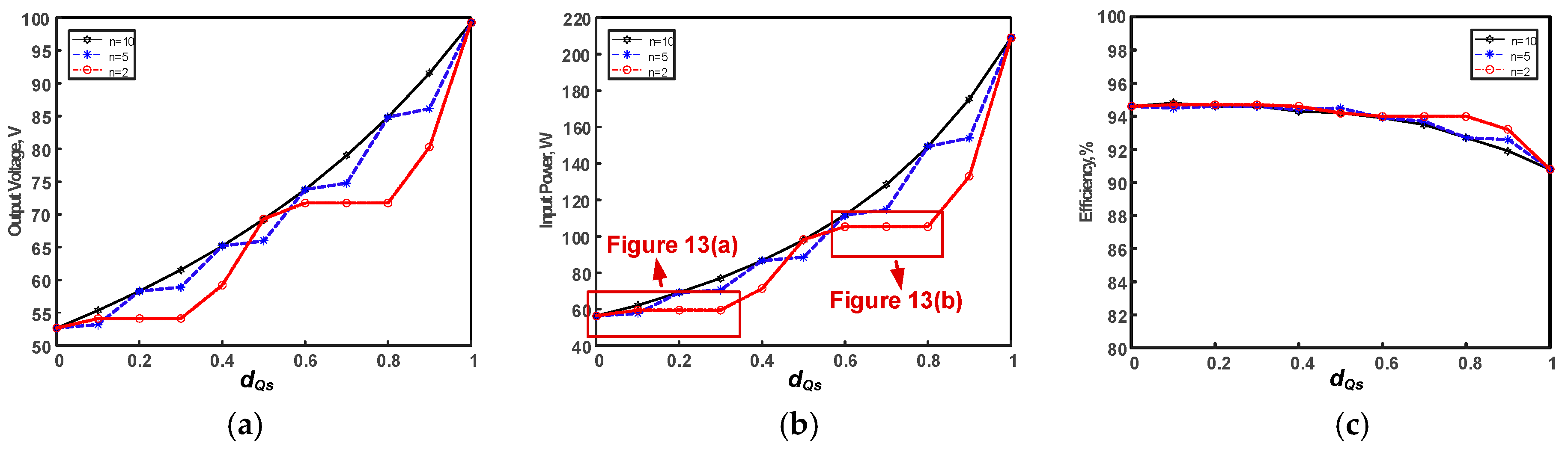
4.2. Equivalent Resistance of SAB and Variation Trend

In Section 3, the equivalent resistance of SAB Ract is regarded as a pure resistance according to the analysis on full-wave rectifier [30] and half-wave rectifier. To validate this assumption, we have Qs working at 8500 Hz with dQs = 0.5. Waveforms of Ip, Is, and Vs are presented in Figure 11. The purple dotted lines show that Ip lags 90° behind Is so sMIp is in phase with Is which conforms to Equation (8). Moreover, the dark dotted lines show that the fundamental voltage Vs and Is are also in phase. These phases verify a purely resistive equivalent impedance.
To further evaluate the impact of frequency ratio n and duty ratio dQs on the system, the simulation results of the output dc voltage, transferred power, and efficiency under different conditions are depicted and compared in Figure 12. Qs works at three frequencies, 8500 Hz (i.e., n = 10), 17,000 Hz (i.e., n = 5), and 42,500 Hz (i.e., n = 2).
From Figure 12a, it is observable that the output voltage grows with the increase of dQs, which verifies the voltage boost function as claimed and also reflects the rise of Rac according to Equation (15). Besides, the increase of input power can prove the negative correlation between Ract and IL as already presented in Equation (6). In addition, it can be observed that the system has the same input power and output voltage once the product of n and dQs is integral and dQs stays the same. The integer of n·dQs means that a switching-ON period of Qs contains an integral multiple of the resonant period, as does the switching-OFF period. On the other hand, an identical dQs means an identical proportion of the on-load time and idle time as presented in Figure 6. Accordingly, the equivalent ac load remains the same. If the switching-ON period of Qs does not contain an integral multiple of the resonant period, the output voltage and input power may rise disproportionately as the blue line and the red line show. This phenomenon occurs because the effective proportions of the on-load time and idle time does not change. The examples in Figure 13 should suffice to demonstrate the stated where n·dQs ≤ 0.5 or 0.5 ≤ n·(1 − dQs) ≤ 1.
Therefore, a large frequency ratio, i.e., a low operation of the receiving side, allows the power to grow in a linear fashion. However, if Qs works at a low frequency, the ripple of the output voltage gets large, which may be unbearable for battery charging. For instance, the system output voltages, input powers, and efficiencies are totally identical when Qs operates at 8500 Hz and 4250 Hz, theoretically. Nevertheless, the ripples at 4250 Hz operation are three times those at 8500 Hz. Thus, there is a trade-off between the system variation linearity and the output ripples considering the practical application. It is worth noting that the switching loss of the MOSFETs is not considered in the simulation, which will rise with the increase of the operating frequency. In this paper, Qs conducts at 8500 Hz as recommended.

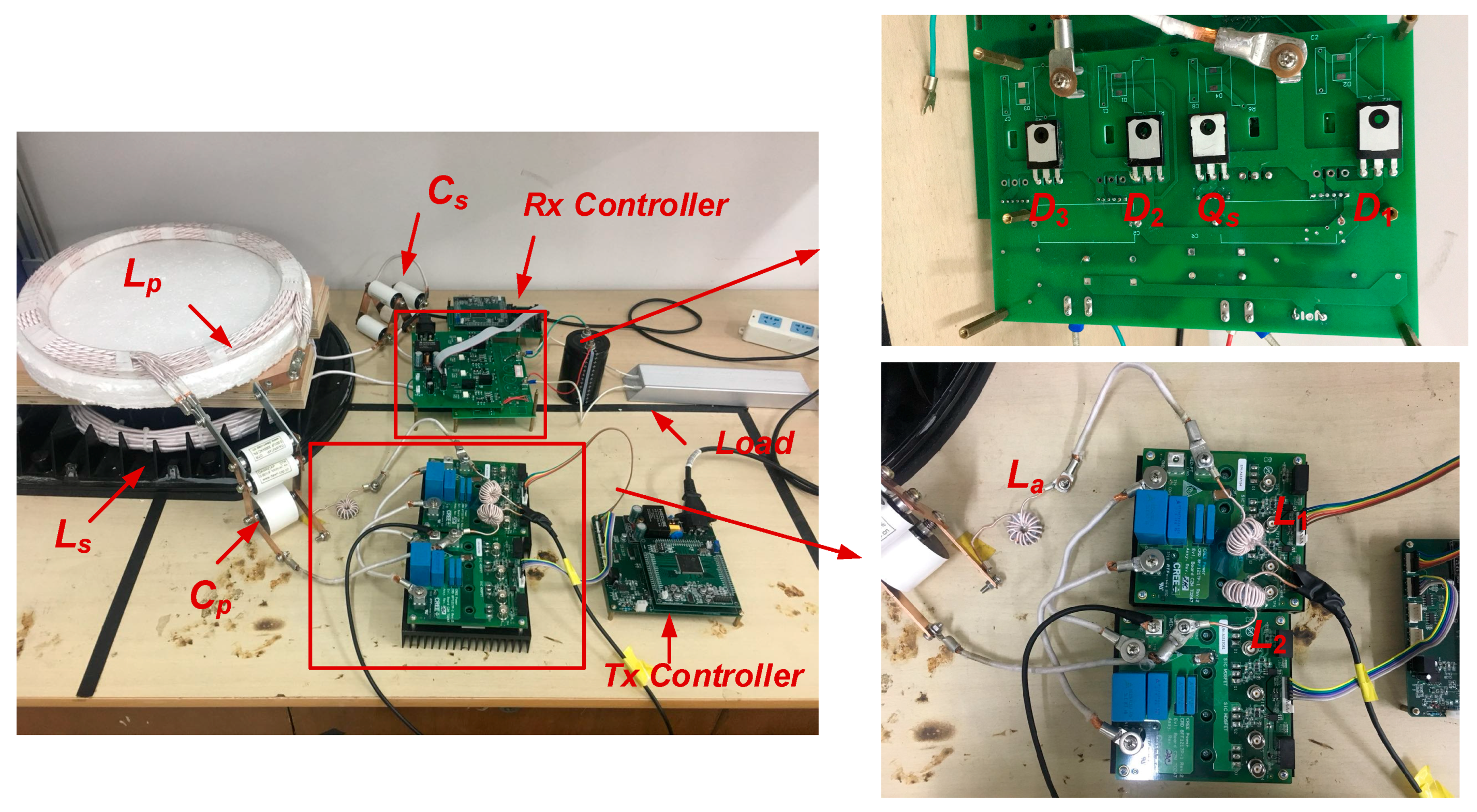
5. Experimental Result and Discussions

To validate and evaluate the aforementioned analyses and simulations, a practical prototype was established and tested. Figure 14 shows the laboratory prototype and its component configurations have been already tabulated in Table 1 in Section 4. However, the actual value of the load was 51.2 Ω and the switching frequencies of the Tx and the Rx were 86 kHz and 8600 Hz, respectively. The DSP TMS320F28335 (San Jose, CA, USA) was used as the digital controller in this system. MPP (Ni-Fe-Mo) cores were chosen for L1, L2, and La for lower loss. The coil diameter is 37 cm and the coil-to-coil gap is set as 10 cm. The inductances are measured by a Keysight E4980AL (Santa Rosa, CA, USA) LCR meter under 86 kHz.

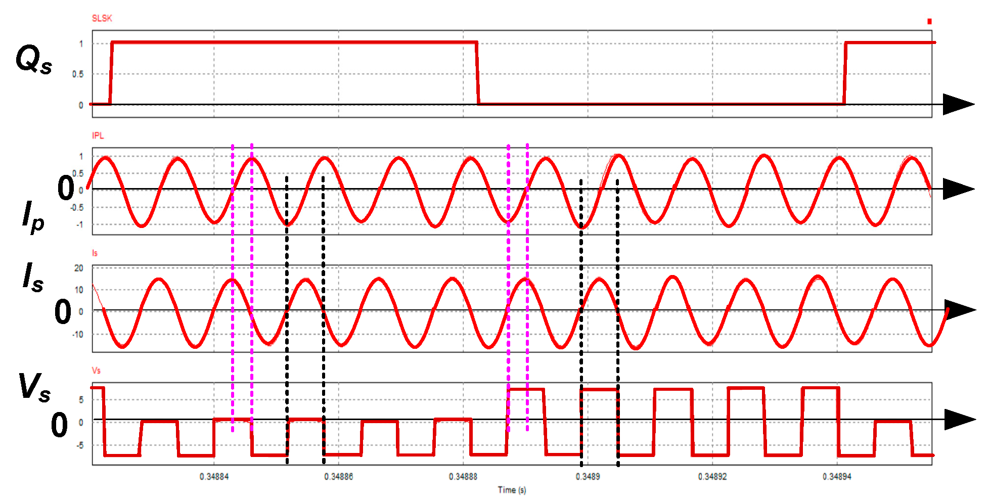
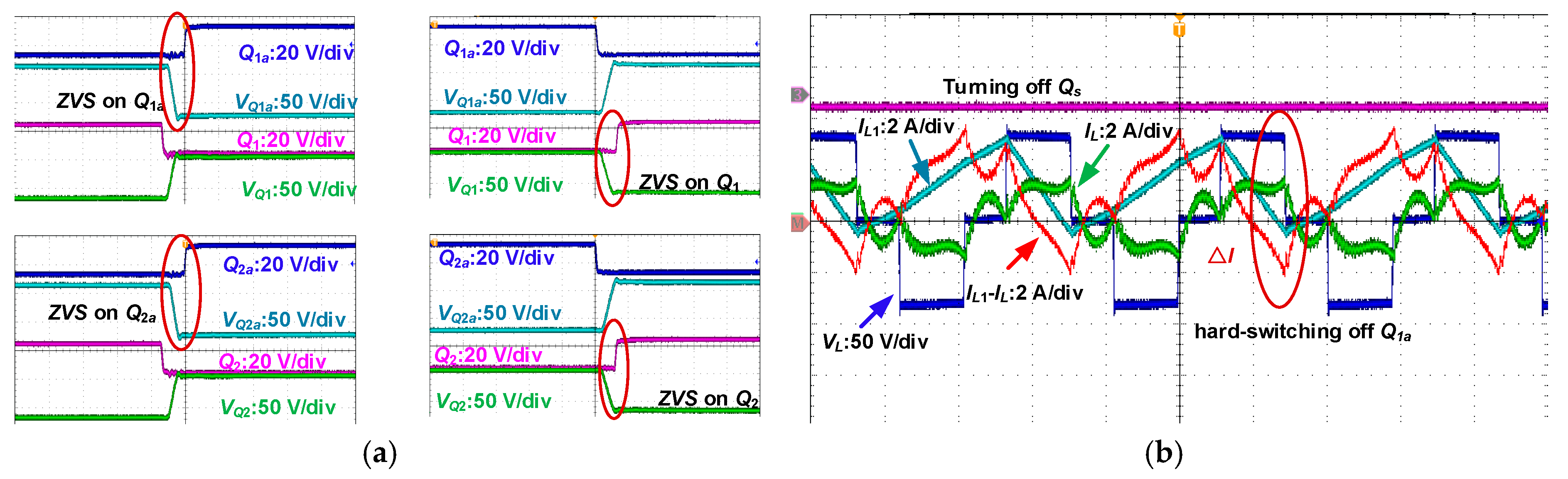
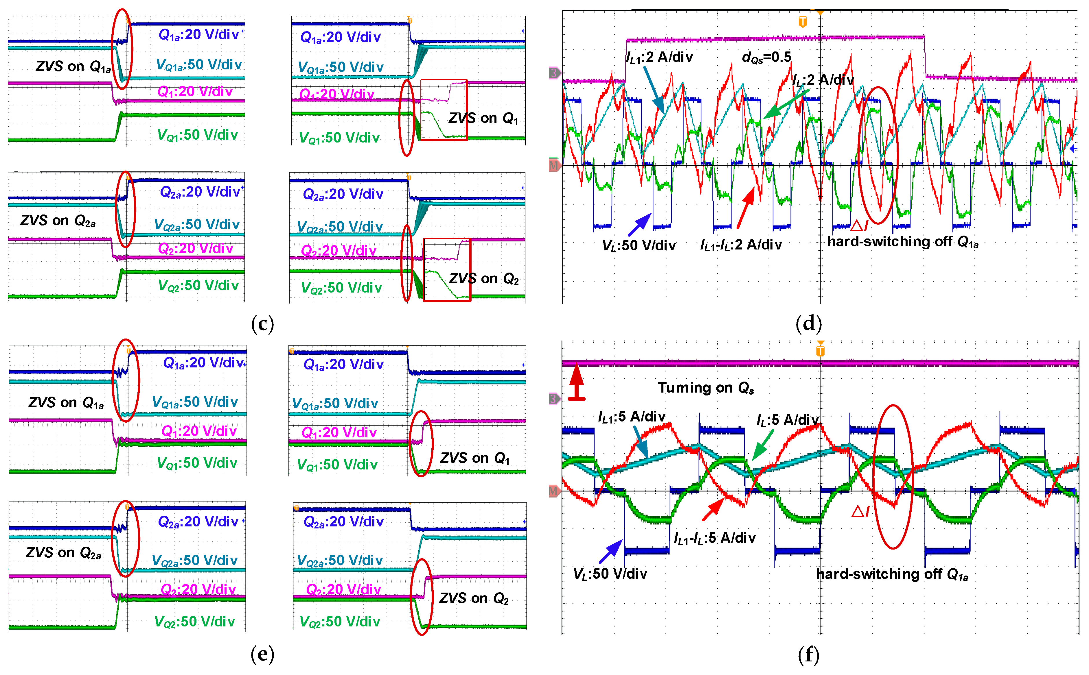
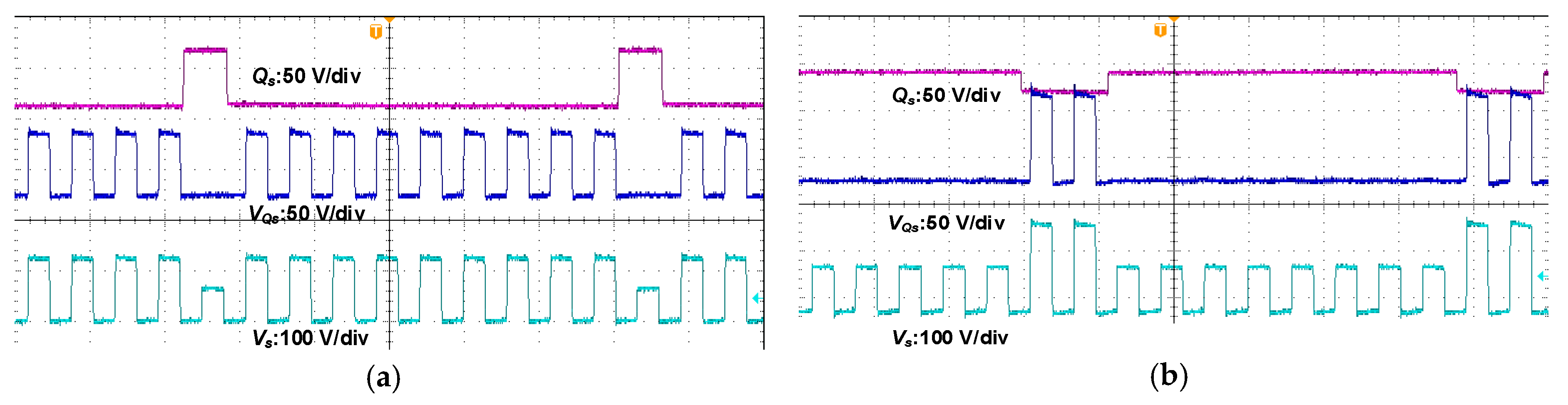
5.1. Soft-Switching Realization

All the four switches on the transmitter can perform ZVS under wide power variation as analyzed. The dead time is set as 2% of the resonant period. The waveforms of the four switches in three cases (Qs stays OFF, dQs = 0.5, and Qs stays ON) are presented in Figure 15. The input power is the smallest when Qs keeps OFF, and the output current IL distorts as claimed in Section 3 and is presented in Figure 15b. Nevertheless, ZVS of the four switches are achieved successfully as presented in Figure 15a. After Qs operates, both the input power and the loaded quality factor rise. When dQs = 0.5, IL is different from each other in every resonant period but IL1 keeps periodic variation. Hence, the current IL1-IL provided for ZVS keeps changing in Figure 15d. However, ZVS of the top-side switches is still realized and ZVS of the bottom-side is also achieved most of the time as illustrated in Figure 15c. When Qs stays on, IL approximates to sine. As can been seen, all the switches can conduct ZVS as presented in Figure 15e. However, the soft switching-OFF for the top side switches is not achieved. The red lines in Figure 15b,d,f denote the result of IL1 minus IL, and the waveforms, when Q1a is going to be turned OFF, are emphasized by the ellipse. At that time, the result △I being negative denotes that there is a current flowing from the source electrode of Q1a to its drain electrode. Therefore, the hard-switching OFF is inevitable.
On the Rx, soft switching of Qs can also be achieved. Figure 16a,b demonstrate the waveforms of Vs and VQs at different dQs conditions. It can be observed that if Qs is turned ON/OFF when Vs is negative and VQs is zero as illustrated in Figure 3c,e, voltage distortion does not occur. Nevertheless, in practice, n·dQs is not always an integer, thereby resulting in three switching situations: Qs hard switching ON, Qs hard switching OFF, and Qs hard switching ON/OFF. To estimate the hard-switching impact, dQs is set as 0.4, and n is set as 10. Then Qs works in soft-switching ON/OFF case as shown in Figure 16c and hard-switching ON/OFF as shown in Figure 16d. When Vs and VQs are positive, Qs is turned ON. The current path switches from Figure 3b to Figure 3d compulsively, leading to a distortion denoted by the ellipse 1 in Figure 16d. When Vs and VQs are positive, Qs is turned OFF. The current path switches from Figure 3d to Figure 3b compulsively, leading to a distortion denoted by the ellipse 2 in Figure 16d. It is found that when the input power is 103.2 W, the former efficiency is 93.3%, a little higher than the latter efficiency of 92.7%, saving switching loss of 0.5 W.
Additionally, IL1 is observed to analyze the impact of the equivalent load and the front-end inductance. At first, the value of L1 and L2 is set as 51 μH. When Qs stays OFF, both the input power and the equivalent impedance are small. The inductance, 51 μH, is much less than the proposed value, 107 μH. Part of IL1 is below zero as depicted in Figure 17a, thereby showing a circulating current exists in L1 and L2. However, with the increase of the equivalent impedance, the value of 51 μH meets the requirements. Hence, the circulating current is eliminated and IL1 is always above zero as presented in Figure 17b,c.

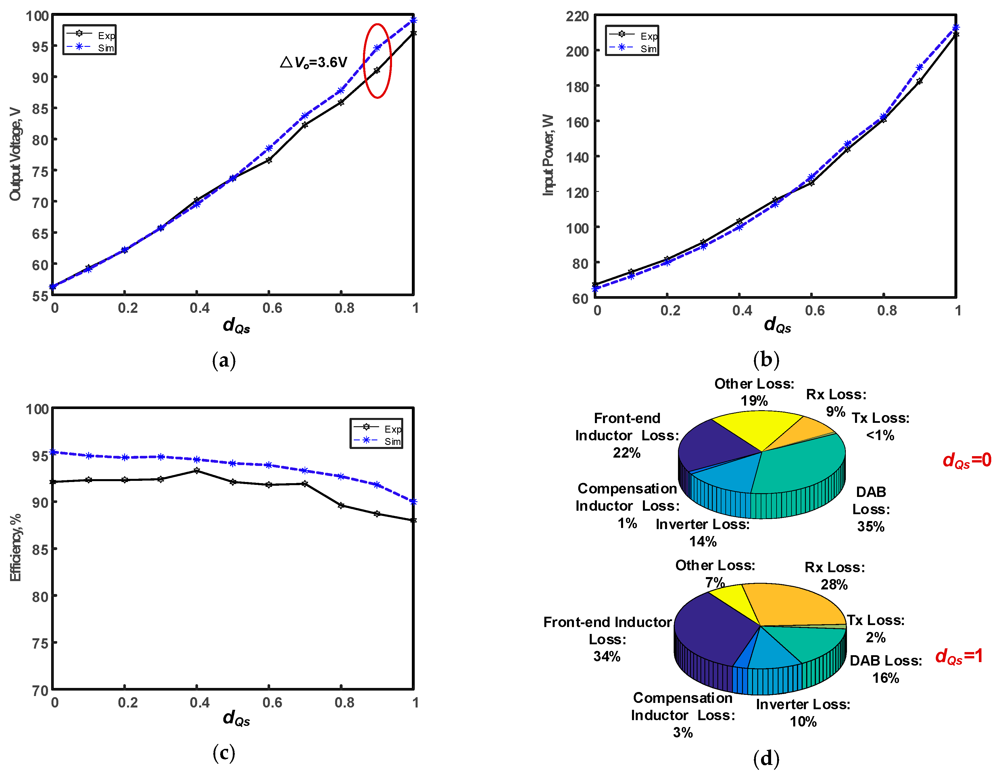
5.2. Efficiency and Loss Estimation
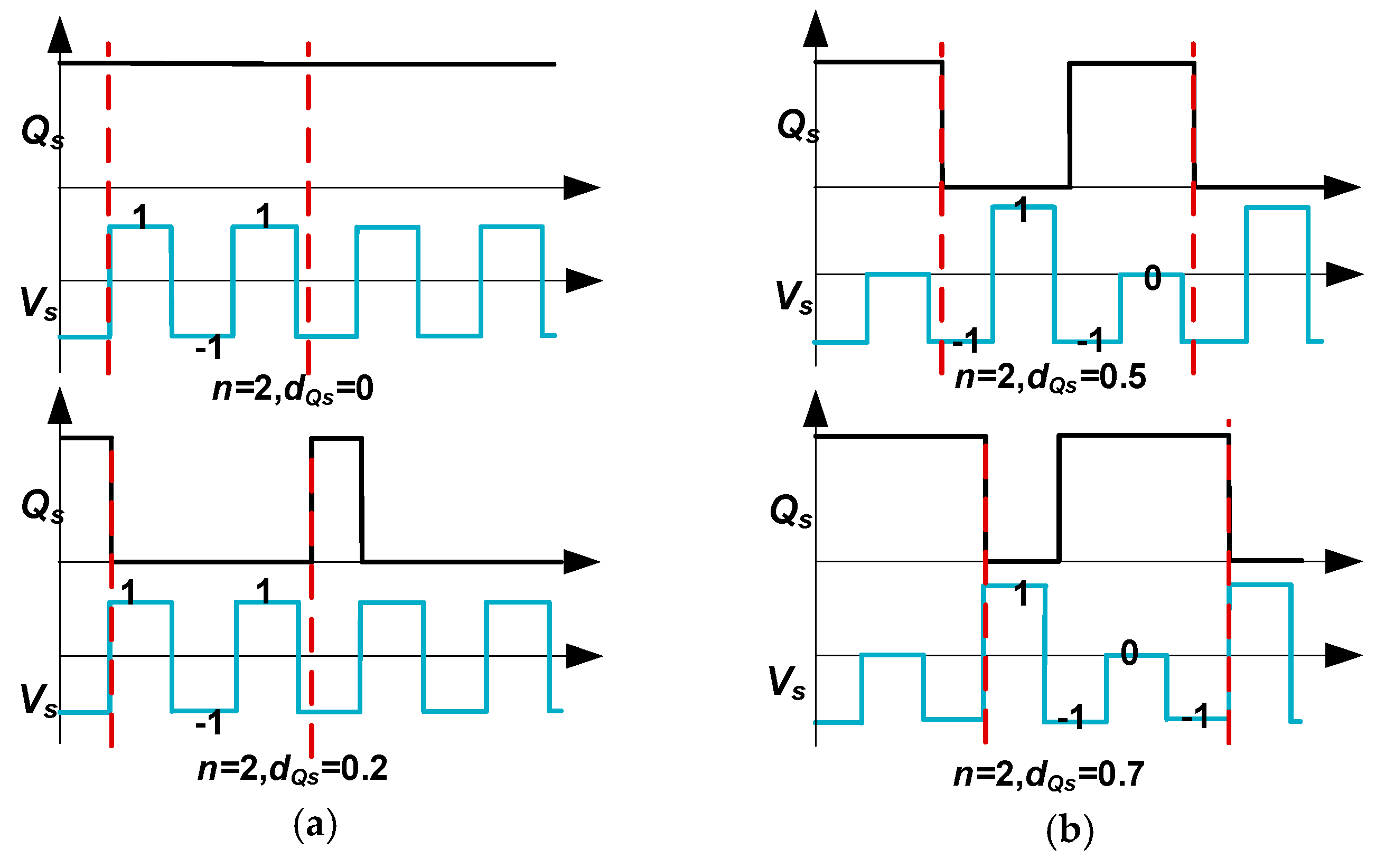
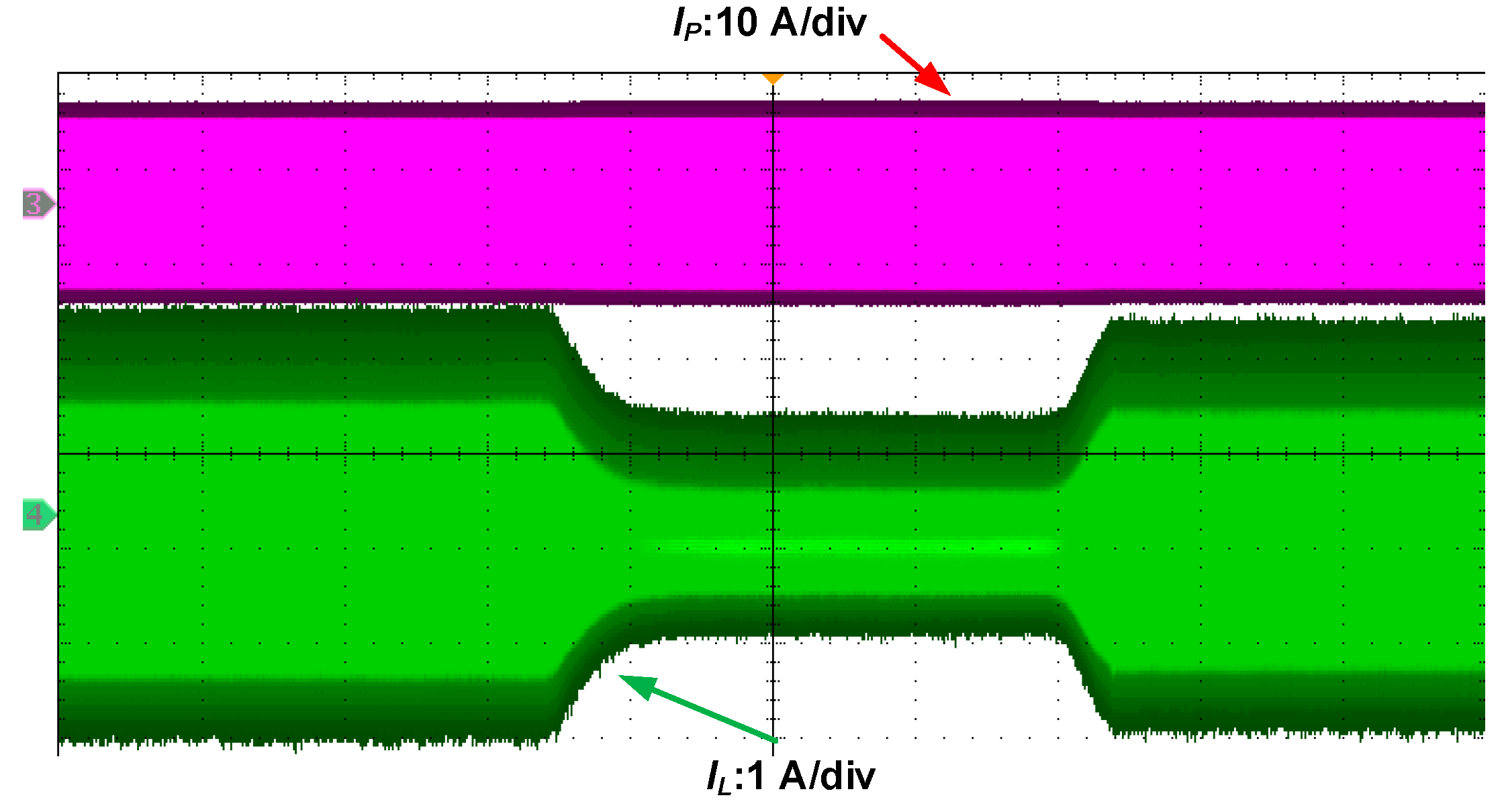
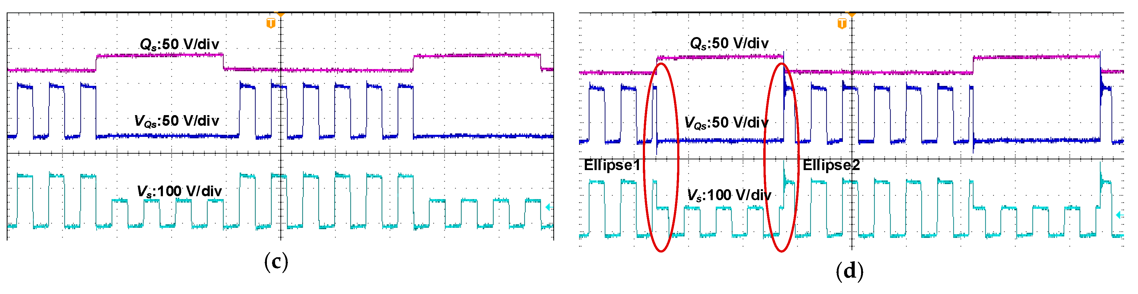
Figure 18 demonstrates the system efficiency and the loss estimation. The blue dashed line presents the simulation result and the dark line presents the experimental result. Figure 18a shows that a higher output voltage more than the input voltage 24 V, is accomplished and boosted further after Qs working. The results support the calculation of Equation (16). The experimental output voltage at the beginning is the same as the simulation but deviates from the theoretical value with the increasing of dQs and system operation power. Besides, the input power of the experiment is a little higher than that of the simulation power when dQs is below 0.5, whereas this situation reverses after dQs becomes above 0.5. This difference is mainly caused by the modelling of the SAB in the simulations. At first, the practical forward voltage drop is not invariably 0.6 V but increase from 0.6 V to 0.8 V. The deterioration of the voltage drop can be regarded as the increase of Ract, thereby decreasing the practical input power according to Equation (17). In addition, the input current surging from 2.8 A to 8.7 A and the temperature rise may result in the parameter drift and the difference presented in Figure 18. High efficiency is achieved over the variation of dQs as depicted in Figure 18c. Although the efficiency drops with dQs rising, 88% efficiency is sustained. In general, the results of the established simulation and experimental prototype are accordant and validate the proposed topology and methods. High efficiency can still be obtained though three inductors are added into the WPT system.
Based on the data presented in Figure 18a,b, the power losses can be calculated. When Qs stays OFF, the power loss is 5.31 W, where the losses caused by the rectifier (0.6 V drop) and the inner resistance of the front-end inductors L1 and L2 (0.2 Ω) are obvious and make the main percentage as presented in Figure 18d, where dQs is 0. After Qs operates and the power transfer rate rises, the loss ratio of the front-end inductors and the Rx coil increases as shown in Figure 18d where dQs is 1. Hence, there are two ways to improve the system efficiency. One is decreasing the high-frequency resistance by optimizing the inductors and determining a proper value according to Equations (21) and (25). Another method is reducing the receiver coil resistance with optimal coil manufacturing. Otherwise the output rate reduces according to Equations (16) and (17).

5.3. Load Tripping

To further present the advantage of LCL topology to the load tripping as aforementioned, experiments are added for validation. For convenience, the Tx coil will be artificially removed to imitate the load tripping scenario. Figure 19 shows the variation of IL and IP. Over the working time, IP stays constant even though the load is off, which is in accordance with the analysis of Equation (7). However, IL varies when the load is off and on. IL becomes small when the load is off, but becomes large again when the load is reconnected. Moreover, it can be seen that the whole system remains safe all the time.

6. Conclusions

The LCL topology is regarded as an ideal network used in the WPT systems due to its constant resonant current in the Tx coil and independence of the reflected impedance of the receivers. However, this topology requires a large source voltage to generate transmitting current and induced voltage of receivers, which limits its application in the low voltage scenarios, such as 12~24 V. This paper applied a CFI into WPT systems to boost the voltage for LCL. ZVS of the switches were accomplished under wide range of power rates and also under serious current distortion. The ability of the CFI to turn OFF the top-side switches softly was also deduced and presented in this paper.
On the receiving side, a SAB was proposed and applied to regulate and boost the output voltage and the system power. The SAB allows a lower frequency and reduces the communication requirement compared with the DAB synchronization. Higher output voltage and wide variation range were accomplished.
Guidelines on the parameter design of the front-end inductance, coils and optimal load were elaborately presented. Although more inductors were added into the system, a peak efficiency of 93.3% was obtained and the lowest efficiency was maintained at 88% with proper configuration. Both simulations and experimental results are conducted to verify the aforementioned analysis. Furthermore, optimization methods for efficiency improvement is included in this study.

Author Contributions

H.T., X.Y., and T.W. conceptualized the main idea of this research project; T.W. designed and conducted the experiments with the help of M.A. and X.L.; T.W., X.L., and N.J. checked and analyzed the results. T.W. wrote the whole paper; M.A. reviewed and edited the paper.

Funding

This work was funded by United Foundation of NSFC-Henan (U1604136).

Conflicts of Interest

The authors declare no conflict of interest.

References

  1. Asheer, S.; Al-Marawani, A.; Khattab, T.; Massoud, A. Inductive power transfer with wireless communication system for electric vehicles. In Proceedings of the 2013 7th IEEE GCC Conference and Exhibition, Doha, Qatar, 17–20 November 2013; pp. 517–522. [Google Scholar]
  2. Musavi, F.; Eberle, W. Overview of wireless power transfer technologies for electric vehicle battery charging. IET Power Electron. 2014, 7, 60–66. [Google Scholar] [CrossRef]
  3. Song, K.; Zhu, C.; Kim Ean, K.; Imura, T.; Hori, Y. Wireless power transfer for running EV powering using multi-parallel segmented rails. In Proceedings of the 2015 IEEE PELS Workshop on Emerging Technologies: Wireless Power, Daejeon, Korea, 5–6 June 2015. [Google Scholar]
  4. Yin, N.; Xu, G.; Yang, Q.; Zhao, J.; Yang, X.; Jin, J.; Fu, W.; Sun, M. Analysis of wireless energy transmission for implantable device based on coupled magnetic resonance. IEEE Trans. Magn. 2012, 48, 723–726. [Google Scholar] [CrossRef]
  5. Ma, A.; Poon, A.S.Y. Midfield wireless power transfer for bioelectronics. IEEE Circuits Syst. Mag. 2015, 15, 54–60. [Google Scholar] [CrossRef]
  6. Huang, C.Y.; Boys, J.T.; Covic, G.A. LCL pickup circulating current controller for inductive power transfer systems. IEEE Trans. Power Electron. 2013, 28, 2081–2093. [Google Scholar] [CrossRef]
  7. Qu, X.; Han, H.; Wong, S.C.; Chi, K.T.; Chen, W. Hybrid IPT topologies with constant current or constant voltage output for battery charging applications. IEEE Trans. Power Electron. 2015, 30, 6329–6337. [Google Scholar] [CrossRef]
  8. Zhang, W.; Wong, S.C.; Chi, K.T.; Chen, Q. Analysis and comparison of secondary series- and parallel-compensated inductive power transfer systems operating for optimal efficiency and load-independent voltage-transfer ratio. IEEE Trans. Power Electron. 2014, 29, 2979–2990. [Google Scholar] [CrossRef]
  9. Ge, S.; Liu, C.; Li, H.; Guo, Y.; Cai, G.W. Double-LCL resonant compensation network for electric vehicles wireless power transfer: Experimental study and analysis. IET Power Electron. 2016, 9, 2262–2270. [Google Scholar]
  10. Sohn, Y.H.; Choi, B.H.; Lee, E.S.; Lim, G.C.; Cho, G.H.; Rim, C.T. General unified analyses of two-capacitor inductive power transfer systems: Equivalence of current-source SS and SP compensations. IEEE Trans. Power Electron. 2015, 30, 6030–6045. [Google Scholar] [CrossRef]
  11. Tan, L.; Pan, S.; Xu, C.; Yan, C.; Liu, H.; Huang, X. Study of constant current-constant voltage output wireless charging system based on compound topologies. J. Power Electron. 2017, 17, 1109–1116. [Google Scholar]
  12. Li, S.; Li, W.; Deng, J.; Nguyen, T.D.; Mi, C.C. A double-sided LCC compensation network and its tuning method for wireless power transfer. IEEE Trans. Veh. Technol. 2015, 64, 2261–2273. [Google Scholar] [CrossRef]
  13. Xiao, C.; Cheng, D.; Wei, K. An LCC-C compensated wireless charging system for implantable cardiac pacemakers: Theory, experiment, and safety evaluation. IEEE Trans. Power Electron. 2018, 33, 4894–4905. [Google Scholar] [CrossRef]
  14. Dai, X.; Li, W.; Li, Y.; Su, Y.; Tang, C.; Wang, Z.; Sun, Y. Improved LCL resonant network for inductive power transfer system. In Proceedings of the 2015 IEEE PELS Workshop on Emerging Technologies: Wireless Power (WoW), Daejeon, Korea, 5–6 June 2015. [Google Scholar]
  15. Peng, F. Z-source inverter. IEEE Trans. Ind. Appl. 2003, 39, 504–510. [Google Scholar] [CrossRef]
  16. Zeng, H.; Peng, F.Z. SiC based Z-source resonant converter with constant frequency and load regulation for EV wireless charger. IEEE Trans. Power Electron. 2017, 32, 8813–8822. [Google Scholar] [CrossRef]
  17. Siwakoti, Y.P.; Town, G. Improved modulation Technique for voltage fed quasi-Z-source DC/DC converter. In Proceedings of the 2014 IEEE Applied Power Electronics Conference and Exposition (APEC), Fort Worth, TX, USA, 16–20 March 2014; pp. 1973–1978. [Google Scholar]
  18. Wang, T.; Liu, X.; Tang, H.; Ali, M. Modification of the wireless power transfer system with Z-source inverter. IET Electron. Lett. 2017, 53, 106–108. [Google Scholar] [CrossRef]
  19. Shen, M.; Peng, F. Operation modes and characteristics of the Z-source inverter with small inductance or low power factor. IEEE Trans. Ind. Electron. 2008, 55, 89–96. [Google Scholar] [CrossRef]
  20. Sha, D.; You, F.; Wang, X. A high-efficiency current-fed semi-dual-active bridge DC-DC converter for low input voltage applications. IEEE Trans. Ind. Electron. 2016, 63, 2155–2164. [Google Scholar] [CrossRef]
  21. Sha, D.; Wang, X.; Chen, D. High efficiency current-fed dual active bridge DC-DC converter with ZVS achievement throughout full range of load using optimized switching patterns. IEEE Trans. Power Electron. 2018, 33, 1347–1357. [Google Scholar] [CrossRef]
  22. Fu, M.; Zhang, T.; Ma, C.; Zhang, X. Efficiency and optimal loads analysis for multiple-receiver wireless power transfer systems. IEEE Trans. Microw. Theory Tech. 2015, 63, 801–812. [Google Scholar] [CrossRef]
  23. Liu, X.; Wang, T.; Yang, X.; Jin, N.; Tang, H. Analysis and design of a wireless power transfer system with dual active bridges. Energies 2017, 10, 1588. [Google Scholar] [CrossRef]
  24. Sanborn, G.; Phipps, A. Standards and methods of power control for variable power bidirectional wireless power transfer. In Proceedings of the 2017 IEEE Wireless Power Transfer Conference (WPTC), Taipei, Taiwan, 10–12 May 2017. [Google Scholar]
  25. Sha, D.; Wang, X.; Xu, Y. Unequal PWM control for a current-fed DC-DC converter for battery application. In Proceedings of the 2017 IEEE Applied Power Electronics Conference and Exposition (APEC), Tampa, FL, USA, 26–30 March 2017; pp. 3373–3377. [Google Scholar]
  26. Kazimierczuk, M.K. Boost PWM DC-DC converter. In Pulse-Width Modulated DC-DC Power Converters, 2nd ed.; John Wiley & Sons, Wright State University: Dayton, OH, USA, 2017; Chapter 3; pp. 85–137. [Google Scholar]
  27. Mai, R.; Liu, Y.; Li, Y.; Yue, P.; Cao, G.; He, Z. An active rectifier based maximum efficiency tracking method using an additional measurement coil for wireless power transfer. IEEE Trans. Power Electron. 2018, 33, 716–728. [Google Scholar] [CrossRef]
  28. Liu, X.; Wang, T.; Yang, X.; Tang, H. Analysis of efficiency improvement in wireless power transfer system. IET Power Electron. 2018, 11, 302–309. [Google Scholar] [CrossRef]
  29. Yang, E.X.; Lee, F.C.; Jovanovic, M.M. Small-signal modeling of series and parallel resonant converters. In Proceedings of the 1992 Applied Power Electronics Conference and Exposition (APEC), Boston, MA, USA, 23–27 February 1992; pp. 785–792. [Google Scholar]
  30. Zhang, Y.; Chen, K.; He, F.; Zhao, Z.; Lu, T.; Yuan, L. Closed-form oriented modeling and analysis of wireless power transfer system with constant-voltage source and load. IEEE Trans. Power Electron. 2016, 31, 3472–3481. [Google Scholar] [CrossRef]
Figure 1. Proposed circuit diagram of WPT systems with one receiver.
Electronics 07 00178 g001
Figure 2. (a) Typical operation patterns of the CFI, (b) t1~t2; (c) t3~t4; (d) t5~t6; (e) t7~t8.
Electronics 07 00178 g002
Figure 3. Typical waveforms and operation patterns of the SAB (a) waveforms of the SAB (b) current path when Qs is OFF and Is is positive (c) current path when Qs is OFF and Is is negative (d) current path when Qs is ON and Is is positive (e) current path when Qs is ON and Is is negative.
Electronics 07 00178 g003
Figure 4. Current paths for CFI conducting ZVS (a) state before Q1a is on t0~t1; (b) state before Q1 is on t2~t3.
Electronics 07 00178 g004
Figure 5. Current paths before turning OFF Q1a (a) preclude to the hard OFF; (b) preclude to the soft OFF.
Electronics 07 00178 g005
Figure 6. Difference of Vs caused by the switch time (a) Qs switch time; (b) distortion of Vs; (c) ideal waveform of Vs.
Electronics 07 00178 g006
Figure 7. Equivalent circuit diagram.
Electronics 07 00178 g007
Figure 8. Typical waveforms of the Rx under different duty ratios (a) dQs = 0; (b) dQs = 1.
Electronics 07 00178 g008
Figure 9. Typical waveforms of the CFI.
Electronics 07 00178 g009
Figure 10. Typical waveforms of Q1a and IL1 with a same L but different dQs: (a) R = 52 Ω, dQs = 0, η = 94.5%; (b) R = 52 Ω, dQs = 0.5, η = 94.1%; (c) R = 52 Ω, dQs = 1, η = 90.8%; (d) R = 20 Ω, dQs = 1.
Electronics 07 00178 g010
Figure 11. Phase differences in the Tx.
Electronics 07 00178 g011
Figure 12. System performance under different frequencies and duty ratios (a) output voltage (b) input power (c) efficiency.
Electronics 07 00178 g012
Figure 13. Impact of n and dQs on the equivalent impedance when n·dQs is small (a) n·dQs ≤ 0.5 (b) 0.5 ≤ n·(1 − dQs) ≤ 1.
Electronics 07 00178 g013
Figure 14. Prototype of the proposed system.
Electronics 07 00178 g014
Figure 15. ZVS waveforms under different cases: (a) ZVS of four switches when dQs = 0; (b) current waveforms when dQs = 0; (c) ZVS of four switches when dQs = 0.5; (d) current waveforms when dQs = 0.5 (e) ZVS of four switches when dQs = 1; (f) current waveforms when dQs = 1.
Electronics 07 00178 g015aElectronics 07 00178 g015b
Figure 16. Waveforms of Vs and VQs with different dQs: (a) dQs = 0.1 (b) dQs = 0.8 (c) dQs = 0.4 (d) dQs = 0.4 but hard switching.
Electronics 07 00178 g016aElectronics 07 00178 g016b
Figure 17. Waveforms of IL1, Vp, and Vs: L1 is 51 μH but the equivalent impedance Ract changes (a) Qs stays OFF, Ract reaches the maximum, part of IL1 is below zero; (b) Qs stays ON, Ract reaches the minimum, IL1 is above zero; (c) Qs operates with dQs = 0.5, IL1 is above zero.
Electronics 07 00178 g017
Figure 18. Efficiency and power loss comparison (a) Vo vs. dQs; (b) Pi vs. dQs; (c) η vs. dQs; (d) loss analysis of extreme working cases.
Electronics 07 00178 g018
Figure 19. Waveforms of IL and IP when load tripping occurs.
Electronics 07 00178 g019
Table 1. Model Parameters.
ParameterValueParameterValue
Load R52 ΩInput voltage EV24 V
Transmitting switching frequency fs85 kHzMutual inductance M18 μH
Transmitting inductance Lp15.5 μHTransmitting inner resistance rp8 mΩ
Receiving inductance Ls274.7 μHReceiving inner resistance rs0.3 Ω
Compensation inductance La15.5 μHCompensation inner resistance rLa0.04 Ω
DC inductance L1 & L251 μHDC inner resistance rL0.2 Ω
Transmitting capacitance Cp222 nFReceiving capacitance Cs12.8 nF
Clamp capacitance Co470 μFTransmitting duty ratio dS0.7
Forward voltage drop of diode VF0.6 VOn resistance of MOSFET Ron80 mΩ

