Abstract
A broadband switch-less bi-directional low noise amplifier based on negative group delay (NGD) matching circuits with a non-Foster characteristic is proposed. To validate the feasibility, two circuits were designed and compared, which are matched by NGD circuits and traditional lumped elements respectively. The structure proposed in this paper has a measured relative bandwidth (RBW) of 32.6% rather than 5.1% for the traditional one. From 797 MHz to 1095 MHz, the input and output return losses (RL) are more than 10 dB with a noise factor (NF) of about 3.5 dB and peak gain of 12.2 dB. Meanwhile, the reverse isolation and stability factor (SF) are greater than 20 dB and 1, respectively. The group delay (GD) value is 0.5 ns ± 0.25 ns in the operating frequency band, which is much flatter and lower compared to that of the traditional one.
1. Introduction
In recent years, wireless communication systems have been rapidly developed, in which amplifiers are required to improve system performance. Since wireless systems are preferably designed for small size, the reuse of amplifiers is widely adopted to reduce the number of devices. Therefore, the designs of bi-directional amplifiers are concerned by researchers. In this case, there are some structures to create a bi-directional amplifier [1,2]. However, the additional transmitter/receiver (T/R) switches in the amplifier result in large size and significant losses. For overcoming these weaknesses, methods to eliminate the switch have been put forward [3,4,5,6,7]. In Reference [3], the switches were placed within the bias circuit to achieve a compact structure. However, the operating bandwidth was narrow and it was difficult to simultaneously optimize the matching network in both forward- and reverse-paths. To reduce the design complexity of the matching network, some methods were presented in References [4,5,6]. Nevertheless, only the interconnected network at the input and output terminals has been considered, while the amplifier itself is ignored. Since the input- and output-port impedance of the single amplifier is not flat, the operating band of the bi-directional amplifier cannot be wide. In Reference [7], resistors were added to a matching network to increase the input and output return losses (RL). However, the bi-directional amplifier [7] still suffers from a narrow bandwidth. To improve the bandwidth, distributed bi-directional amplifiers were proposed [8], but the structure was so complex that it was oversized. Therefore, it could not be applied to miniaturized equipment. To achieve broadband matching, and maintain a small size, non-Foster reactive elements can be used [9]. The traditional methods for realizing the non-Foster reactive elements, in general, rely on active devices (i.e., negative impedance converters and negative impedance inverters), which are susceptible to instability [10]. Recently, a new method to achieve negative capacitance, and inductance with negative group delay (NGD) networks, was proposed [11]. NGD networks can be classified as passive and active circuits. Passive NGD circuits can be implemented by using RLC resonators [11,12], finite unloaded quality-factor resonators [13], the feedback loop technique [14], or signal interference techniques [15,16]. There is loss generated in the NGD networks. Usually, amplifiers are adopted to compensate for this loss. The NGD circuits including amplifiers is the active NGD circuits [17,18,19]. Among existing NGD circuits, passive NGD circuits based on RLC resonators are more suitable for matching networks. In this paper, a modified NGD circuit composed of an RLC resonator is proposed to achieve broadband matching of a switch-less bi-directional amplifier. At the same time, the NGD effect can be used to compensate for the positive delay generated by the rest of the amplifier, so that the overall delay of the bi-directional amplifier is decreased. Compared to the amplifier with traditional lumped elements, the group delay (GD) becomes flatter. This paper is organized as follows: the NGD circuits used as matching networks are analyzed in Section 2, in Section 3 a switch-less bi-directional low noise amplifier with NGD matching network is presented, Section 4 discusses the results of simulations and measurements, and conclusions are drawn in Section 5.
2. Analysis of Matching Network for Low Noise Amplifier
In this work, the ATF-54143 field-effect transistor (FET) was used to design a low noise amplifier operating at 0.915 GHz. The amplifier was simulated using Advanced Design System version 2011. The traditional L-type matching networks (series inductors and shunt capacitors) were used to achieve matching. The input and output impedance curves after matching are shown in Figure 1. It is seen that the impedance of the real part is only matched to 50 Ω and the imaginary part is matched to 0 at the center frequency of 0.915 GHz and their fluctuation was obvious. Therefore, the matching bandwidth was narrow.
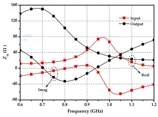
Figure 1.
Impedance curves of the amplifier matched with the traditional method.
In order to improve the matching bandwidth of the amplifier, non-Foster elements are needed. In recent years, non-Foster elements implemented by NGD circuits were proposed in References [20,21]. Figure 2a,b gives the traditional configurations of NGD circuits. The non-Foster characteristic can be obtained using these two configurations or their combinations. Compared to the second configuration, the first configuration is easier to connect with the microstrip line; thus, it is more suitable for the microstrip matching network.
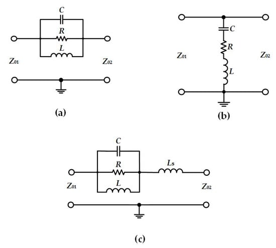
Figure 2.
Schematics of the (a) original parallel NGD (negative group delay) circuit, (b) original series NGD circuit, and (c) modified NGD circuit.
It can be established that the series impedance of the NGD circuit shown in Figure 2a is:
S21 can be obtained as:
where Z01 and Z02 are the input- and output-port impedances, respectively.
According to Equations (1) and (2), the S21 can be further deduced as:
where Ra and Xa are the real and imaginary part of Za, respectively. Subsequently, the phase can be derived as:
By solving the differential of phase, the expression of group delay can be obtained as:
where U and V are the differential coefficients of Ra and Xa, respectively. The expressions of U and V are shown in Equations (6) and (7).
Through analysis, if a negative group delay is required, the following conditions must be satisfied:
As can be seen from Equation (1), only a negative capacitance was obtained under the conditions of Equation (9).
The calculated values of Ca with R = 22 Ω for 0.915 GHz are shown in Figure 3a. It is observed that some negative capacitance could not be realized. For example, when the input impedance of the FET was 35.7 − j22.5 Ω at 0.915 GHz, the expected negative capacitance was −7.7 pF for the impedance matching, but the realizable range of the negative capacitance was from −60 pF to −15.5 pF. Therefore, a series inductor was inserted into the NGD circuit to ensure the realization of the expected negative capacitance, as shown in Figure 3b, with R = 22 Ω and Ls = 2.6 nH. The series impedance of the modified NGD circuit was obtained as:
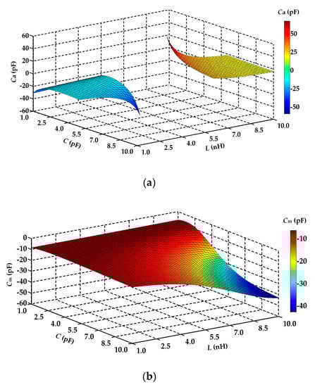
Figure 3.
The values of the capacitance: (a) Ca and (b) Cm.
Furthermore, the modified NGD circuit was required to satisfy Equation (11) to achieve impedance matching.
where M is the real part of the port impedance of the FET and N (N < 0) is the imaginary part. Therefore, the compensation of the imaginary part and the matching of the real part can both be achieved. As long as proper values of the lumped elements are selected, a suitable negative capacitance with the NGD characteristic can be obtained.
As there are four unknown quantities, but only two equations (Equations (8) and (11)); the values cannot be obtained directly. Therefore, Taguchi optimization [22] is applied. C, R, L, and Ls are optimization variables with the optimization objective of Eqautions (12) and (13).
In order to obtain the NGD characteristic, Equation (8) was also used as a condition for the end of the iteration. After a finite number of iterations, the values of lumped elements could be obtained.
3. Design of Switch-Less BDLNA
A schematic of the proposed switch-less bi-directional low noise amplifier is shown in Figure 4. Two low noise amplifiers are loop-back-connected using transmission lines with the characteristic impedance of Z0 = 50 Ω. The direction of amplification could be controlled by reversing the direct current (DC) voltage of FET ① and FET ②. When FET ① is working, isolation is obtained by keeping FET ② in the deep pinch-off region, and vice versa. The specific working status is shown in Table 1.
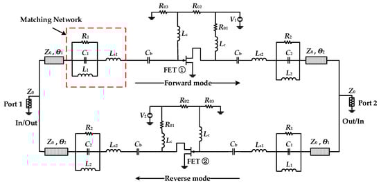
Figure 4.
Schematic of the proposed switch-less bi-directional low-noise amplifier.

Table 1.
Working status.
In order to make sure that one path is not affected by the other path, the overall input and output impedance was considered, which was revealed by the single amplifier in the ON and OFF modes. The specific method makes the input- and output-port impedances of the amplifier in the OFF mode as close as possible to the open-circuit impedance. This is achieved by employing a one-section transmission line of appropriate electrical length [6] so that the ON-mode amplifier, operating in the active region (VDC = 5 V), is matched by the modified NGD circuit to the 50 Ω impedance at the input, as well as output, ports, while the OFF-mode amplifier (VDC = 0 V) provides a high impedance at two ports. Furthermore, the static working point of the ON-mode amplifier was selected to be 3 V, with 60 mA, so the bias resistors were R01 = 68 Ω, R02 = 430 Ω and R03 = 51 Ω. The blocking capacitor Cb and choke inductor Lc were 15 pF and 47 nH, respectively.
Due to the need to combine forward and reverse paths, the flatness of port impedance generated by a single amplifier was significant. If the impedance could be kept constant in a broadband, the optimizations, that focus on impedance matching after forward and reverse paths are combined, will be easy.
In order to simplify the design of the matching circuit, the impedance of the matching network was selected according to the input impedance of the port, instead of the minimum noise. For the input port, the impedance of FET was 35.7 − j22.5 Ω. Optimized using the Taguchi algorithm, the values of elements in the modified NGD circuit were obtained as R1 = 22 Ω, L1 = 4.5 nH, C1 = 1.6 pF, Ls1 = 2.6 nH. The value of GD generated by the modified NGD circuit is given in Figure 5. The NGD time was −30 ps at 0.915 GHz. Therefore, the modified NGD circuit cannot only be used to achieve impedance matching, but also can compensate for the positive group delay.
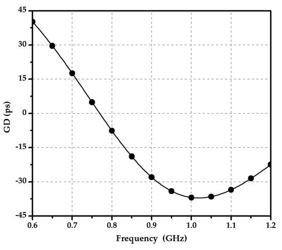
Figure 5.
GD (group delay) generated by the input matching circuit.
Similarly, the matching circuit at the output port can be obtained for the impedance (35.4 − j29.2 Ω) of FET. Therefore, the values of the elements were achieved as R2 = 20 Ω, L2 = 3.3 nH, C2 = 8.2 pF, Ls2 = 4.7 nH.
The impedance curves of the input and output after matching with the proposed method are given in Figure 6. Compared with the curves in Figure 1, it is obvious that a flatter impedance can be obtained by using the modified NGD circuit. Therefore, the matching bandwidth can be broadened.
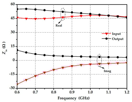
Figure 6.
Impedance curves of the amplifier matched with the proposed method.
4. Manufacturing and Measurements
To validate the proposed method, two switch-less BDLNAs were designed to operate at 0.915 GHz. The circuits were implemented on a 1.5-mm-thick FR-4 substrate with a relative permittivity of 4.4. The amplifiers were measured using a vector network analyzer and a noise figure analyzer. A photograph of the traditional BDLNA, using the L-type matching network, is shown in Figure 7a and that of the proposed one, using NGD matching network, is shown in Figure 7b. The characteristic impedance of the meander microstrip line is 50 Ω. This is used to transform the input- and output-port impedances of the OFF-mode amplifier to be a high impedance, meanwhile decrease the influence on the ON-mode amplifier.
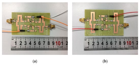
Figure 7.
Photograph of (a) traditional matching BDLNA (bi-directional low noise amplifier) and (b) proposed matching BDLNA.
The curves of |S11| and |S22| for measurement or simulation are shown in Figure 8. Since the input and output matching circuits are topological mirror images, the results for the forward- and reverse-modes are the same. Therefore, only the curves of |S11| and |S22| in the forward mode are given in Figure 8. As can be seen from Figure 8a, the operating band of the proposed BDLNA is broader than that of the traditional one. This is because a flatter port impedance is obtained by using the modified NGD matching circuit for the ON-mode amplifier. After combining the ON- and OFF-mode amplifiers, the operating band is mainly determined by the bandwidth of the ON-mode amplifier when the OFF-mode amplifier has a high port impedance.
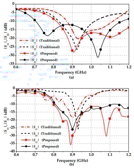
Figure 8.
|S11| and |S22| of the traditional and proposed circuits: (a) simulation and (b) measurement.
The curves of the measured |S11| and |S22| are shown in Figure 8b. There are some negligible differences between the simulation and measurement, which is due to fabrication discrepancies. For the traditional one, the measured bandwidth of return losses greater than 10 dB is 46 MHz from 899 MHz to 945 MHz. For the proposed one, the measured bandwidth is 298 MHz from 797 MHz to 1095 MHz.
The gain and isolation curves are depicted in Figure 9. For the proposed one, although there are some differences between simulated curves and measured curves, the general trend is basically the same. However, the difference between the isolation of the measurement (16.8 dB) and the simulation (23.5 dB) is significant for the traditional BDLNA. The reason for this may be due to the port impedance of the traditional one is not smooth and is greatly affected by the inaccuracy of the fabrication process. In this case, some energy will be returned to the input port through the reverse path as a result of the reduced isolation. For the comparison between the measured curves, the gain of the proposed BDLNA (12.2 dB at 0.915 GHz) is lower than that of the traditional one (14.7 dB). The measured isolation of the proposed BDLNA (24.2 dB) is better than that of the traditional one (16.8 dB). The reason is that the NGD circuit can consume energy by leaking from the reverse path. In this way, the proposed BDLNA can give a better characteristic of isolation.
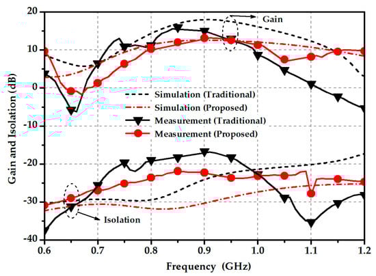
Figure 9.
Simulated and measured gain and isolation.
The value of the stability factor (SF) is shown in Figure 10. The proposed BDLNA is full-band stable (SF > 1) within 0.6 GHz–1.2 GHz, but the traditional BDLNA is not stable within some bands (0.668 GHz–0.784 GHz and 1.105 GHz–1.182 GHz). The reason may be that there is some energy going through the reverse path to the input port. However, even though there was energy feedback in part of the frequency band in the proposed structure, the resistors used in the matching network could consume some feedback energy. Therefore, the stability of the proposed one was better than that of the traditional one.
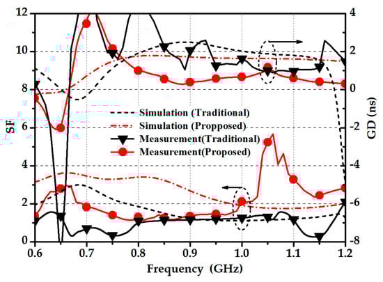
Figure 10.
Simulated and measured SF (stability factor) and GD.
The value of the group delay is described in Figure 10; it was 1.67 ns at 0.915 GHz generated by the traditional BDLNA while it was 0.48 ns for the proposed one. Obviously, the reduction in the group delay was attributed to the use of the NGD circuits. The NDG matching network does not introduce positive delay, it also counteracts the positive delay caused by the FET and the transmission line. Moreover, larger resistances (R1, R2) could decrease GD more, but also generate more losses. Meanwhile, a suitable resistance is needed to transfer the port impendence to be 50 Ω. Therefore, there is a trade-off between the GD and impendence matching performances. In addition, the GD value of the proposed circuit was much flatter compared to that of the traditional one. However, there is a drawback; the resistors used in the NGD matching networks will cause additional noise. Therefore, there also is a trade-off between the GD and noise factor (NF) performances.
The curves of the measured NF are given in Figure 11. For the traditional BDLNA, the value of NF is around 3 dB, but the fluctuation is large near the center frequency of 0.915 GHz. For the proposed BDLNA, the value is about 3.5 dB. The increase in NF was due to the application of resistors in the NGD matching networks. However, the NF curve of the proposed circuit was flatter compared to that of the traditional one. Therefore, the flatness of the NF can also be improved using the NGD circuit.
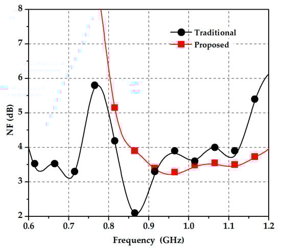
Figure 11.
Measured NF (noise factor) of the traditional and proposed circuit.
The measurement results of these two BDLNAs verified that the proposed NGD circuit could achieve broadband matching. At the same time, higher stability and flatness could also be obtained.
A comparison of the traditional and proposed BDLNAs in this paper with those of previous work is shown in Table 2. The relative bandwidth (RBW) of the proposed BDLNA is broader and the NF was lower than those in References [6,7,23,24,25,26]. For the gain, it was lower than those in References [6,7,22,24] except for those in References [25,26]. This is because only a one-stage FET was adopted in the proposed circuit, but the cascade of the multi-stage transistor was used in those works [6,7,23,24,25,26]. In summary, the NGD circuits with non-Foster characteristics can be used for impedance matching in order to achieve broadband matching.
Table 2.
Performance comparison.
5. Conclusions
In this paper, a switch-less BDLNA with an NGD matching circuit was proposed to realize broadband characteristics. The direction of amplification could be controlled by simply reversing the bias voltages of the FETs. To prove the concept, two amplifiers (a traditional one and the proposed one) were fabricated and measured. For the proposed amplifier, the peak gain was about 12 dB and the noise figure was about 3.5 dB. In addition, the proposed amplifier achieved a broader relative bandwidth (32.6%) compared to the traditional one (5.1%). Additionally, the stability factor is obviously superior to that of the traditional one, and the group delay is much flatter.
Author Contributions
Y.M. and Z.W. contributed to the overall study design, analysis, and writing of the manuscript. S.F., T.S. and H.L. provided technical support and revised the manuscript.
Funding
This work was supported in part by the National Natural Science Foundation of China under Grant 61571075, Grant 61871417, and Grant 51809030, in part by the Youth Science and Technology Star Project Support Program of Dalian City under Grant 2016RQ038, in part by the China Postdoctoral Science Foundation under Grant 2017M611210, and in part by the Fundamental Research Funds for the Central Universities under Grant 3132018185 and Grant 3132016320.
Conflicts of Interest
The authors declare no conflicts of interest.
References
- Kang, D.W.; Kim, J.G.; Min, B.W.; Rebeiz, G.M. Single and Four-Element Ka-Band Transmit/Receive Phased-Array Silicon RFICs with 5-bit Amplitude and Phase Control. IEEE Trans. Microw. Theory Tech. 2009, 57, 3534–3543. [Google Scholar] [CrossRef]
- Weng, S.H.; Chang, H.Y.; Wang, Y.C. A Broadband Bidirectional Amplifier Using Gm-Bandwidth Extension Technique. IEEE Microw. Wirel. Compon. Lett. 2016, 26, 449–451. [Google Scholar] [CrossRef]
- Archer, J.W.; Sevimli, O.; Batchelor, R.A. Bi-Directional Amplifiers for Half-Duplex Transceivers. In Proceedings of the 1999 21th IEEE Gallium Arsenide Integrated Circuit Symposium, Monterey, CA, USA, 17–20 October 1999; pp. 251–254. [Google Scholar]
- Kim, J.; Buckwalter, J.F. A Switchless, Q-Band Bidirectional Transceiver in 0.12-μm SiGe BiCMOS Technology. IEEE J. Solid-State Circuits 2012, 47, 368–380. [Google Scholar] [CrossRef]
- Kumar, T.B.; Ma, K.; Yeo, K.S. A 60-GHz Bi-Directional Variable Gain Amplifier with Microstrip-Line Interconnect in 65 nm CMOS. In Proceedings of the 2016 IEEE International Workshop on Electromagnetics, Nanjing, China, 16–18 May 2016; pp. 1–3. [Google Scholar]
- Wu, P.Y.; Kijsanayotin, T.; Buckwalter, J.F. A 71–86-GHz Switchless Asymmetric Bidirectional Transceiver in a 90-nm SiGe BiCMOS. IEEE Trans. Microw. Theory Tech. 2016, 64, 4262–4273. [Google Scholar] [CrossRef]
- Cho, M.K.; Baek, D.; Kim, J.G. Compact X-band CMOS Bidirectional Gain Amplifier without T/R Switches. Electron. Lett. 2013, 49, 66–68. [Google Scholar] [CrossRef]
- Lo, W.K.; Chan, W.S.; Li, C.W.; Leung, C.K. Self-Phase Equalised Bidirectional Distributed Amplifier. Electron. Lett. 2007, 43, 626–627. [Google Scholar] [CrossRef]
- Mirzaei, H.; Eleftheriades, G.V. A Resonant Printed Monopole Antenna with an Embedded Non-Foster Matching Network. IEEE Trans. Antennas Propag. 2013, 61, 5363–5371. [Google Scholar] [CrossRef]
- Tang, Q.; Xin, H. Stability Analysis of Non-Foster Circuit Using Normalized Determinant Function. IEEE Trans. Microw. Theory Tech. 2017, 65, 3269–3277. [Google Scholar] [CrossRef]
- Mirzaei, H.; Eleftheriades, G.V. Realizing Non-Foster Reactive Elements Using Negative-Group-Delay Networks. IEEE Trans. Microw. Theory Tech. 2013, 61, 4322–4332. [Google Scholar] [CrossRef]
- Shao, T.; Wang, Z.; Fang, S.; Liu, H.; Fu, S. A Compact Transmission-Line Self-Matched Negative Group Delay Microwave Circuit. IEEE Access 2017, 5, 22836–22843. [Google Scholar] [CrossRef]
- Chaudhary, G.; Jeong, Y. Negative Group Delay Phenomenon Analysis Using Finite Unloaded Quality Factor Resonators. Prog. Electromagn. Res. 2016, 156, 55–62. [Google Scholar] [CrossRef]
- Ravelo, B. Innovative Theory on Multiband NGD Topology Based on Feedback-Loop Power Combiner. IEEE Trans. Circuits Syst. II Express Briefs 2016, 63, 738–742. [Google Scholar] [CrossRef]
- Wang, Z.; Cao, Y.; Shao, T.; Fang, S.; Liu, Y. A Negative Group Delay Microwave Circuit Based on Signal Interference Techniques. IEEE Microw. Wirel. Compon. Lett. 2018, 28, 290–292. [Google Scholar] [CrossRef]
- Ravelo, B. Tee Power Divider and Combiner Based Negative Group Delay Topology. Int. J. RF Microw. Comput. Aided Eng. 2018. [Google Scholar] [CrossRef]
- Wan, F.; Li, N.; Ravelo, B.; Ji, Q.; Li, B.; Ge, J. The Design Method of the Active Negative Group Delay Circuits Based on a Microwave Amplifier and an RL-series Network. IEEE Access 2018, 6, 33849–33858. [Google Scholar] [CrossRef]
- Wan, F.; Wang, L.; Ravelo, B. Canonical Transfer Function of Band-pass NGD Circuits. IET Circuits Devices Syst. 2018. [Google Scholar] [CrossRef]
- Ravelo, B. Methodology of Elementary Negative Group Delay Active Topologies Identification. IET Circuit Devices Syst. 2013, 7, 105–113. [Google Scholar] [CrossRef]
- Mirzaei, H.; Eleftheriades, G.V. Arbitrary-Angle Squint-Free Beamforming in Series-Fed Antenna Arrays Using Non-Foster Elements Synthesized by Negative-Group-Delay Networks. IEEE Trans. Antennas Propag. 2015, 63, 1997–2010. [Google Scholar] [CrossRef]
- Zhang, T.; Xu, R.; Wu, C.-T.M. Unconditionally Stable Non-Foster Element Using Active Transversal-Filter-Based Negative Group Delay Circuit. IEEE Microw. Wirel. Compon. Lett. 2017, 27, 921–923. [Google Scholar] [CrossRef]
- Li, X.; Wang, Z.; Fang, S. An Accurate Effective Radius Formula Based on Taguchi Method for Calculating Resonant Frequency of Electrically Thin and Thick Circular Patch Antennas. Microw. Opt. Technol. Lett. 2015, 57, 2567–2572. [Google Scholar] [CrossRef]
- Suh, B.; Kim, D.; Min, B.W. A 7-GHz CMOS Bidirectional Variable Gain Amplifier with Low Gain and Phase Imbalances. IEEE Trans. Circuits Syst. I Regul. Pap. 2018, 65, 2669–2678. [Google Scholar] [CrossRef]
- Kumar, T.B.; Ma, K.; Yeo, K.S. A 60-GHz Coplanar Waveguide- Based Bidirectional LNA in SiGe BiCMOS. IEEE Microw. Wirel. Compon. Lett. 2017, 27, 742–744. [Google Scholar] [CrossRef]
- Meng, F.; Ma, K.; Yeo, K.S.; Xu, S. A Compact 57–67 GHz Bidirectional LNAPA in 65-nm CMOS Technology. IEEE Microw. Wirel. Compon. Lett. 2016, 26, 628–630. [Google Scholar] [CrossRef]
- Archer, J.W.; Batchelor, R.A.; Sevimli, O. Millimetre-wave Bi-directional Amplifiers. In Proceedings of the 1997 Topical Symposium on Millimeter Waves, Kanagawa, Japan, 7–8 July 1997; pp. 19–22. [Google Scholar]
© 2018 by the authors. Licensee MDPI, Basel, Switzerland. This article is an open access article distributed under the terms and conditions of the Creative Commons Attribution (CC BY) license (http://creativecommons.org/licenses/by/4.0/).