Three Topologies of a Non-Isolated High Gain Switched-Inductor Switched-Capacitor Step-Up Cuk Converter for Renewable Energy Applications


Abstract
1. Introduction
- provide a non-isolated negative to positive voltage path with respect to a common ground;
- higher voltage conversion ratios than the classical Cuk and boost converter due to the SL and SC techniques;
- lower voltage stress across the main switch than the classical Cuk and boost converter, therefore, a switch with low voltage rating and low can be used;
- according to the topology, number of diodes, one capacitor, and one or three inductors have been added to the main Cuk converter to perform the SL and SC in order to increase the voltage gain;
- use of a single switch;
- the main advantage of the classical Cuk converter which is having continuous current in the input and output sides due to the input and output inductors have been kept when designing the proposed topologies.
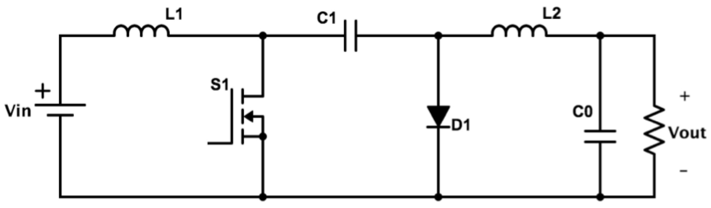
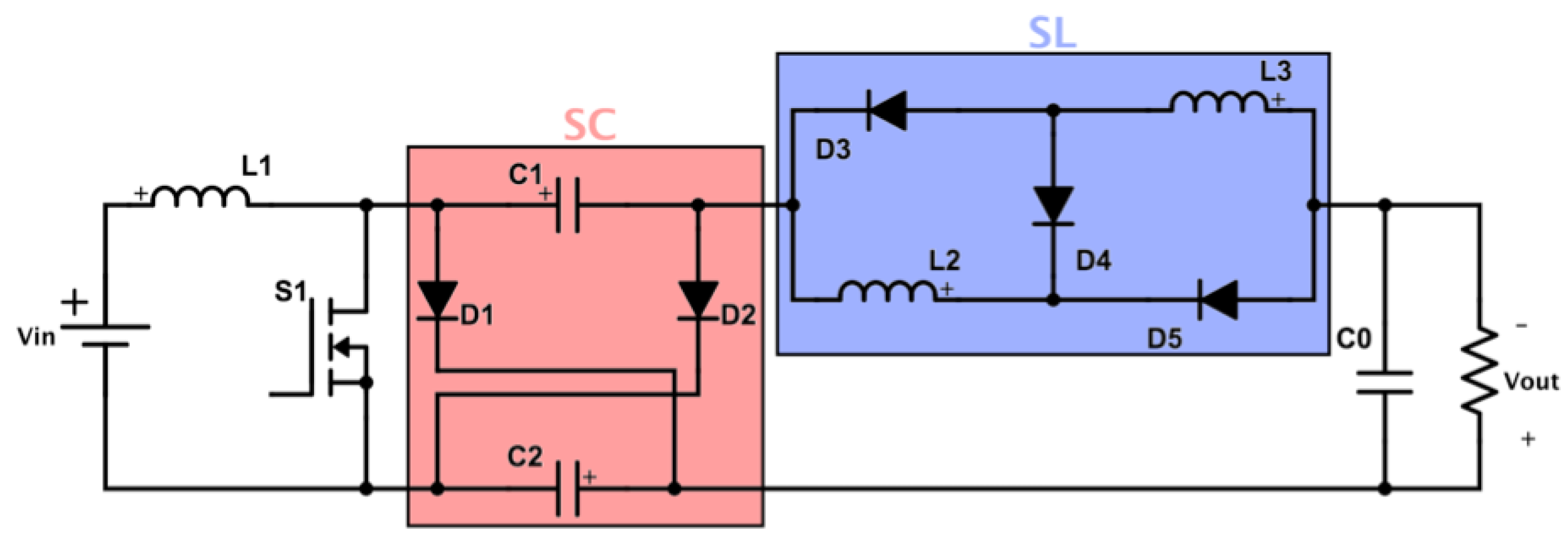
2. Topology-I
2.1. Power Circuit
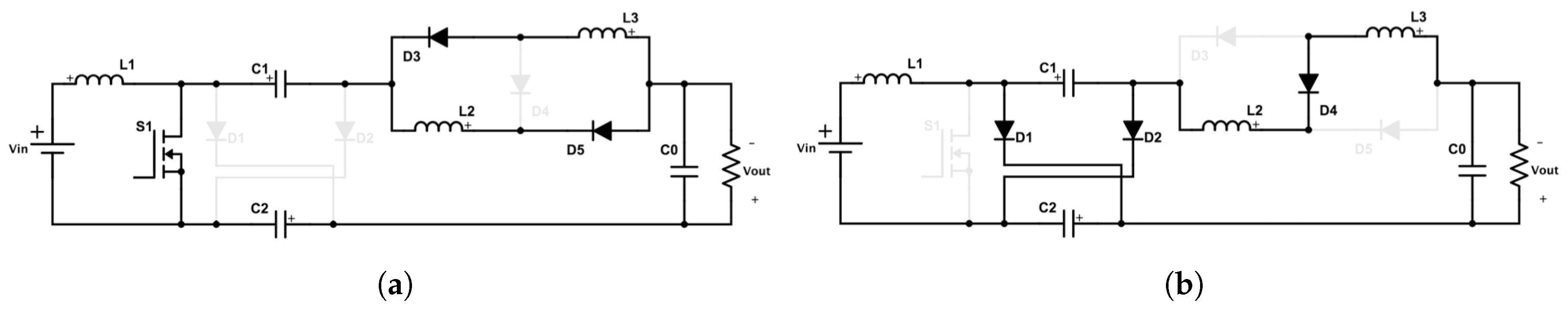
2.2. Modes of Operation
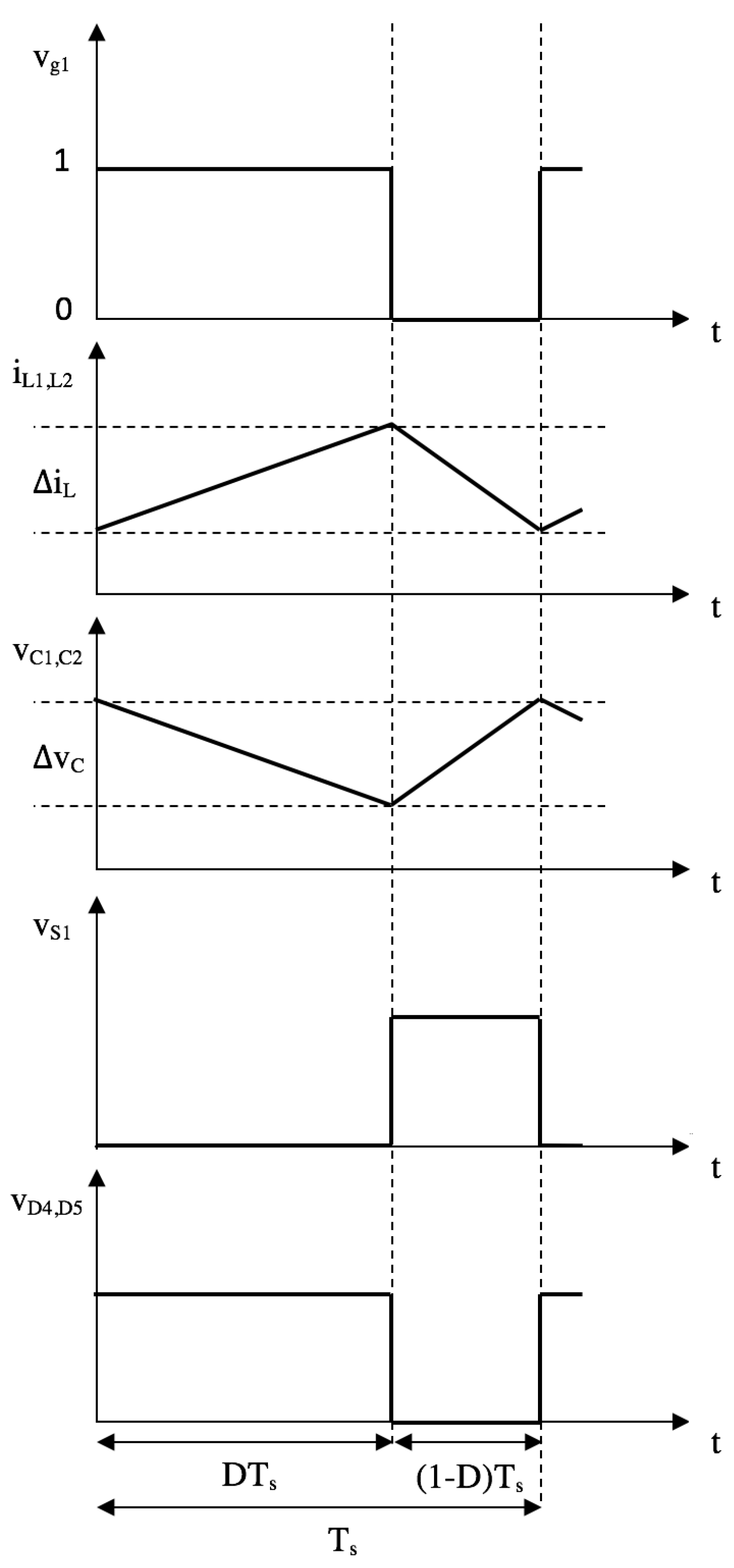
2.2.1. ON-Mode
2.2.2. OFF-Mode
2.3. Circuit Analysis
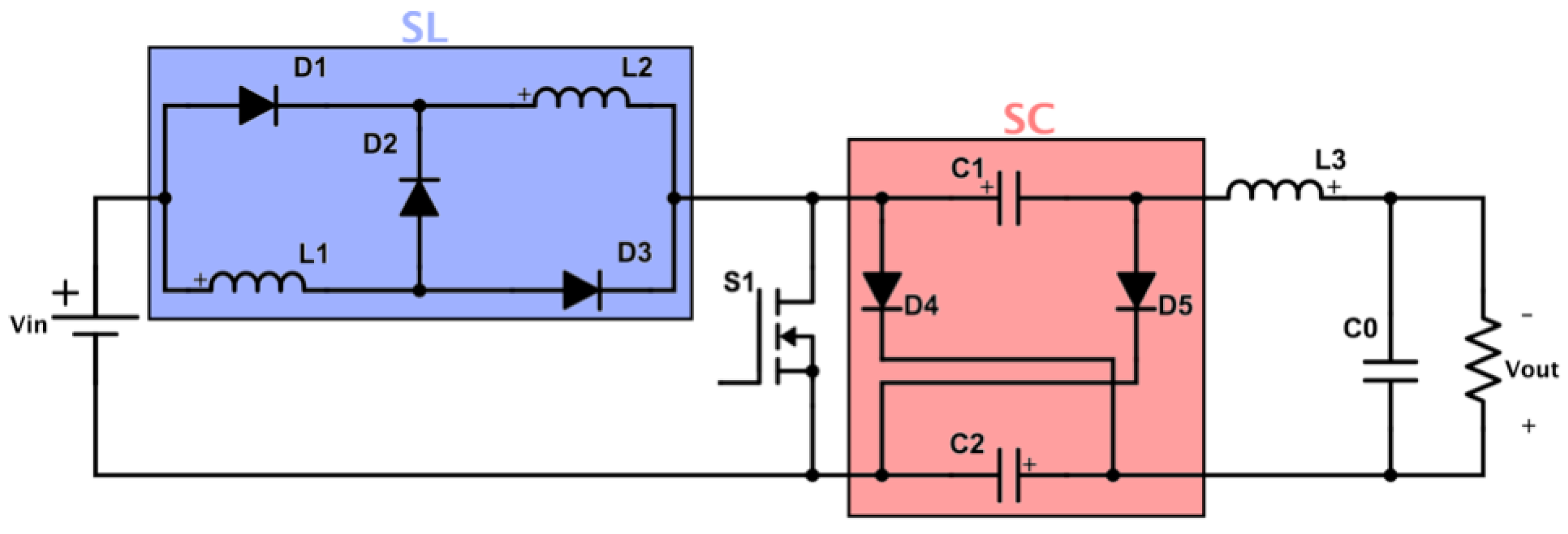
3. Topology-II
3.1. Power Circuit
3.2. Modes of Operation
3.2.1. ON-Mode
3.2.2. OFF-Mode
3.3. Circuit Analysis
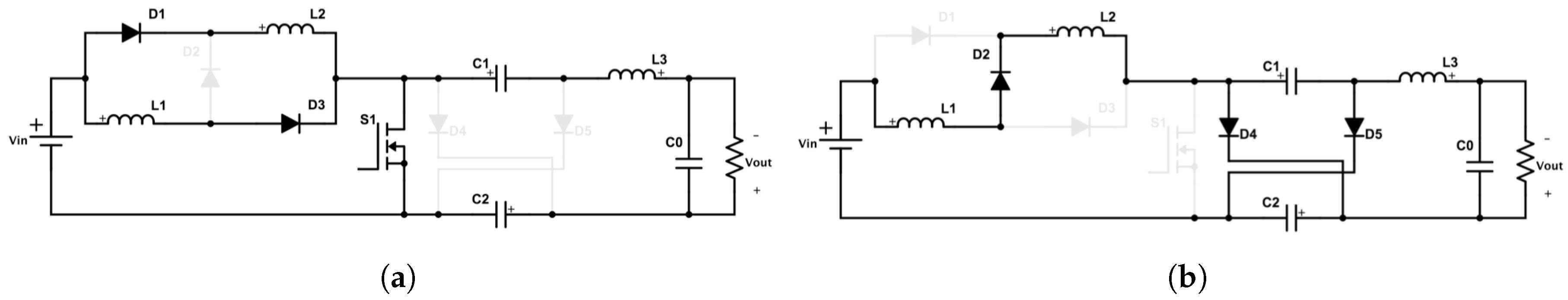
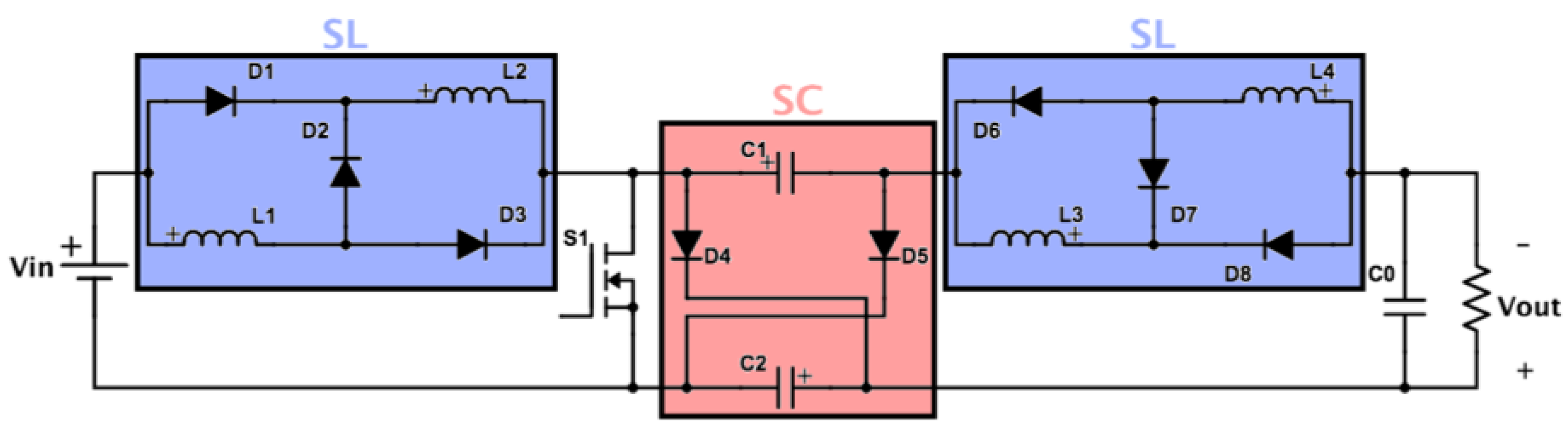
4. Topology-III
4.1. Power Circuit
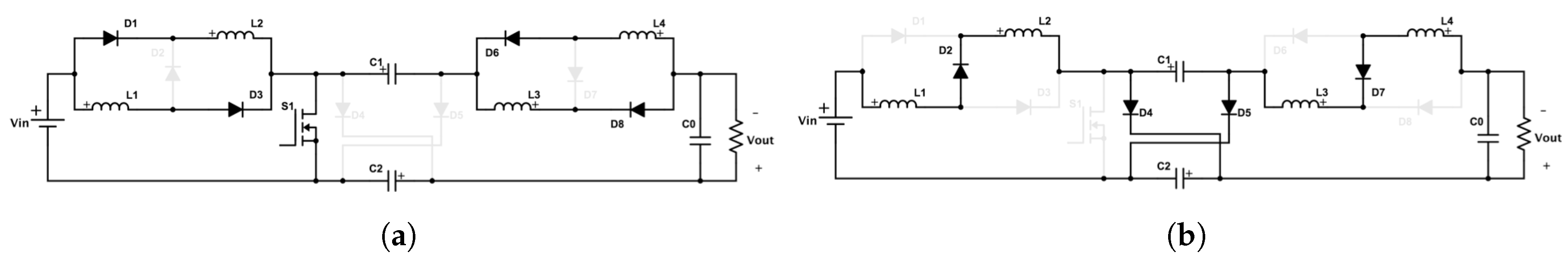
4.2. Modes of Operation
4.2.1. ON-Mode
4.2.2. OFF-Mode
4.3. Circuit Analysis
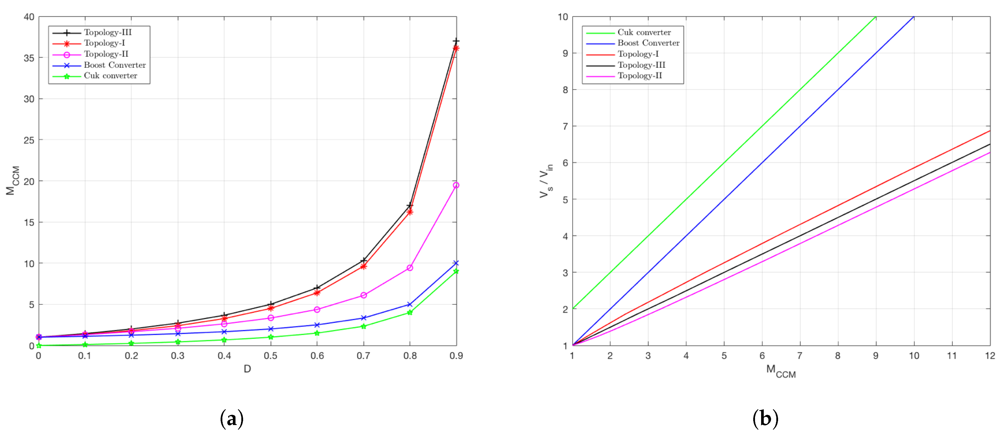
5. Comparison Analysis
6. Results and Discussion
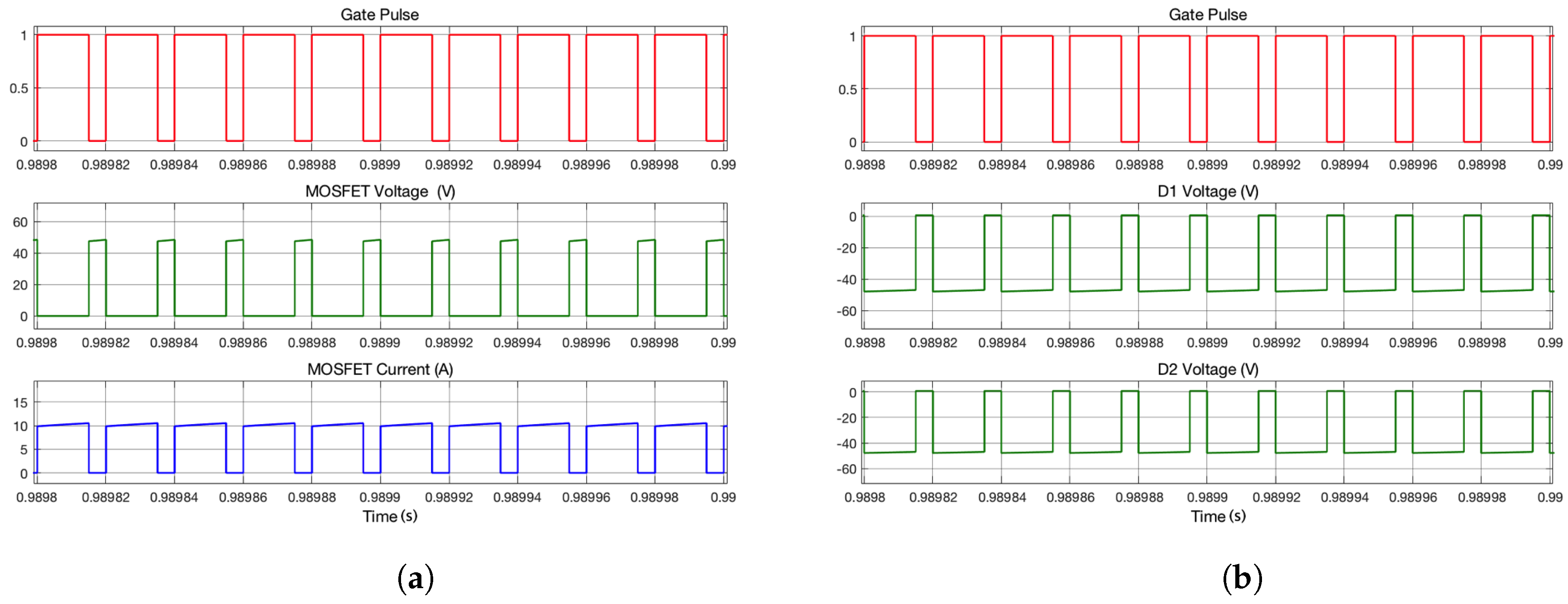
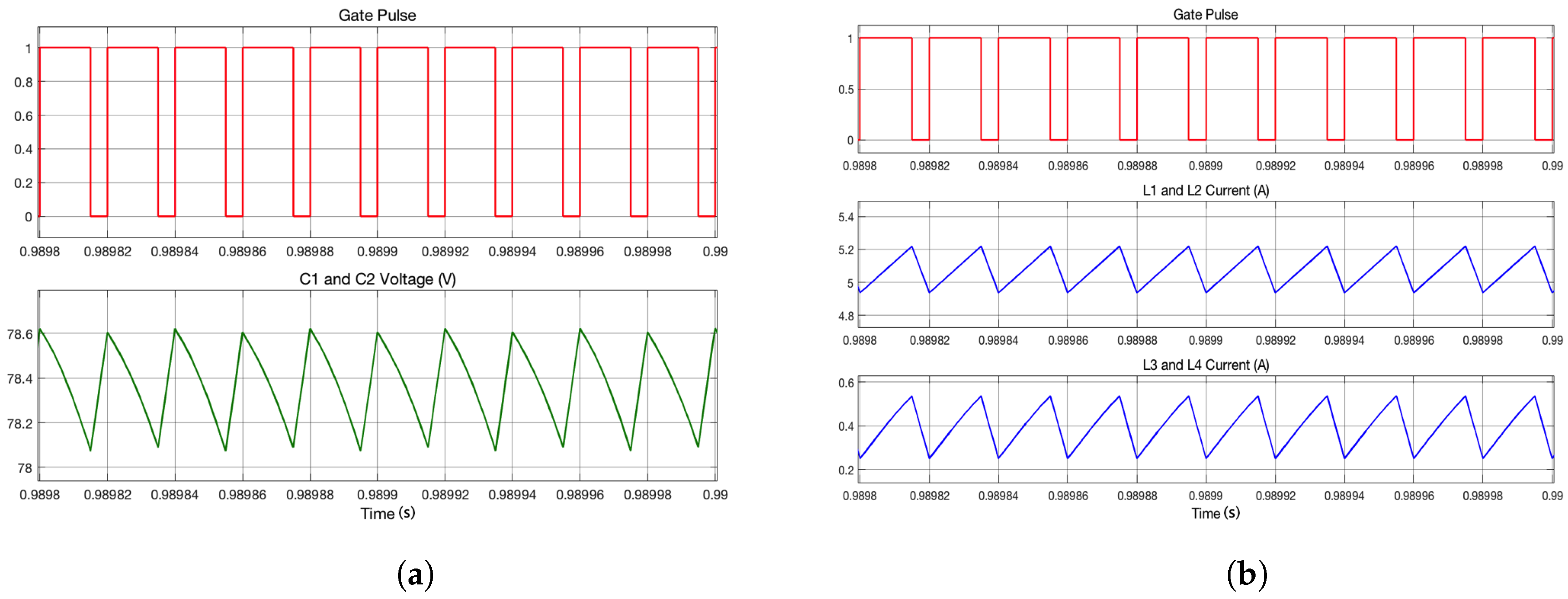
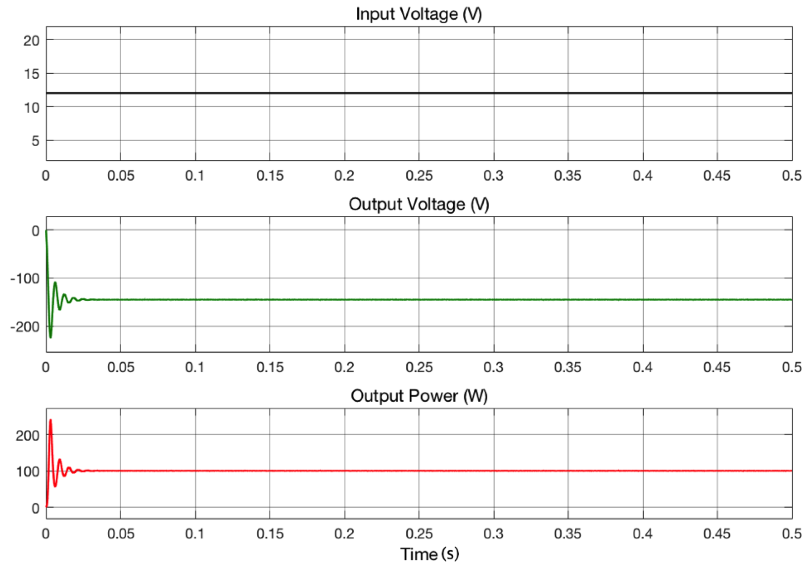
6.1. Topology-I
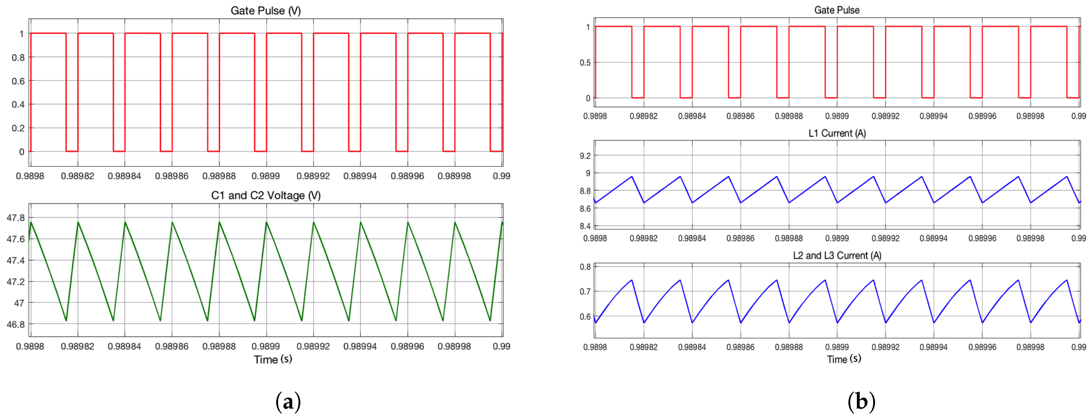
6.2. Topology-II
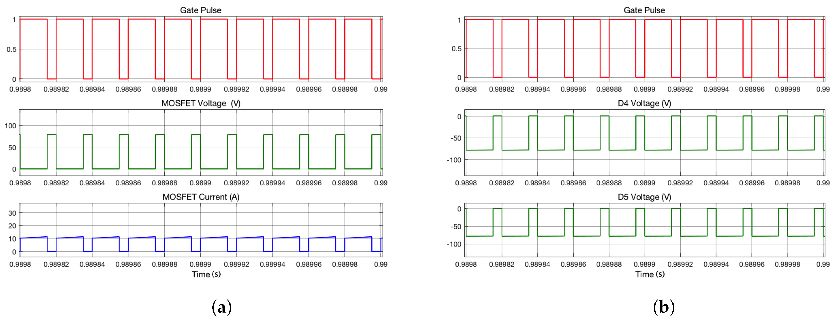
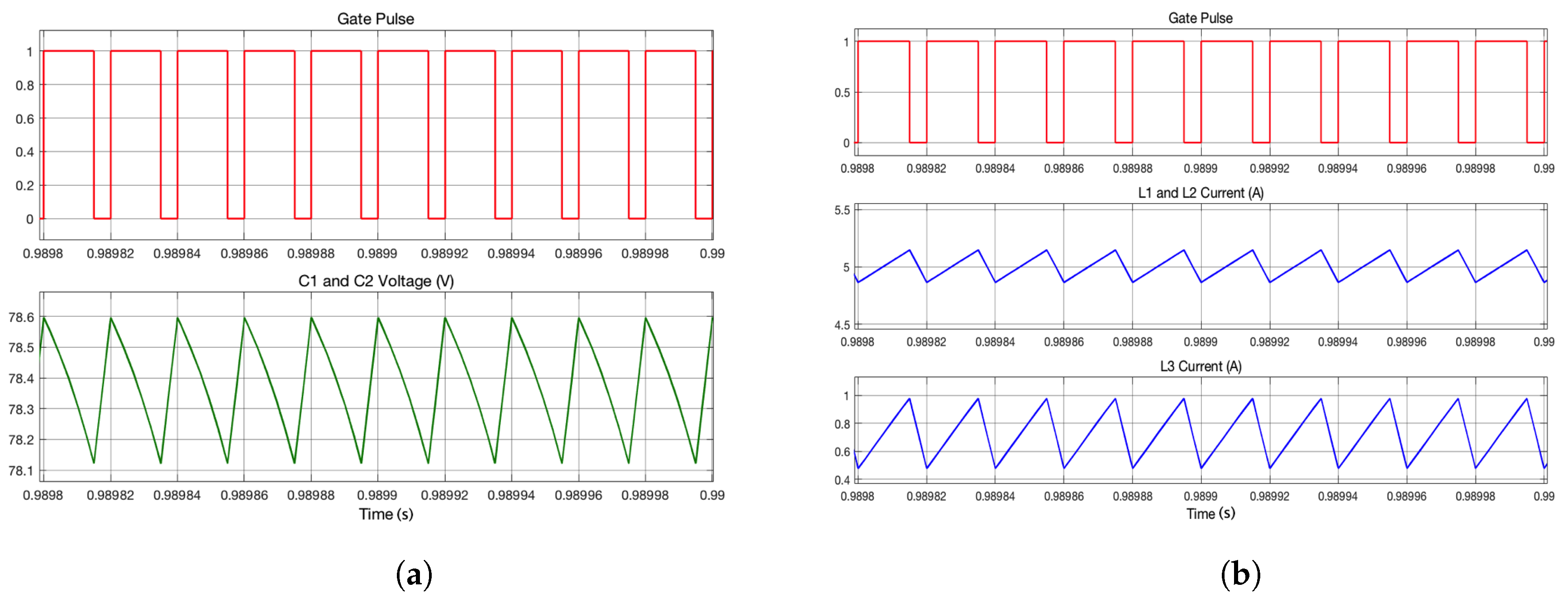
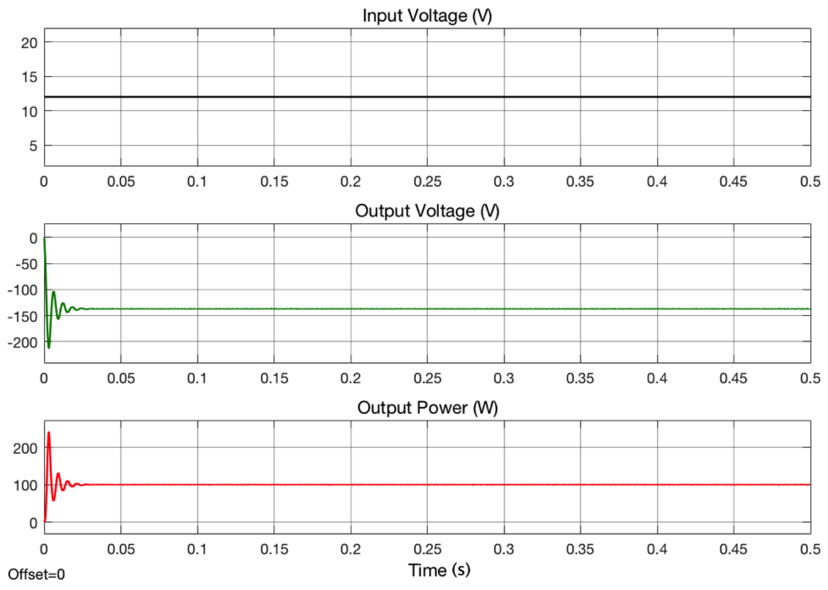
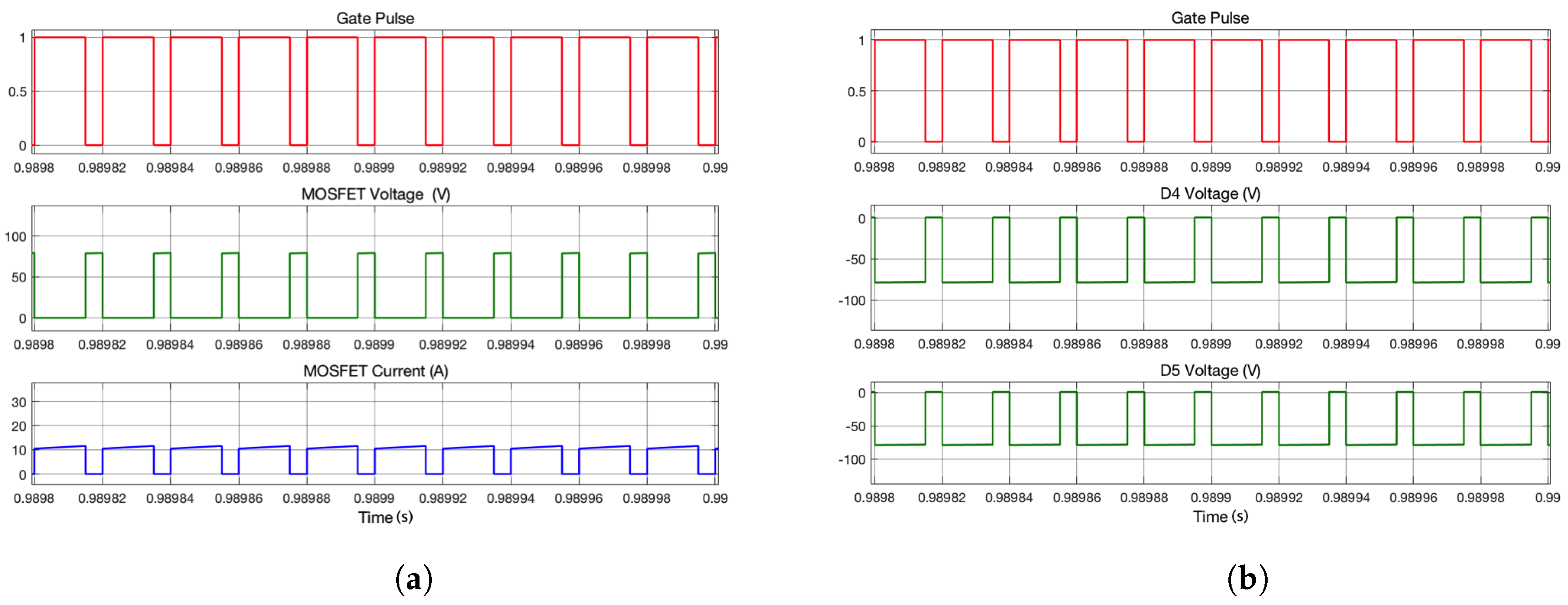
6.3. Topology-III
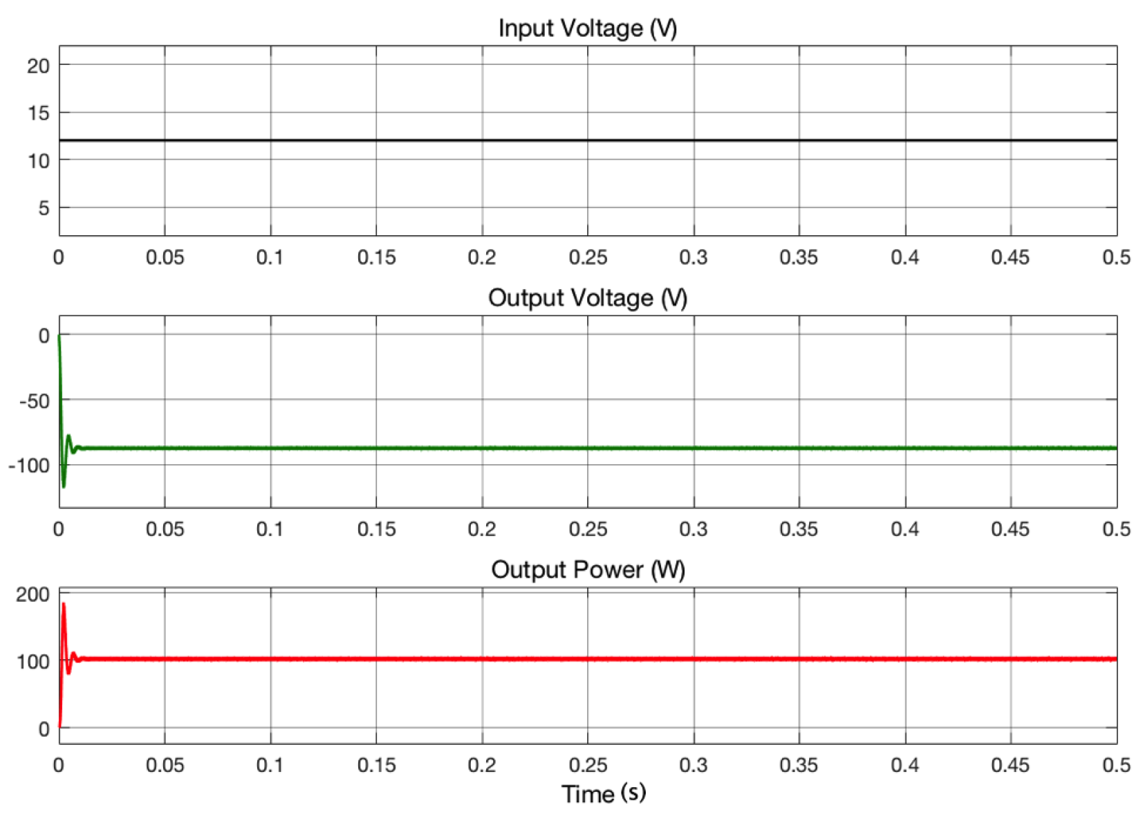
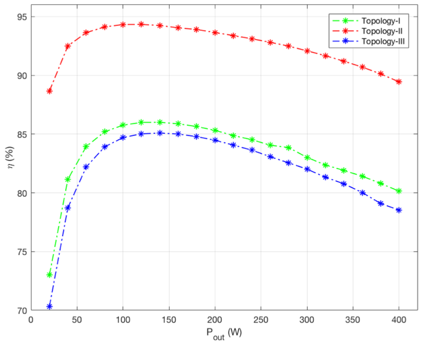
6.4. Efficiency
7. Conclusions
Author Contributions
Conflicts of Interest
References
- Siwakoti, Y.P.; Blaabjerg, F.; Loh, P.C.; Town, G.E. High-voltage boost quasi-Z-source isolated DC/DC converter. IET Power Electron. 2014, 7, 2387–2395. [Google Scholar] [CrossRef]
- Kim, M.; Choi, S. A fully soft-switched single switch isolated dc–dc converter. IEEE Trans. Power Electron. 2015, 30, 4883–4890. [Google Scholar] [CrossRef]
- Zeng, J.; Qiao, W.; Qu, L. LCL-resonant single-switch isolated dc–dc converter. IET Power Electron. 2015, 8, 1209–1216. [Google Scholar] [CrossRef]
- Nguyen, M.; Lim, Y.; Choi, J. Isolated high step-up dc–dc converter based on quasi-switched-boost network. IEEE Trans. Ind. Electron. 2016, 63, 7553–7562. [Google Scholar] [CrossRef]
- Gorji, S.A.; Ektesabi, M.; Zheng, J. Isolated switched-boost push–pull dc–dc converter for step-up applications. Electron. Lett. 2017, 53, 177–179. [Google Scholar] [CrossRef]
- Nguyen, M.; Duong, T.; Lim, Y.; Kim, Y. Isolated boost dc–dc converter with three switches. IEEE Trans. Power Electron. 2018, 33, 1389–1398. [Google Scholar]
- Li, W.; He, X. Review of nonisolated high-step-up DC/DC converters in photovoltaic grid-connected applications. IEEE Trans. Ind. Electron. 2011, 58, 1239–1250. [Google Scholar] [CrossRef]
- de Souza, J.P.; de Oliveira, P.; Gules, R.; Romaneli, E.F.R.; Badin, A.A. A high static gain CUK dc–dc converter. In Proceedings of the 2015 IEEE 13th Brazilian Power Electronics Conference and 1st Southern Power Electronics Conference (COBEP/SPEC), Fortaleza, Brazil, 29 November–2 December 2015; pp. 1–6. [Google Scholar]
- Saravanan, S.; Babu, N.R. A modified high step-up non-isolated dc–dc converter for PV application. J. Appl. Res. Technol. 2017, 15, 242–249. [Google Scholar] [CrossRef]
- Ismail, E.H.; Al-saffar, M.A.; Sabzali, A.J. High conversion ratio dc–dc converters with reduced switch stress. IEEE Trans. Circuits Syst. 2008, 55, 2139–2151. [Google Scholar] [CrossRef]
- Chen, S.M.; Liang, T.J.; Yang, L.S.; Chen, J.F. A cascaded high step-up dc–dc converter with single switch for microsource applications. IEEE Trans. Power Electron. 2011, 26, 1146–1153. [Google Scholar] [CrossRef]
- Hsieh, Y.-P.; Chen, J.-F.; Liang, T.-J.; Yang, L.-S. Novel high step-up dc–dc converter with coupled-inductor and switched-capacitor techniques. IEEE Trans. Ind. Electron. 2012, 59, 998–1007. [Google Scholar] [CrossRef]
- Chien, L.; Chen, C.; Chen, J.; Hsieh, Y. Novel three-port converter with high-voltage gain. IEEE Trans. Power Electron. 2014, 29, 4693–4703. [Google Scholar] [CrossRef]
- Liu, H.; Li, F.; Ai, J. A novel high step-up dual switches converter with coupled inductor and voltage multiplier cell for a renewable energy system. IEEE Trans. Power Electron. 2016, 31, 4974–4983. [Google Scholar] [CrossRef]
- Freitas, A.A.A.; Tofoli, F.L.; Júnior, E.M.S.; Daher, S.; Antunes, F.L.M. High-voltage gain dc–dc boost converter with coupled inductors for photovoltaic systems. IET Power Electron. 2015, 8, 1885–1892. [Google Scholar] [CrossRef]
- Chen, Y.-T.; Lu, Z.-X.; Liang, R.-H. Analysis and design of a novel high-step-up DC/DC converter with coupled inductors. IEEE Trans. Power Electron. 2018, 33, 425–436. [Google Scholar] [CrossRef]
- Muhammad, M.; Armstrong, M.; Elgendy, M.A. Analysis and implementation of high-gain non-isolated DC–DC boost converter. IET Power Electron. 2017, 10, 1241–1249. [Google Scholar] [CrossRef]
- Mostaan, A.; Baghramian, A. Enhanced self lift ZETA converter for negative-to-positive voltage conversion. In Proceedings of the 4th Power Electronics, Drive Systems & Technologies Conference (PEDSTC2013), Tehran, Iran, 13–14 Feburary 2013; pp. 212–217. [Google Scholar]
- Zhu, M.; Luo, F.L. Enhanced self-lift Cûk converter for negative-to-positive voltage conversion. IEEE Trans. Power Electron. 2010, 25, 2227–2233. [Google Scholar] [CrossRef]
- Chen, W.; Liu, Y.; Li, X.; Shi, T.; Xia, C. A novel method of reducing commutation torque ripple for brushless DC motor based on Cuk converter. IEEE Trans. Power Electron. 2017, 32, 5497–5508. [Google Scholar] [CrossRef]
- Ćuk, S.; Middlebrook, R. A general unified approach to modelling switching DC-to-DC converters in discontinuous conduction mode. In Proceedings of the 1977 IEEE Power Electronics Specialists Conference, Palo Alto, CA, USA, 14–16 June 1977; pp. 36–57. [Google Scholar]
- Chincholkar, S.; Chan, C. Design and implementation of an output feedback controller for the Cuk converter. In Proceedings of the IECON 2015—41st Annual Conference of the IEEE Industrial Electronics Society, Yokohama, Japan, 9–12 November 2015; pp. 86–90. [Google Scholar]
- Ismail, E.H.; Al-Saffar, M.A.; Sabzali, A.J.; Fardoun, A.A. A family of single-switch PWM converters with high step-up conversion ratio. IEEE Trans. Circuits Syst. I Regul. Pap. 2008, 55, 1159–1171. [Google Scholar] [CrossRef]
- Axelrod, B.; Berkovich, Y.; Ioinovici, A. Hybrid switched-capacitor-Cuk/Zeta/Sepic converters in step-up mode. In Proceedings of the 2005 IEEE International Symposium on Circuits and Systems, Kobe, Japan, 23–26 May 2005; pp. 1310–1313. [Google Scholar]
- Zhou, D.; Pietkiewicz, A.; Cuk, S. A three-switch high-voltage converter. IEEE Trans. Power Electron. 1999, 14, 177–183. [Google Scholar] [CrossRef]
- Luo, F.L. Seven self-lift dc–dc converters, voltage lift technique. IEE Proc. Electr. Power Appl. 2001, 148, 329–338. [Google Scholar] [CrossRef]
- Axelrod, B.; Berkovich, Y.; Ioinovici, A. Switched-capacitor/switched-inductor structures for getting transformerless hybrid dc–dc PWM converters. IEEE Trans. Circuits Syst. I Regul. Pap. 2008, 55, 687–696. [Google Scholar] [CrossRef]
- Tang, Y.; Fu, D.; Wang, T.; Xu, Z. Hybrid switched-inductor converters for high step-up conversion. IEEE Trans. Ind. Electron. 2015, 62, 1480–1490. [Google Scholar] [CrossRef]


| Topology | Boost | Cuk | Topology-I | Topology-II | Topology-III |
|---|---|---|---|---|---|
| Active switches | 1 | 1 | 1 | 1 | 1 |
| Diodes | 1 | 1 | 5 | 5 | 8 |
| Inductors | 1 | 2 | 3 | 3 | 4 |
| Capacitors | 1 | 2 | 3 | 3 | 3 |
| Voltage Gain |
| Parameter | Value | Unit |
|---|---|---|
| Input voltage () | 12 | V |
| Output voltages () | −137/−87/−145 | V |
| Rated power () | 100 | W |
| Switching frequency () | 50 | kHz |
| Duty cycle (D) | 75% | - |
| Inductors ( ∼ ) | 600 | H |
| Capacitors ( and ) | 22 | F |
| Load () | 190/75/210 |
| 15 m | 0.7 V | 30 m |
© 2018 by the authors. Licensee MDPI, Basel, Switzerland. This article is an open access article distributed under the terms and conditions of the Creative Commons Attribution (CC BY) license (http://creativecommons.org/licenses/by/4.0/).
Share and Cite
Almalaq, Y.; Matin, M. Three Topologies of a Non-Isolated High Gain Switched-Inductor Switched-Capacitor Step-Up Cuk Converter for Renewable Energy Applications. Electronics 2018, 7, 94. https://doi.org/10.3390/electronics7060094
Almalaq Y, Matin M. Three Topologies of a Non-Isolated High Gain Switched-Inductor Switched-Capacitor Step-Up Cuk Converter for Renewable Energy Applications. Electronics. 2018; 7(6):94. https://doi.org/10.3390/electronics7060094
Chicago/Turabian StyleAlmalaq, Yasser, and Mohammad Matin. 2018. "Three Topologies of a Non-Isolated High Gain Switched-Inductor Switched-Capacitor Step-Up Cuk Converter for Renewable Energy Applications" Electronics 7, no. 6: 94. https://doi.org/10.3390/electronics7060094
APA StyleAlmalaq, Y., & Matin, M. (2018). Three Topologies of a Non-Isolated High Gain Switched-Inductor Switched-Capacitor Step-Up Cuk Converter for Renewable Energy Applications. Electronics, 7(6), 94. https://doi.org/10.3390/electronics7060094