Article

On the Prediction of the Threshold Voltage Degradation in CMOS Technology Due to Bias-Temperature Instability

by
Alejandro Campos-Cruz
,
Guillermo Espinosa-Flores-Verdad
,
Alfonso Torres-Jacome
and
Esteban Tlelo-Cuautle
*,†
Department of Electronics, National Institute of Astrophysics, Optics and Electronics (INAOE), Puebla 72840, Mexico
*
Author to whom correspondence should be addressed.
These authors contributed equally to this work.
Electronics 2018, 7(12), 427; https://doi.org/10.3390/electronics7120427
Submission received: 15 October 2018 / Revised: 7 December 2018 / Accepted: 8 December 2018 / Published: 11 December 2018
(This article belongs to the Section Microelectronics)

Abstract

:
Currently, researchers face new challenges in order to compensate or even reduce the noxious phenomenon known as bias-temperature instability (BTI) that is present in modern metal-oxide-semiconductor (MOS) technologies, which negatively impacts the performance of semiconductor devices. BTI remains a mystery in the way that it evolves in time, as well as the responsible mechanisms for its appearance and the further degradation it produces on MOS devices. The BTI phenomenon is usually associated with an increase of MOS transistor’s threshold voltage; however, this work also addresses BTI as a change in MOSFET’s drain current, transconductance, and the channel’s resistivity. In this way, we detail a physics-based model to get a better insight into the prediction of threshold voltage degradation for aging ranges going from days to years, in 180-nm MOS technology. We highlight that a physics-based BTI model improves accuracy in comparison to lookup table models. Finally, simulation results for the inclusion of such a physics-based BTI model into BSIM3v3 are shown in order to get a better understanding of how BTI impacts the performance of MOS devices.

1. Introduction

The challenges of designing integrated circuits (ICs) are focused on accomplishing high reliability and performance, which are partially associated with minimizing aging effects. In this way, research introduces contributions dealing with the understanding of effects like bias temperature instability (BTI). For instance, charge trapping phenomena are known to be a major reliability concern in modern metal-oxide-semiconductor field-effect transistors (MOSFET), playing a significant role in the aging process through analyzing BTI [1]. Furthermore, the influence of process variation has intensively been studied, but only a few works have analyzed the aging mechanisms to find optimal device sizes in analog circuits to guarantee a target of failure rate in fresh and aged conditions [2]. Recent works have addressed the effects of BTI on the power consumption of MOS circuits [3], and the conclusion is that time-dependent performance degradation of MOS technology is a big challenge to enhance IC design. For such reasons and due to the continuous development of modern MOS technologies, reliability phenomena are more severe with each new device’s size down-scaling, as the case of changing from micro-metric silicon to nano-metric high- κ and metal gate technology [4].
In MOS technology, the degradation phenomena is classified as destructive and non-destructive, BTI and hot-carrier injection (HCI) being non-destructive cases and manifesting themselves as charge carrier tunneling from the inversion channel into the gate’s dielectric, due to the continuous increasing of vertical and horizontal electric fields. Destructive degradation manifests as electromigration and time-dependent dielectric breakdown, destroying the physical and electrical functionality of interconnections and the MOS’s gate insulator [5]. The BTI phenomenon was introduced in the 1960s, and recently, a model has been proposed to evaluate the threshold voltage shift that MOS devices experience under severe stress conditions [6] in an electrical simulation. More research on BTI degradation has been published, from the diffusion of hydrogen species and interface bond breaking [7,8,9], to the newest clues of electron’s trap-assisted tunneling from the metal gate into defects within the gate insulator [10,11], as well as the groundbreaking proposal of permanent and recoverable components, which are able to explain both stress and recovery phases as a single phenomenon [12], and finally, the suggestions about a change from the classical model of reaction-diffusion (RD) to switching oxide traps [13].
From the simulation perspective, there are several options to evaluate BTI with a commercial simulator, like Synopsys® MOSRA®, Mentor Graphics ELDO, Cadence RelXpert®, etc. These simulators extrapolate the MOSFET degradation curves from experimental data to obtain the respective degradation of each device in a circuit; even though these results are an estimation, they should not be taken lightly since this estimation has high accuracy even within different commercial simulation tools [14,15]. In this way, most of the published papers to date associate BTI degradation with a continuous increasing of the device’s threshold voltage according to the bias and temperature conditions of the transistors; for such reason, a challenge is the inclusion of a real BTI model to reflect such a change. In this manner, we detail a physics-based BTI model to include the threshold voltage degradation in an electric model and to obtain I-V curves. Once the simulation has been performed, key elements for analog and digital IC design like the drain current, transconductance, and the channel’s resistivity can be obtained.
The remaining organization of this article is as follows: Section 2 describes the BTI’s physics for both conventional silicon-based and high- κ and metal gate technology. Section 3 provides a brief review of the models commonly used to evaluate BTI. Section 4 shows results for the evaluation of the BTI by using a physics-based model that is included in BSIM3v3, as well as the prediction of BTI effects in an extended time range. Finally, the conclusions are listed in Section 5.

2. Bias-Temperature Instability

BTI is commonly associated with an increase of MOSFET devices’ threshold voltage ( V t h ), which leads to charge carrier’s mobility reduction within the conduction channel, ultimately reducing drain current and the transistor’s transconductance. Even though this phenomenon has been known for almost fifty years, its complete understanding remains a mystery. Nevertheless, BTI degradation mechanisms can be associated with interface traps’ ( N i t ) generation, also known as the P b center, oxide charge ( N o t ), and pre-existent defects within the dielectric layer, or oxygen vacancies ( O v ) [4] occupancy due to charge tunneling from the inversion channel. Due to the continuous increase of V t h , each time, a higher gate-voltage is needed to obtain the prior-to-stress overdrive voltage. In old technologies, e.g., the length (L) of the channel wider than 90 nm, BTI was only considered on p-type MOS (pMOS) transistors because its impact on n-type MOS (nMOS) devices is almost negligible. BTI is known as negative (NBTI) for the case of pMOS transistors and positive (PBTI) for nMOS transistors [7].

2.1. Silicon-Based Technology

BTI’s leading mechanism is trap generation at the interface between the substrate and silicon dioxide, so the natural questions is: What are these interface traps, and how can they affect the functionality of MOSFETs?
When silicon oxidizes, the bonding configuration at the surface will depend on the wafer’s crystallographic orientation; while most of the silicon atoms bond to an oxygen atom, some others might bond to hydrogen atoms (the element used for the passivation of point defects during the manufacturing process). An interface trap, also known as the P b center, consists of a silicon atom at Si/SiO 2 interface that has only three complete bonds and an unsatisfied fourth bond, known as a dangling bond. That unoccupied bond is perpendicular to the interface and points towards an oxygen vacancy located above itself [7]. These interface traps are the result of the mismatch between Si/SiO 2 at the interface due to the generated stress during the gate insulator’s thermal growth; these interface traps are capable of trapping charge carriers from the conduction channel. Interface traps are electrically-charged defects throughout the band-gap of silicon acting as generation/recombination centers contributing to leakage currents’ increase and, further, charge carriers’ mobility reduction. While in the upper half of silicon’s band-gap, interface traps are the acceptor-like type, below the mid-gap, they behave as donor-like. Acceptor-like defects placed above the intrinsic Fermi level (E i ) and below the conduction-band level (E C ) have a neutral charge, as well as donor-like defects below the intrinsic level and above the valence-band level (E V ), for the case of intrinsic semiconductor materials.
On pMOS, where the bulk is doped with donor-type impurities, the Fermi level gets closer to the conduction band, so those energy-states between the intrinsic and Fermi levels become negatively charged. When the gate-voltage of a MOSFET device is strong enough to surpass the flat-band condition, the bulk’s energy-bands will slightly bend upwards. When the strong inversion condition is achieved, the intrinsic level will bend below the Fermi level, and the originally negatively-charged states will become neutral again. By the time the device is taken to deep inversion, the intrinsic level will bend above E F , so states between E i and E F will become positively charged, meaning that bonds at the interface have broken. For the case of nMOS devices, in which the substrate is acceptor-type doped, the interface trap’s generation is the inverse process, considering that the bias condition for an nMOS is positive at the gate electrode, so the energy bands will bend downwards, and those states placed between Fermi and intrinsic level will become negatively charged, trapping electrons instead of holes [7].
A second BTI mechanism is oxide charge defects, which are charged impurities deposited into the gate oxide during the manufacturing process, K + and/or Na + ions. Nitrogen atoms are commonly used to passivate defects within the gate insulator; one drawback is that nitrogen creates nitrogen-rich layers within the gate insulator, becoming temporary charge traps during stress [7]. The last subtype of oxide charges comprises those stress-generated defects in the gate’s dielectric. All oxide charges have less impact than interface traps. However, depending on oxide charges’ location, the vertical electric field can be modified, further increasing the threshold voltage shift.
BTI is commonly modeled by using the previously-explained mechanisms for silicon technology, comprehended as the n- or p-doped silicon substrate, silicon dioxide as the gate insulator, and polysilicon as the gate electrode. As shown in Figure 1 [7], PBTI is ignored on micro-metric technologies due to its minimal impact in nMOS devices, if compared to pMOS NBTI. Besides, in modern nanometer technologies based on high- κ gate oxides and metal alloys as the gate electrode, PBTI takes a new degradation level, surpassing the overall threshold voltage degradation in pMOS transistors.

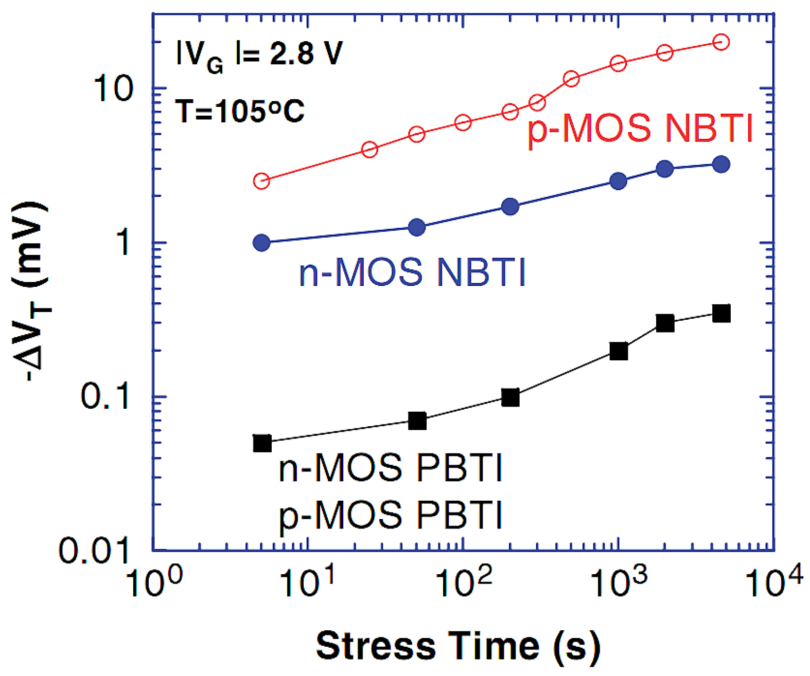
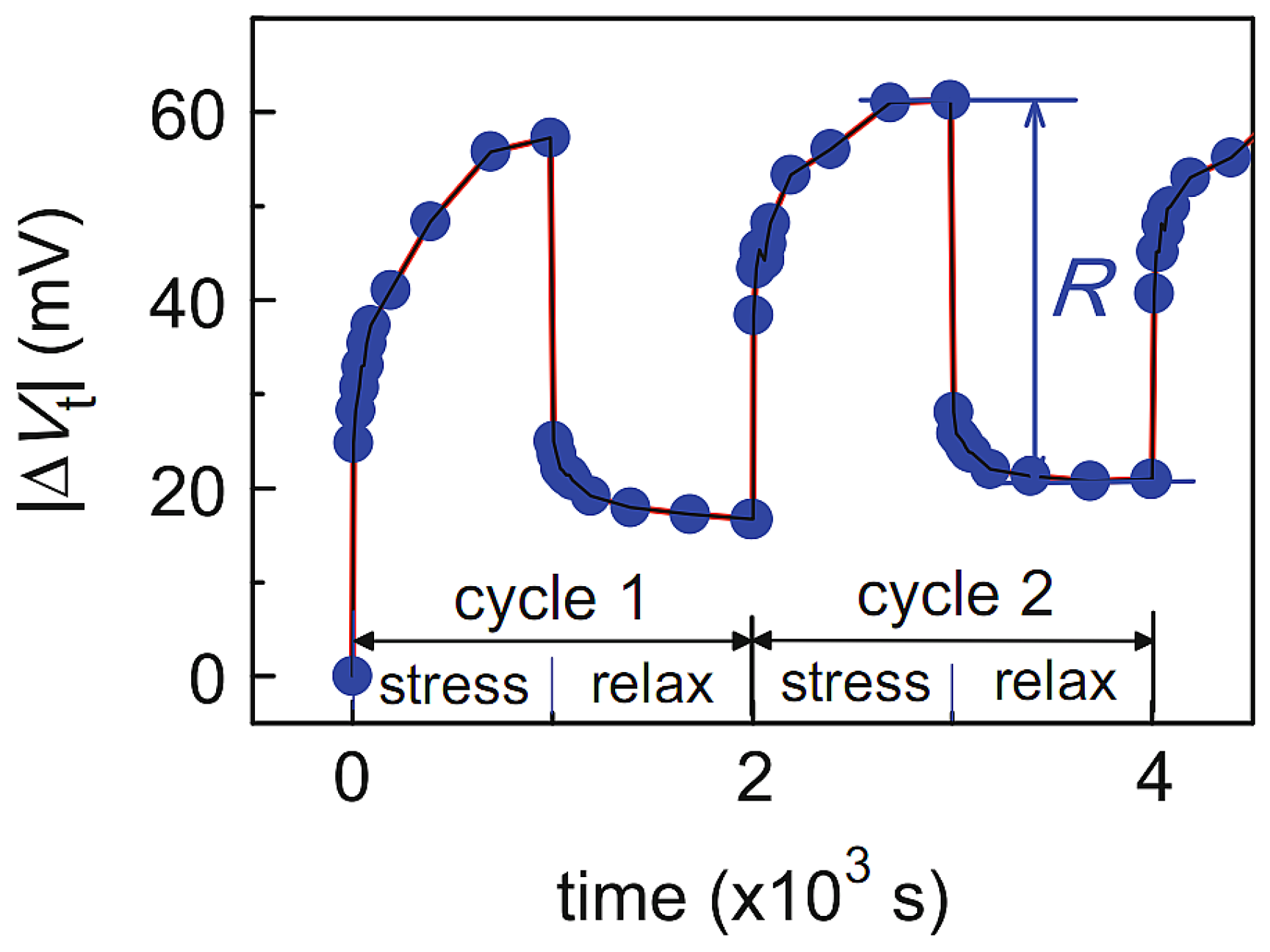
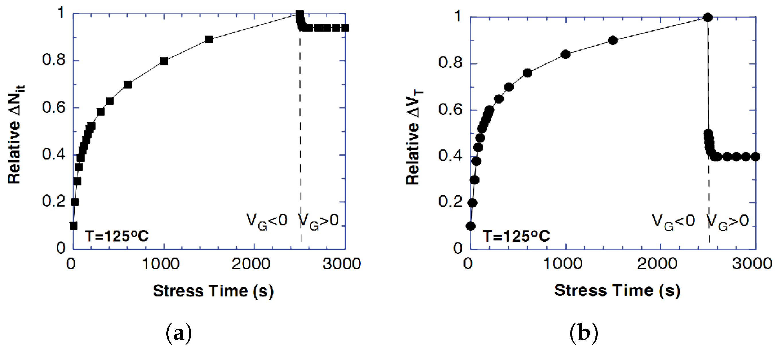
2.2. NBTI and PBTI in CMOS Technology
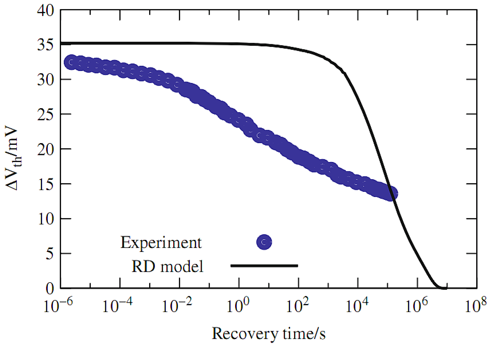
In any MOSFET, both NBTI and PBTI are present at the same time. However, the impact that each degradation phenomenon has on one or another transistor is different, as shown in Figure 1. For this reason, it is common for one degradation component to be ignored due to its minimum impact. In fully-silicon-based technology, it is appreciated that NBTI in both n- and p-type transistors is the main instability source because such an impact is almost one order of magnitude higher on pMOS than it is on nMOS. The reason for NBTI’s impact difference in both pMOS and nMOS transistors is attributed to the lower energy required to dissociate boron-hydrogen bonds within a p-type substrate than the required energy to dissociate phosphorus-hydrogen bonds in n-type substrates, under the same negative gate voltage. Thereby, the difference on the threshold voltage impact is associated with the difficulty in breaking B-H and P-H bonds on the substrate [7].
High- κ and metal gate technology (HKMG) has an advantage over the silicon-based one, keeping the scaling down tendency of the electric inversion layer ( T i n v ), maintaining short-channel effects at the check, and reducing leakage currents. However, as in silicon-based technology, the complete understanding of BTI degradation mechanisms, as well as their respective locations within the gate stack remains unknown. Nevertheless, researchers agree that the possible mechanisms behind BTI’s appearance are: (1) the generation of interface states between the interfacial layer and substrate ( N i t , i l ) and between the interfacial layer and high- κ gate dielectric ( N i t , h k ), (2) the continuous trapping and detrapping of holes/electrons into preexisting oxygen vacancies on either the high- κ layer (HK) or interface layer (IL), and (3) defect generation within the dielectric layer during stress ( N o t ).
NBTI is still being attributed to interface state generation on both Si-substrate/IL and IL/HK interfaces, the Si/IL interface being the one that dominates degradation in pMOS devices. Oxide charges’ contribution becomes negligible, while hole trapping due to oxygen vacancies on the interfacial layer becomes the new degradation mechanisms to take into account ([8,9], and [4], Chapter 21). In the case of PBTI, its new contribution is electron trapping within oxygen vacancies in the high- κ oxide, as well as trap generation in the high- κ dielectric’s bulk during the stress phase. Interface traps’ generation remains the dominant component, as well as in NBTI ([11,16], and [4], Chapters 21 and 22).
BTI is then a phenomenon taking place while MOS devices are turned on, so the high gate voltage and elevated operation temperature are just acceleration factors. A second stage of this phenomenon is present by the time the electrical stress is removed from the device’s gate electrode, known as the recovery phase because the shift in the threshold voltage is reduced to a nearly prior-to-stress value; such a recovery phenomenon is sketched in Figure 2. This BTI’s recovery phase leads to modeling changes, so that the need for an accurate model is evident. Therefore, the best explanation for the BTI phenomenon was provided in [12], where NBTI was modeled as a combination of two uncorrelated components, taking place at different times while in the stress phase. For short stress times ( t s < 10 s), degradation is ruled by a recoverable component ( D R ), while for longer stress times, the permanent component ( D P ) dominates. That way, the recovery phase can be described as the coexistence between a recoverable and a permanent component, in which their dynamics will only be influenced by the gate stack’s manufacturing nature.

3. BTI Models

By 1977, the reaction-diffusion (RD) model [6] was more than enough to fit the measured BTI data with an analytical equation in a simulator and to be able to predict the BTI behavior, even though the discovery of the recovery phase showed the need for model changing due to the incapability of the RD model to predict BTI correctly under AC stress, as shown in Figure 3.
BTI has been under several changes in order to unify both the degradation and recovery phase into one set of mathematical equations; the non-dispersive reaction-diffusion, reaction-dispersion-diffusion (RDD), and switching traps models [13,17] are some examples of the efforts to fit BTI measured data into an equation. An interesting detail is that even though some authors have stated that the RD model is not accurate enough, the RD basics are still the leading mechanisms triggering the aging phenomenon, even on nano-metric and sub-nanometric technology. To understand every BTI model change, key references are [4,7,13,17].
There are two ways to perform aging simulation: the first one is through lookup-table (LUT)-based models, and the second one is with physics-based models. LUT-based models are the most used way to evaluate BTI degradation, not only for a single MOSFET, but in a whole electronic circuit. LUT-based models are easy to use, and the computational cost is low, so they are the logical choice to implement into a commercial simulator like HSPICE®. On the other hand, physic-based models are a more accurate way to evaluate BTI degradation at the expense of larger simulation times even for a single transistor. In this work, we propose the use of a physics-based model for extended time aging simulations.
LUT-based models adjust the threshold voltage of MOS devices according to user pre-defined stress time and operation conditions and have already been implemented in commercial simulator tools like HSPICE®-MOSRA®, or Cadence®-RelXpert. MOSRA® performs the aging simulation in two steps in which the electric stress is calculated and further translated as threshold voltage degradation [14]. At the first step of reliability simulation, known as the pre-stress step, the user selects the most vulnerable device of the circuit, so the operation temperature and stress time will be defined; once the operation conditions are set, the electrical stress of the pre-selected device is obtained. For the next step, the previously-calculated electrical stress is translated into V t h degradation and further extrapolated onto each element in the circuit. At the post-stress step of simulation and once the netlist has been aged, MOSRA® performs .DC, .AC, and .Tran analyses and delivers the circuit’s performance degradation [15]. This aging simulation requires less time and computational cost by sacrificing accuracy, compared to physics-based models. Electrical and analytical models are comprehended as part of physics-based models. Electrical models may reduce the complexity of physics-based models by describing the phenomenon with the use of electronic elements, as demonstrated in [18]. The obtained results are good, and the objective of simulation complexity decrease is obtained at the expense of limited operational frequency.
In a physics-based BTI model, the mechanisms taken into account are interface traps’ generation, charge carriers trapping on either preexistent or stress-generated defects within the oxide layers, and oxide charges. For instance, the threshold voltage change for the RD model is described by (1), which includes stress time and operation temperature, N o x being the positive charge density within the oxide layer, N i t the initial interface traps’ density, K o x the relative constant of the gate dielectric, t o x the oxide thickness, and ϵ 0 the vacuum’s permittivity. Figure 4 shows the simulation results for BTI in 0.25- μ m MOS technology, as presented in [7].
Δ V T H , D C = Δ Q o x + Δ Q i t C o x = q ( Δ N o x + Δ N i t ) K o x ϵ 0 t o x

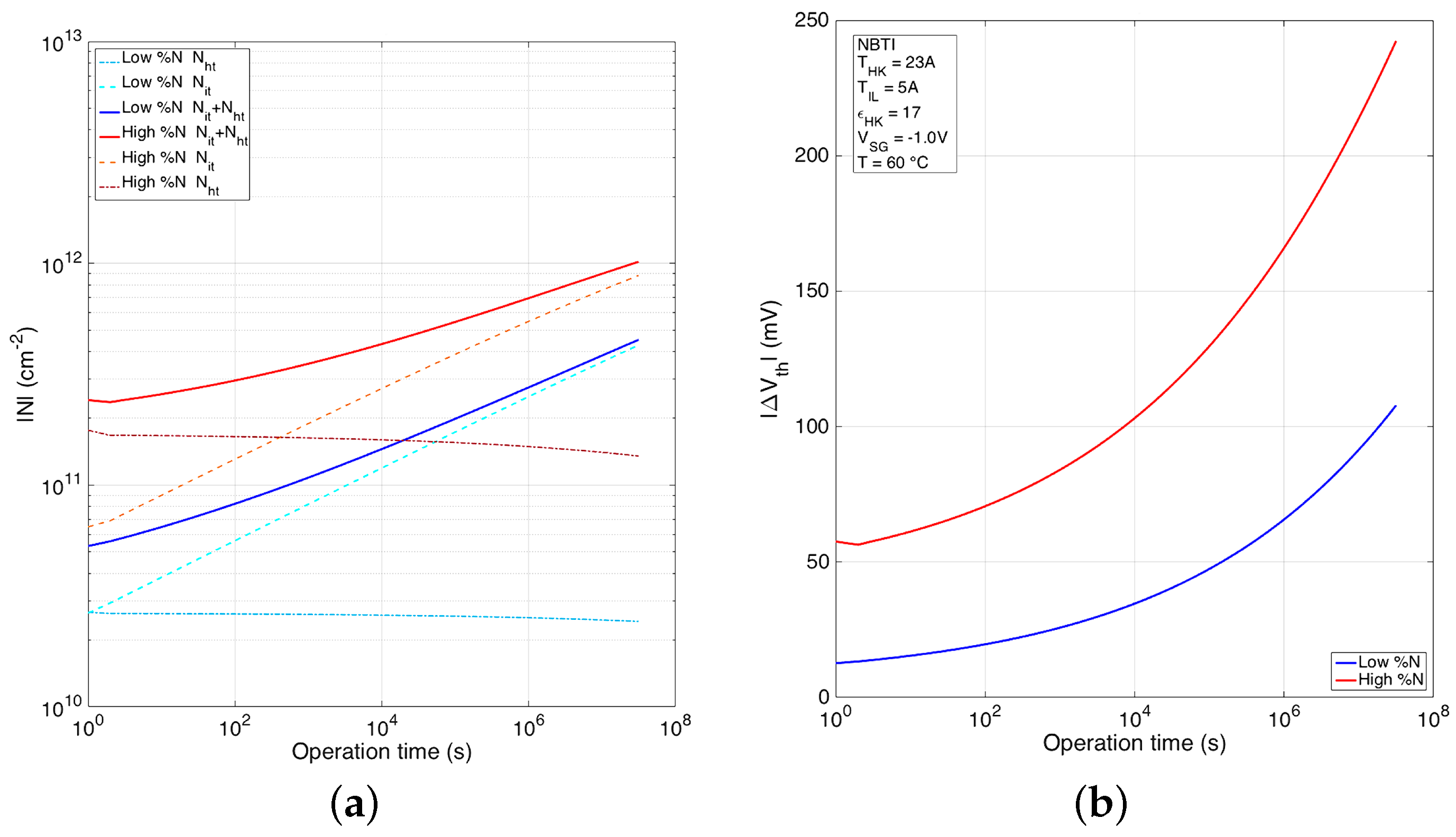
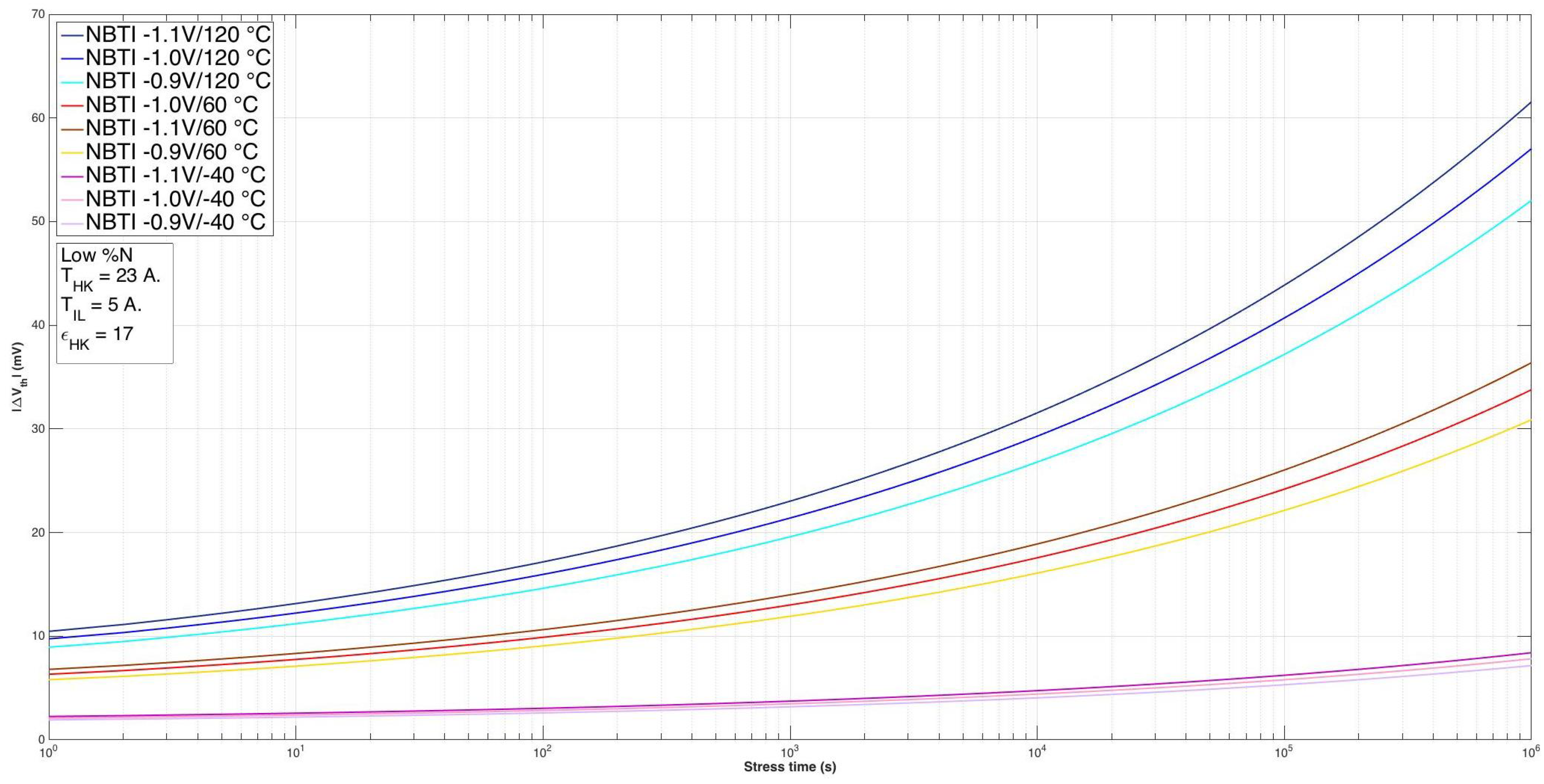
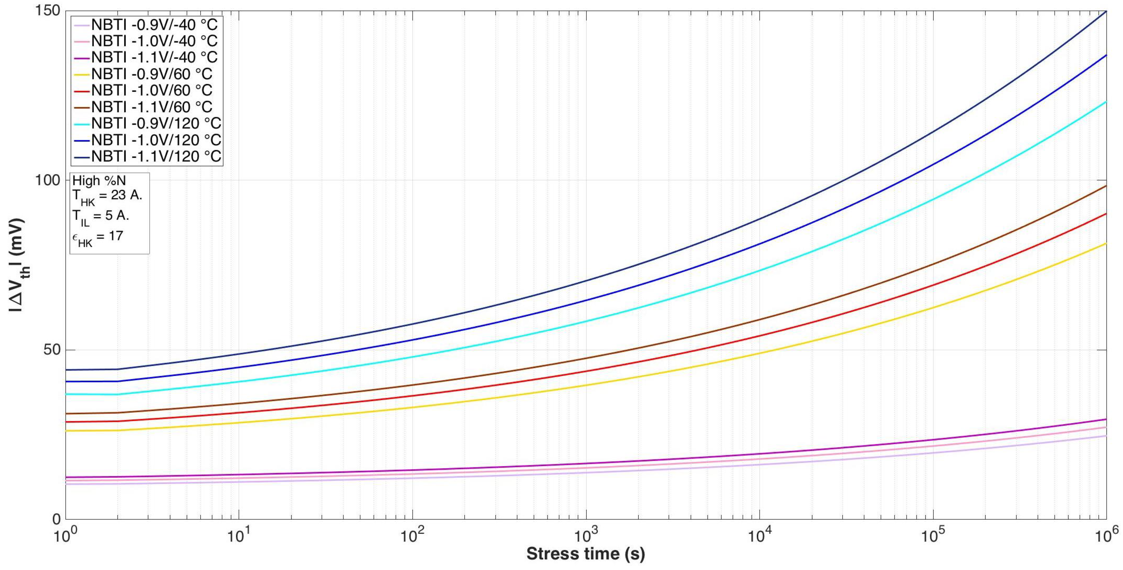
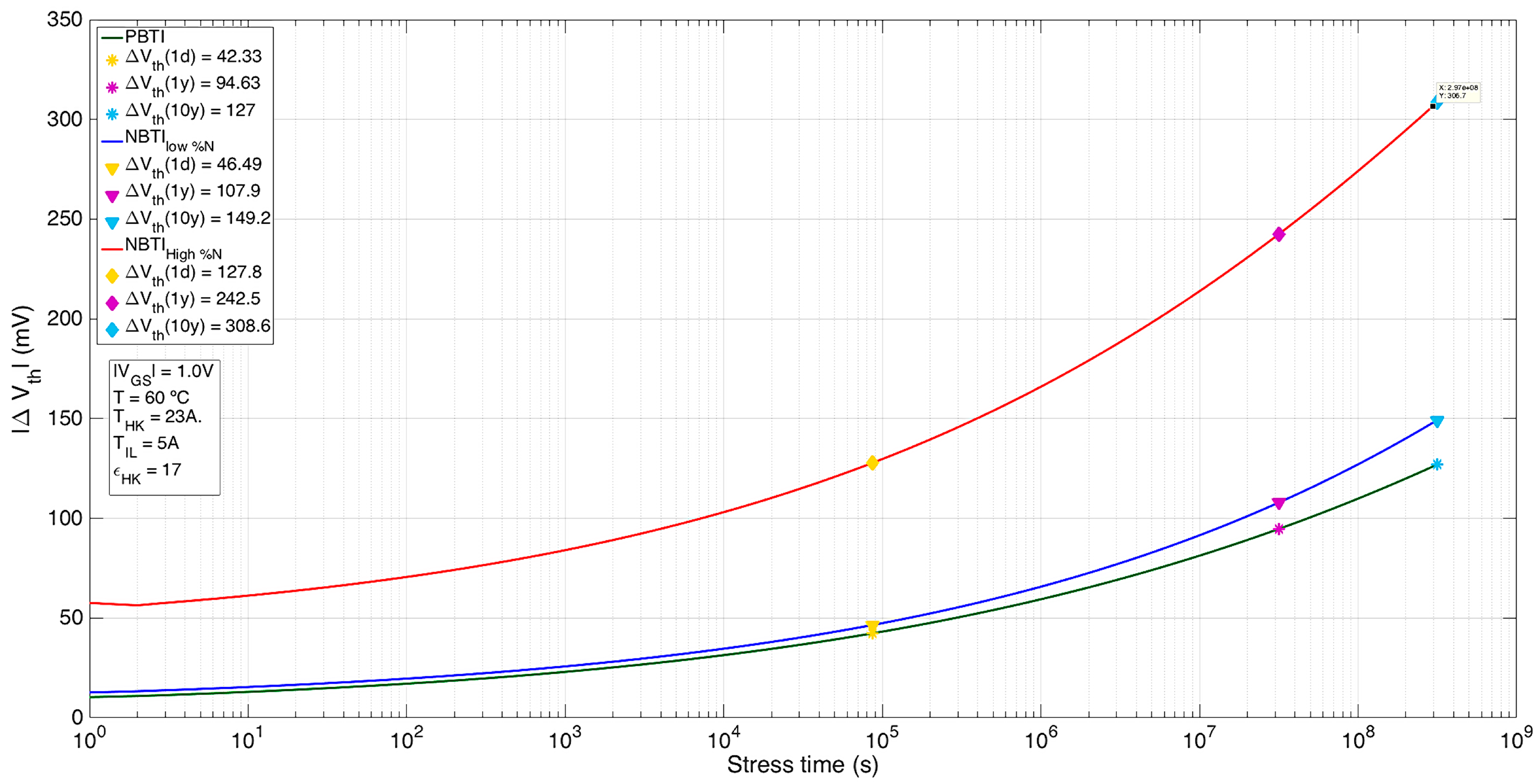
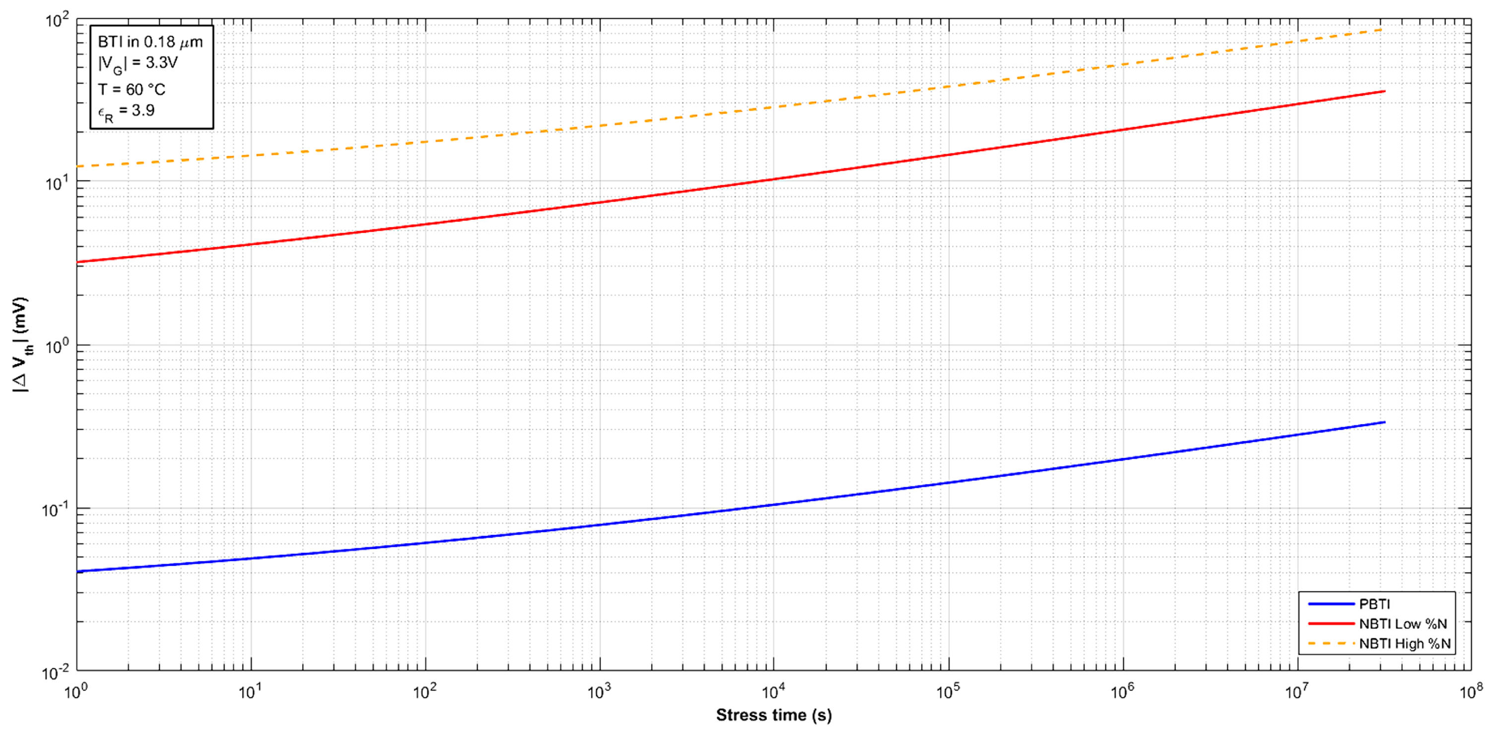
4. BTI Simulation and Discussion of the Results

The physics-based BTI model used herein reflects the impact of the manufacturing process conditions on the performance of MOS devices, and it also shows how degradation can be accelerated under different gate voltage and elevated temperature values during the stress phase. The main advantage of the physics-based model [16,19,20,21] is its capability to evaluate BTI in both fully-silicon-based (Si/SiON) MOSFET technology and high- κ and metal gate nano-metric technology, by adjustment of parameters like the forward and backward-reaction velocity of H/H 2 , the hydrogen diffusion coefficient, and interface traps’ density prior-to-stress at each interface. The model allows both NBTI and PBTI evaluation for different interfacial and high- κ layer thickness, the HK relative dielectric constant, and the nitrogen content within the gate stack. In addition, we show results when including the physics-based BTI model in BSIM3v3 for UMC180-nm MOS technology.

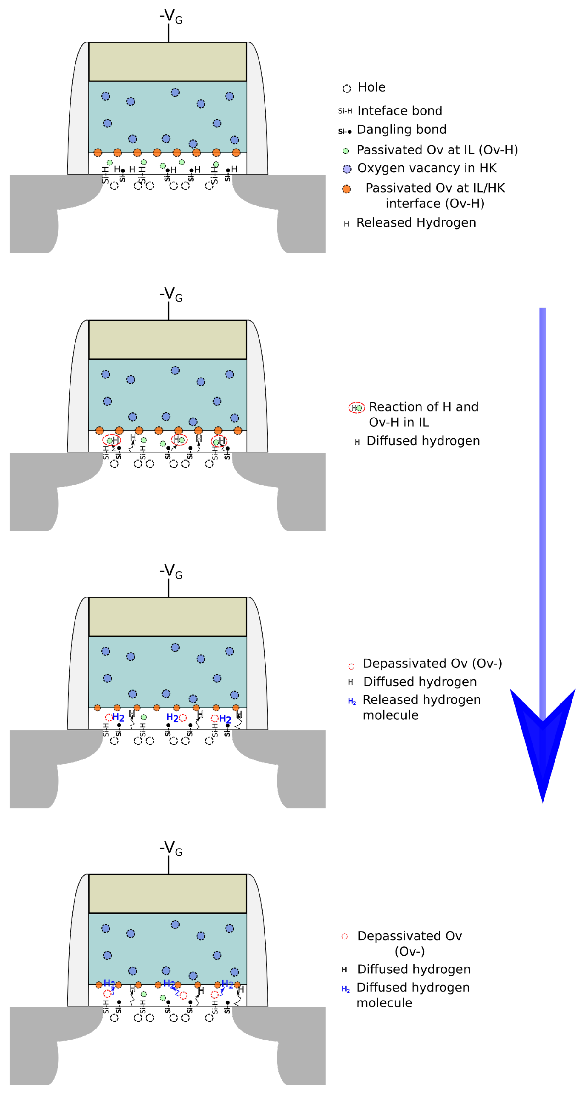
4.1. Physics-Based Model for NBTI

In [19], NBTI degradation was modeled by using three uncorrelated components: (1) interface trap generation at both the substrate and interfacial layer (Si/IL) and the interfacial and high- κ dielectric layer (IL/HK) interfaces, (2) hole trapping into preexistent defects within the interfacial layer, and (3) the generation of new traps within the interfacial layer due to stress. The interface trap component is modeled using the reaction-diffusion model [6], while hole trapping uses the two energy well (2EW) or multi-state model ([4], Chapter 16).
Figure 5 shows the time evolution for NBTI’s interface traps’ generation in accordance with [16,19]. It is described as follows: the holes’ inversion layer at the MOSFET’s conduction channel breaks Si-H bonds located at the Si/IL interface; the released hydrogen atoms diffuse from the interfacial transition layer (SiO x ) and within IL; once at the Si/IL interface, these hydrogen atoms react with more hydrogen atoms breaking Ov-H (oxygen vacancies passivated with hydrogen) bonds. As in the RD model, dangling bonds are created, and H 2 molecules form within the interfacial layer, so at longer stress times, NBTI dynamics will be ruled by the diffusion of H 2 molecules diffusing from the Si/IL to IL/HK interface.
In [20], the differential equations describing interface traps’ generation are presented, as well as the simplified form of those equations is found in [19]. Equation (2) describes the threshold voltage change in nano-metric MOS devices, C o x being the device’s gate capacitance, Δ N I T I L the generation of interface traps, Δ N H T I L the hole trapping related to the degradation process, and Δ N O T I L the bulk trap generation at the Si/IL interface.
Δ V t = q C o x · ( Δ N I T I L + Δ N H T I L + Δ N O T I L )

4.2. Physics-Based Model for PBTI

The simplified model for PBTI degradation on nMOS transistors was provided in [16], including an intensive study of several devices under different manufacturing conditions. Stress-induced leakage currents on nano-metric nMOS transistors have been attributed to oxygen vacancies within the HK dielectric [10,11], which become charge traps for those charge carriers whose energy is close to the conduction-band energy of the high- κ dielectric; that way, the tunneling of electrons from the gate electrode into oxygen vacancies located within the HK dielectric becomes easier. The PBTI’s new affection level is attributed to electron trapping into preexistent traps within HK dielectric layer, as well as trap generation due to electric and thermal stress while the device is under operation.
Just like NBTI, the PBTI model consists of three uncorrelated components: (1) interface traps’ generation at the IL/HK interface, (2) electron trapping into preexistent defects within the HK dielectric layer, and (3) trap generation within the HK dielectric layer during stress. Just like (2), (3) is given for PBTI. Figure 6 shows PBTI dynamics governed by interface traps’ generation in HKMG technology. In such a case, interface trap generation at the interfacial and high- κ dielectric layer interface, as well as activation of passivated oxygen vacancies within the HK dielectric are attributed to Ov-H breaking due to electron tunneling from the inversion channel, within the interfacial dielectric and towards the IL/HK interface. Released hydrogen at the IL/HK interface diffuses, reacts, and breaks passivated defects at the high- κ dielectric and the metal gate electrode (HK/MG) interface. H 2 molecules diffusing from the HK/MG interface is the ruling component for PBTI. PBTI is treated as a newly-discovered degradation phenomenon because almost nothing is known about it.
Δ V t = q C o x · ( Δ N I T H K + Δ N E T H K + Δ N O T H K )
The first logical step before BTI inclusion into the BSIM3v3 model is to verify if the given equations are able to reproduce the measured and reported behavior of the BTI phenomenon over several works. For instance, Figure 7 and Figure 8 show the components that constitute BTI. In both the NBTI and PBTI cases, it can be appreciated that the dominant component is the interface trap generation (see Figure 7a and Figure 8a, respectively), while electron/hole trapping is less by one order of magnitude compared to interface traps. Figure 7b and Figure 8b, respectively, show that charge trapping in preexistent defects has an effect only in early times of stress, while for longer times of stress, the component that dominates is interface trap generation. These results are consistent with reported BTI data in the literature, as well as the fact that defect generation during stress has a negligible impact on the threshold voltage’s change, so it is often ignored in order to reduce the complexity of the evaluation of these simplified equations.
For the NBTI case, it is widely reported that depending on nitrogen content within the gate stack, the overall impact can be higher than PBTI in sub-nanometric nodes. Figure 7b shows the comparison between a device with low and one with high % nitrogen, which is in accordance with measured and reported data on HKGM technology. Low % nitrogen is referred to as ≤0.5 at. %N, and high % nitrogen is considered ≥5 at. %N as defined in [22]. These results prove that both NBTI and PBTI models are good enough to evaluate BTI in both n- and p-type MOSFET transistors. It is important to remark that the simulation time range presented for each result in this work is longer that the ones provided in [5,7,8,9,11,16,19,20,21]. This is one of the contributions presented by this work, verifying the validity of physics-based models for an extended aging range.
Another issue is that nitrogen reduces the BTI permanent component at the expense of the recoverable component increasing, especially during early stress times because such a passivation element creates nitrogen-rich layers within the gate stack that act as temporary charge traps; this increment in the threshold voltage can be seen in Figure 9 and Figure 10. It can be appreciated that at a year of continuous stress, the final degradation value for low nitrogen content has a value slightly higher than 60 mV ( V G = −1.1 V and T = 120 C), while the threshold voltage change for a device with high nitrogen content is 150 mV, nearly 2.5-times greater than low %N. It is interesting to note the trade-off between the impact of recoverable and permanent components in the case of nitrogen addition for defect passivation into the gate stack; this may lead to new research to explore possible alternatives for defect passivation or improving the ALD process.

4.3. BTI Evaluation for Extending Aging Ranges and Inclusion of the BTI Physics-Based Model into BSIM3v3

In the following experiments, nMOS and pMOS devices are biased in the saturation region, as MOS devices usually are for the majority of digital and analog applications. The bias conditions and the sizes are listed in Table 1.
One of the contributions of this work is the evaluation of the physics-based model [16,19] for extended operation times, which up to date has not been reported. Figure 11 shows the simulation result of 10 years of continuous BTI degradation, so markers for one day, one year, and ten years are placed for nMOS PBTI, as well as for NBTI with low and high %N content into the pMOS’s gate stack. In most papers [7,16,19], BTI evaluation results are commonly presented from 1 day–1 week of stress time because, as already explained, the evaluation of such equations is rather difficult, so these results are in fact a great contribution for reliability simulations. On the other hand, obtaining reliability data from field tests is also a difficult task; in order to obtain degradation results for even a week of stress, accelerated degradations conditions must be performed, so the only way to validate the final extrapolated results in Figure 11 is by assuring that short-stress time results are adequate, as is the case of this work.
NBTI and PBTI models can be embedded into BSIM3v3 to evaluate I-V curves. The purpose of such simulation is to obtain “real” information of the measurable effect that BTI can have on MOS devices. The first step is to validate the BSIM3v3 I-V curves for both nMOS and pMOS transistors, as shown in Figure 12 and Figure 13. The second step is hand “adjusting” BTI models to obtain the reported V t h for UMC 0.18- μ m technology, as shown in Figure 14.
The first BTI simulation in the BSIM3v3 I-V model results are shown in Figure 15a,b. The gate voltage was changed from 0 V–3.3 V (for nMOS devices) and from −3.3 V–0 V (for pMOS) with equally-spaced voltage increases of 0.1 V. Due to the increased complexity of evaluating such conditions, the stress time was reduced, presenting only partial results (less than 24 h of continuous stress).
It can be seen that for PBTI (Figure 15a), the threshold voltage shift was less than 0.2 mV, so obtaining drain current reduction is almost impossible. For the NBTI (Figure 15b) case, the V t h shift was 1 mV; due to such a short stress time, these results are still not good. To get better results, new evaluations were performed, in which gate voltages were increased in 1.1-V amounts in order to increase the stress time from one day to one year.
Figure 16 shows that BTI degradation over one year of continuous operation is not so negligible. In Figure 16b, it can be observed that drain current is slowly decreasing with time, especially for higher gate voltages. In this work, the operation conditions are not out of the normal ranges; the gate voltage is the common bias condition for the digital “on” operation ( | V G S | = 3.3 V); and though temperature might be high for one transistor, it is not for an integrated circuit, so it should be kept in mind that BTI degradation can be even further increased. The same analysis was performed on a pMOS device and is shown in Figure 17, in which BTI degradation is more aggressive than it is on nMOS devices.
In Table 2 and Table 3, a list of degraded parameter values (drain current, channel resistance, transconductance, etc.) is presented; the reason for reporting such values is that even though the threshold voltage is a key parameter, IC designers usually work with drain current and the circuit’s transconductance, so these parameters can easily be understood. Reporting these values also helps to understand how BTI degradation affects every electric parameters from a fresh device to a one-year-stressed device under common operation ranges within digital applications, as well as to clarify the real ranges of the BTI degradation of Figure 16 and Figure 17, for which at first, it seems that their threshold voltage change is too pronounced (Figure 16a and Figure 17a), and in their respective current graphs (Figure 16b and Figure 17b), such a change is barely perceptible. The change ranges should be noted; for example in PBTI, such a change is in the order of micro-volt,s which explains why such a curve barely bends, while in the NBTI case, it can be seen that such a change is very perceptible. In this manner, the main contribution of this paper is showing that even though physics-based simulations are more difficult to perform than LUT-based ones, the results are more accurate and can be performed while avoiding getting stuck in the middle of the evaluation, especially at larger operation times.
NBTI high %N is not an easy task on 180-nm technology because there is no data to adjust V t h degradation and getting them into BSIM3v3. Nevertheless, the results of NBTI high %N for one year of BTI degradation are shown next, to highlight the importance of the nitrogen content in the gate insulator. From analyzing Table 2, Table 3 and Table 4, it can be concluded that NBTI is one magnitude of order away from PBTI, proving that PBTI is practically non-existing for silicon-based technology. However, by comparing NBTI high nitrogen content with low nitrogen content, it is clear that high %N is almost double the impact as low %N is, so the drain current can get a variation of 0.34 μ A to nearly 5.9 μ A, which is not good for analog design, where high gains are mandatory.
It is of the highest importance to remark that BTI is not the only degradation phenomenon present in CMOS technology while in the ON operation state; at common bias and temperature conditions, HCI is also present in MOS devices, so TDDB can be considered as the final stage of degradation, leading to charge accumulation within the gate stack and finally destroying the insulating properties of the gate stack. This work only aims to prove the compatibility of a physics-based model within a widely-used electrical model as BSIM3v3 and overcoming the limitations present within the commercial simulators for the reliability evaluation of digital and analog circuits. Most of the published BTI models have been developed for V t h change and have no more impact than that; so the motivation of this work is to take the best possible physics-based model and take it one step further to show that reliability simulation indeed can be enhanced. It has been stated that HCI and BTI appear simultaneously in MOS devices at the given bias and temperature conditions, so it is only natural to question why there is no HCI model included in these simulations? The answer to that question is very simple: BTI and HCI are commonly studied separately because of their complexity, not only at the simulation, but even at the characterization level.
A final comparison step between LUT- and physics-based models is that if the same evaluations are performed in commercial simulators like Synopsys®, MOSRA® or Cadence RelXpert® for the same technology (UMC180 nm) under the same bias and temperature conditions, the results for NBTI will be negligible for even one year of continuous stress under the default BTI reliability parameters, while PBTI evaluation is not even possible on such technology. In order to get measurable results, BTI reliability parameter like interface traps, oxide electric field dependence, and stress time exponent should be adjusted, so unless such parameters are known, the evaluation of BTI degradation might be wrong; as can be seen from the previously-reported results, such BTI degradation on either nMOS or pMOS devices is not inexistent.

5. Conclusions

The physics of the BTI phenomenon has been reviewed for both n- and p-type MOSFET devices. The main effects taking part in the BTI degradation phenomenon have been described, as well as their respective impact on fully-silicon-based technology. Different models for BTI evaluation have been presented, and we showed the simulation of NBTI and PBTI in an extended aging range (up to years), by using physics-based models. In addition, the results for BTI inclusion in the BSIM3v3 I-V model were presented and validated in Figure 16, Figure 17 and Figure 18 and analyzed from the results listed in Table 2, Table 3 and Table 4. Those results demonstrate why PBTI was ignored in fully-silicon-based technology due to its minimum impact on MOS devices’ performance. However, in pMOS devices, such a luxury cannot be allowed. As a result, our contribution highlights the use of a physics-based BTI model in an electric model to measure the overall BTI impact in MOSFET devices for an extended aging range.

Author Contributions

All authors contributed equally to the investigation and writing, review and editing.

Funding

This work was supported in part by INAOE.

Conflicts of Interest

The authors declare no conflict of interest. The founding sponsors had no role in the design of the study; in the collection, analyses, or interpretation of data; in the writing of the manuscript; nor in the decision to publish the results.

References

  1. Both, T.H.; Furtado, G.F.; Wirth, G.I. Modeling and simulation of the charge trapping component of BTI and RTS. Microelectron. Reliab. 2018, 80, 278–283. [Google Scholar] [CrossRef]
  2. Lajmi, R.; Cacho, F.; Larroze, E.L.; Bourdel, S.; Benech, P.; Huard, V.; Federspiel, X. Characterization of Low Drop-Out during ageing and design for yield. Microelectron. Reliab. 2017, 76–77, 92–96. [Google Scholar] [CrossRef]
  3. Halak, B.; Tenentes, V.; Rossi, D. The impact of BTI ageing on the reliability of level shifters in nano-scale CMOS technology. Microelectron. Reliab. 2016, 67, 74–81. [Google Scholar] [CrossRef]
  4. Grasser, T. Bias Temperature Instability for Devices and Circuits; Springer: New York, NY, USA, 2013. [Google Scholar]
  5. Chung, J.E.; Jeng, M.C.; Moon, J.E.; Ko, P.K.; Hu, C. Performance and reliability design issues for deep-submicrometer MOSFETs. IEEE Trans. Electron Devices 1991, 38, 545–554. [Google Scholar] [CrossRef]
  6. Jeppson, K.O.; Svensson, C.M. Negative bias stress of MOS devices at high electric fields and degradation of MNOS devices. J. Appl. Phys. 1977, 48, 2004–2014. [Google Scholar] [CrossRef]
  7. Schroder, D.K. Negative bias temperature instability: What do we understand? Microelectron. Reliab. 2007, 47, 841–852. [Google Scholar] [CrossRef]
  8. Alam, M.A.; Mahapatra, S. A comprehensive model of PMOS NBTI degradation. Microelectron. Reliab. 2005, 45, 71–81. [Google Scholar] [CrossRef]
  9. Mahapatra, S.; Goel, N.; Desai, S.; Gupta, S.; Jose, B.; Mukhopadhyay, S.; Joshi, K.; Jain, A.; Islam, A.; Alam, M. A comparative study of different physics-based NBTI models. IEEE Trans. Electron Devices 2013, 60, 901–916. [Google Scholar] [CrossRef]
  10. Robertson, J.; Xiong, K.; Tse, K.Y. Importance of Oxygen Vacancies in High K Gate Dielectrics. In Proceedings of the IEEE International Conference on Integrated Circuit Design and Technology (ICICDT’07), Austin, TX, USA, 30 May–1 June 2007; pp. 1–4. [Google Scholar]
  11. Cartier, E.; Linder, B.; Narayanan, V.; Paruchuri, V. Fundamental understanding and optimization of PBTI in nFETs with SiO2/HfO2 gate stack. In Proceedings of the International IEEE Electron Devices Meeting (IEDM’06), San Francisco, CA, USA, 11–13 December 2006; pp. 1–4. [Google Scholar]
  12. Huard, V. Two independent components modeling for Negative Bias Temperature Instability. In Proceedings of the 2010 IEEE International Reliability Physics Symposium (IRPS), Anaheim, CA, USA, 2–6 May 2010; pp. 33–42. [Google Scholar] [CrossRef]
  13. Grasser, T.; Kaczer, B.; Goes, W.; Reisinger, H.; Aichinger, T.; Hehenberger, P.; Wagner, P.J.; Schanovsky, F.; Franco, J.; Luque, M.; et al. The Paradigm Shift in Understanding the Bias Temperature Instability: From Reaction-Diffusion to Switching Oxide Traps. IEEE Trans. Electron Devices 2011, 58, 3652–3666. [Google Scholar] [CrossRef]
  14. Tudor, B.; Wang, J.; Chen, Z.; Tan, R.; Liu, W.; Lee, F. An accurate and scalable MOSFET aging model for circuit simulation. In Proceedings of the 2011 12th International Symposium on Quality Electronic Design (ISQED), Santa Clara, CA, USA, 14–16 March 2011; pp. 1–4. [Google Scholar] [CrossRef]
  15. Tudor, B.; Wang, J.; Chen, Z.; Tan, R.; Liu, W.; Lee, F. An accurate MOSFET aging model for 28 nm integrated circuit simulation. Microelectron. Reliab. 2012, 52, 1565–1570. [Google Scholar] [CrossRef]
  16. Mukhopadhyay, S.; Joshi, K.; Chaudhary, V.; Goel, N.; De, S.; Pandey, R.K.; Murali, K.V.R.M.; Mahapatra, S. Trap Generation in IL and HK layers during BTI/TDDB stress in scaled HKMG N and P MOSFETs. In Proceedings of the 2014 IEEE International Reliability Physics Symposium, Waikoloa, HI, USA, 1–5 June 2014; pp. GD.3.1–GD.3.11. [Google Scholar] [CrossRef]
  17. Grasser, T.; Rott, K.; Reisinger, H.; Waltl, M.; Schanovsky, F.; Kaczer, B. NBTI in Nanoscale MOSFETs—The Ultimate Modeling Benchmark. IEEE Trans. Electron Devices 2014, 61, 3586–3593. [Google Scholar] [CrossRef] [Green Version]
  18. Maricau, E.; Zhang, L.; Franco, J.; Roussel, P.; Groeseneken, G.; Gielen, G. A compact NBTI model for accurate analog integrated circuit reliability simulation. In Proceedings of the 2011 European Solid-State Device Research Conference (ESSDERC), Helsinki, Finland, 12–16 September 2011; pp. 147–150. [Google Scholar] [CrossRef]
  19. Joshi, K.; Mukhopadhyay, S.; Goel, N.; Nanware, N.; Mahapatra, S. A Detailed Study of Gate Insulator Process Dependence of NBTI Using a Compact Model. IEEE Trans. Electron Devices 2014, 61, 408–415. [Google Scholar] [CrossRef]
  20. Joshi, K.; Mukhopadhyay, S.; Goel, N.; Mahapatra, S. A consistent physical framework for N and P BTI in HKMG MOSFETs. In Proceedings of the 2012 IEEE International Reliability Physics Symposium (IRPS), Anaheim, CA, USA, 15–19 April 2012; pp. 5A.3.1–5A.3.10. [Google Scholar] [CrossRef]
  21. Joshi, K.; Hung, S.; Mukhopadhyay, S.; Chaudhary, V.; Nanaware, N.; Rajamohnan, B.; Sato, T.; Bevan, M.; Wei, A.; Noori, A.; et al. HKMG process impact on N, P BTI: Role of thermal IL scaling, IL/HK integration and post HK nitridation. In Proceedings of the 2013 IEEE International Reliability Physics Symposium (IRPS), Anaheim, CA, USA, 14–18 April 2013; pp. 4C.2.1–4C.2.10. [Google Scholar] [CrossRef]
  22. Hattangady, S.; Kraft, R.; Grider, D.; Douglas, M.; Brown, G.; Tiner, P.; Kuehne, J.; Nicollian, P.; Pas, M. Ultrathin nitrogen-profile engineered gate dielectric films. In Proceedings of the International IEEE Electron Devices Meeting (IEDM’96), San Francisco, CA, USA, 8–11 December 1996; pp. 495–498. [Google Scholar]
Figure 1. Comparison of NBTI and PBTI in both nMOS and pMOS devices [7].
Electronics 07 00427 g001
Figure 2. Absolute change of the threshold voltage due to electrical stress and further reduction once in the recovery phase ([4], p. 291).
Electronics 07 00427 g002
Figure 3. Recovery phase predictions according to the reaction-diffusion (RD) model and experimental data ([4], p. 382).
Electronics 07 00427 g003
Figure 4. (a) Relative generation of interface traps in the device and (b) the threshold voltage relative change as presented in [7].
Electronics 07 00427 g004
Figure 5. Degradation time evolution for NBTI interface traps’ generation. Ov, oxygen vacancy; IL, interface layer; HK, high- κ layer.
Electronics 07 00427 g005
Figure 6. Degradation time evolution for PBTI interface traps’ generation. MG, metal gate.
Electronics 07 00427 g006
Figure 7. Components that constitute the NBTI phenomenon under different operation conditions. (a) Interface trap generation ( N i t ), hole trapping ( N h t ), and the sum of both N i t and N h t components, and (b) the absolute threshold voltage change.
Electronics 07 00427 g007
Figure 8. Components that constitute the PBTI phenomenon under different operation conditions. (a) Interface trap generation ( N i t ), electron trapping ( N e t ), and the sum of both N i t and N e t components, and (b) the absolute threshold voltage change.
Electronics 07 00427 g008
Figure 9. Low nitrogen concentration with respect to NBTI evaluation under different temperatures and bias conditions.
Electronics 07 00427 g009
Figure 10. High nitrogen concentration with respect to NBTI evaluation under different temperatures and bias conditions.
Electronics 07 00427 g010
Figure 11. Comparison between NBTI and PBTI models, for long operation times.
Electronics 07 00427 g011
Figure 12. BSIM3v3 I-V model results. (a) Threshold voltage modified by drain-source and gate-source voltage, (b) I-V curves, and (c) the transistor’s transconductance for UMC0.18- μ m nMOS device.
Electronics 07 00427 g012
Figure 13. BSIM3v3 I-V model results. (a) Threshold voltage modified by drain-source and gate-source voltage, (b) I-V curves, and (c) the transistor’s transconductance for UMC 0.18- μ m pMOS device.
Electronics 07 00427 g013
Figure 14. Hand-adjusted results for physics-based BTI models to match the measured results in [7] for 0.18- μ m MOSFET technology under one year of stress.
Electronics 07 00427 g014
Figure 15. Threshold voltage degradation results for (a) nMOS and (b) pMOS devices for less than 24 h.
Electronics 07 00427 g015
Figure 16. Simulation results for BTI into nMOS I-V curves, (a) threshold voltage, and (b) drain current degradation for one year of continuous operation.
Electronics 07 00427 g016
Figure 17. Simulation results for BTI in pMOS I-V curves, (a) threshold voltage, and (b) drain current degradation for one year of continuous operation.
Electronics 07 00427 g017
Figure 18. Results for the simulation of BTI in I-V curves, (a) threshold voltage, and (b) drain current degradation for one year of continuous operation, for a pMOS device with high nitrogen content in the gate isolator.
Electronics 07 00427 g018
Table 1. Physical, thermal, and electrical conditions of the tested nMOS and pMOS devices.
ParameternMOSpMOS
Temperature ( C)6060
Channel’s width ( μ m)1.81.8
Channel’s length ( μ m)1.81.8
Gate voltage (V)3.30
Drain voltage (V)3.30
Source voltage (V)03.3
Bulk voltage (V)03.3
Table 2. Electric parameters’ degradation for the nMOS transistor under one year of continuous operation.
PBTI
V GS
0 V1.1 V2.2 V3.3 V
Δ V t h (mV)000.10.3
Δ I D S (nA)0−6.8−37.5−89.4
Δ g m (m Ω 1 )0−8.7−21.1−33.3
Δ R D S (m Ω )00.61.72.8
Table 3. Electric parameters; degradation for the pMOS transistor with low %N under one year of continuous operation.
NBTI Low %N
V SG
0 V−1.1 V−2.2 V−3.3 V
Δ V t h (mV)−3.5−12.3−21−29.4
Δ I D S ( μ A)0−0.3445−1.3141−2.6377
Δ g m ( Ω 1 )0−0.4957−0.7954−1.0207
Δ R D S ( Ω )00.24160.4130.5788
Table 4. Electric parameters’ degradation of the pMOS transistor with high %N, under one year of continuous operation.
NBTI High %N
V SG
0 V−1.1 V−2.2 V−3.3 V
Δ V t h (mV)−7.4−27.8−47.5−66.7
Δ I D S ( μ A)0−0.765−2.9314−5.8941
Δ g m ( Ω 1 )0−1.1176−1.7922−2.3011
Δ R D S ( Ω )00.54660.9351.3112

