1. Introduction
To achieve lower power and higher frequencies in electronic circuits, the current approach is to pursue aggressive scaling of semiconductors [
1]. However, this approach to reduce the feature size also introduces a series of reliability related issues such as defects and single event upsets. However, mission-critical applications in space, automotive and medicine require a high operating reliability [
2]. Thus, an error detection approach is required to ensure the correctness of results. Concurrent error detection (CED) methods can fulfill this requirement by checking for computational errors on run-time in parallel to the circuit operation. In the case of an error, CED mechanisms warn the user by activating an error flag or trigger an automatic system repair process.
For CED in the case of memories, usually, error-correcting codes (ECC) are employed [
3]. However, detecting errors concurrently in logic circuits is difficult as they implement complex boolean functions. Dual Modular Redundancy (DMR) and Triple Modular Redundancy (TMR) are two very well known error detection/correction approaches [
4] for logic circuits. In theory, DMR and TMR provide 100% probability of error detection (
) at the expense of 100% and 200% area overheads, respectively. For reducing the huge hardware overheads incurred by TMR, some recent works focus on approximating the TMR for trading-off circuit reliability with the cost of mitigation [
5,
6,
7].
Several approaches for efficient concurrent detection of errors in logic circuits have been proposed in the literature. A self-checking methodology based in using parity for concurrent error detection was presented by Mohanram et al. [
8]. In [
9], simulation results comparing various parity-based CED schemes based on their area overhead are presented.
of parity-based error detection schemes is limited as only an odd number of errors are detectable [
10]. Some previous studies have also proposed Register Transfer (RT) level CED methods [
11,
12]. However, a problem with this approach is that the RT-level information may not be available in the case of a third-party design [
10].
A new paradigm in online error detection was proposed in Alves et al. [
13]. The proposed method automatically identifies gate-level invariant relationships, called implications, which need to be satisfied for the circuit to be operating correctly. Invariant relationships are logic value implications between different wires in a circuit. The random combinational logic is checked with invariant relationships on runtime. Correct operation is guaranteed as long as these relationships are satisfied during operation. For example, consider an AND gate; if any of the input is logic-0, logic-0 is also expected (implied) at the gate output. When an error occurs during normal operation, this implication’s checker can notify the user.
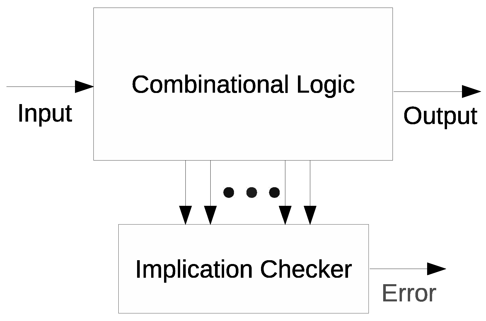
The parallel error detection using implications is illustrated in
Figure 1. Error signals are generated by the checkers checking these implications whenever implication relationships are violated. Since thousands of such implication relationships can exist in a circuit, it is not possible to check all the relationships, as then the additional checker hardwares would lead to huge area and delay overheads [
10]. However, selecting only some valuable implications for checking can help detect the maximum number of errors. If such a reduced set of implications is identified precisely, it can become a powerful tool for low cost error detection. Another advantage in using implications for CED is that no knowledge of high-level behavioral constraints is required to identify these invariant relationships. Since implication-based CED cannot guarantee 100 % error coverage, it is more useful in those applications where a perfect operation is desirable but not mandatory. CED using implications is very flexible, as some previous studies [
10,
14] describe additional techniques for enhancing
through methodological inclusion of more implications.
However, in the selection of a reduced set of valuable implications, the existing works are not able to consider all of the errors in a circuit, which are observable at the outputs due to considering only a subset of the total input space of the target circuit. Hence, in this paper, we present an approach using automatic test patterns to more exactly target those invariant relationships which are considered valuable for the whole input space. To this end, the article makes the following contributions.
We present a method based on Automatic Test Pattern Generation (ATPG) for determining the number of errors detected by each implication, which enables an improved selection of a reduced valuable set of implications for achieving maximum .
We use circuits implemented in Field Programmable Gate Arrays (FPGAs) for experimentation, which makes the testing more representative of how implications would perform in an implemented circuit rather than operating on netlists based in simple logic gates.
We present a method based in ATPG for fast and judicious estimation of .
3. Input Vulnerability-Aware Detection
As stated in the previous section, to efficiently select a reduced set of implications, all of the input space should be considered in the evaluation. This, however, is impractical when there are a large number of inputs vectors for a target circuit.
It should be noted that the entire input space does not hold equal significance as some portion of the input space is more vulnerable to errors than the rest [
16,
17] (i.e., the portion of the input space which makes the maximum number of errors observable at the primary outputs). During the process of generating 32,000 random vectors for assigning detectability to each implication, some of the vectors could be selected from the portion of the input space, which is less vulnerable to errors. Then, the implication selection will be biased towards those implications which perform better for the randomly selected 32,000 input vectors. This means that the implication which is being considered as having the highest detectability for a fault may not be in fact the best choice for that fault.
Thus, instead of using 32,000 randoms vectors in the realization of prime implications, we explore the use of a specified input space [
16] that is most vulnerable to errors. Input-aware vectors in compressed form can be obtained for each fault using an ATPG like ATALANTA [
18] which is a publicly available ATPG tool based on the fan-out oriented (FAN) algorithm. For bigger circuits, FAN algorithm limits an ATPG’s search space to reduce its computation time [
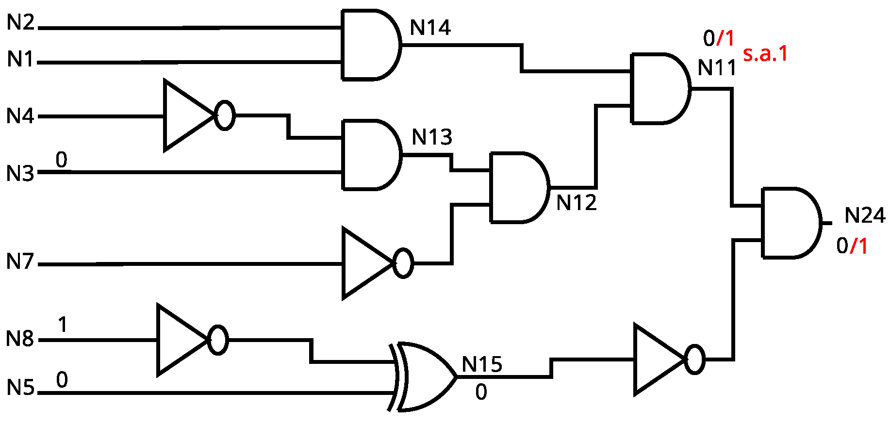
19]. Using ATALANTA’s test generation system, we can generate all possible test patterns for each fault, as shown in
Figure 4, to identify the most susceptible areas of the circuit. The tool generates all the test vectors in a compact form after performing fault simulations on each node of the circuit which can then also be processed in their compressed form.
These vectors that make the errors associated with a fault observable at the primary outputs (POs) are generated using the ATPG tool. For each possible fault in the circuit, we will then consider these input patterns for a more accurate selection of implications. This approach thus allows us to emphasize only those input vectors for each fault that make all the errors due to this fault observable at the POs which helps in an accurate detectability estimation for each implication.
Table 1 shows how implications are selected using an example case of a three input circuit. The PO is labeled as
O. We must select one implication out of the following two implications,
and
, where
A and
B are any two wires in the circuit. Let us assume that the stuck-at-1 (s.a.1) fault at some internal wire propagates to the output
O at the input vectors
. Our goal is to select an implication which has the maximum detectability in this case. Between
and
,
is able to detect the given fault whenever the associated error is observable at the output, whereas
cannot detect the error observable at 110, since
is not enabled at this input vector. Clearly,
is preferable for the given s.a.1 fault. The problem lies in only using a random set of vectors in grading the implications. With a random set of vectors, we might select
over
which also performs well but does not have the highest detectability for the fault under consideration given the total input space. This is because, for circuits with a large input space, the use of random vectors does not guarantee that a majority of fault-aware vectors are employed in assigning the detectability to an implication.
4. Proposed Methodology
The first step in implications based concurrent error detection is to actually discover invariant relationships between the different wires of a circuit. Since considering all these implications would result in huge hardware overheads, we must only select the most valuable implications such that a high is achieved at minimum hardware costs. This makes implication selection the most crucial step in implications enabled CED. Moreover, the purpose of using implications in the first place is to enable CED at low hardware costs.
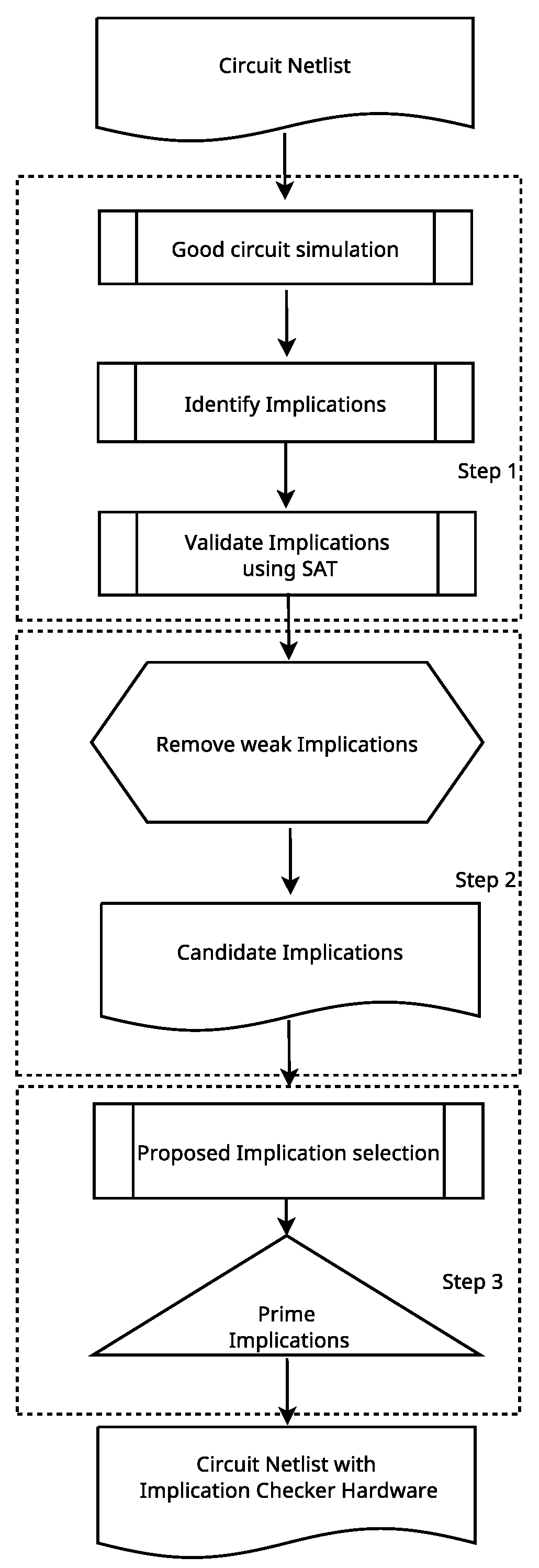
The proposed algorithm ensures selection of the most valuable implications accurately through automatic test pattern generation tools rather than relying on 32,000 random vectors based circuit simulation. The flow of our algorithm is shown in
Figure 5 which includes following steps.
Identify implication relationships through good circuit simulation.
Remove potentially weak implications.
Judiciously select the most valuable implications from the remaining ones such that the maximum achievable is ensured.
4.1. Implication Identification
First, logic values of all the wires in a circuit are recorded on good circuit simulation over 32,000 random input vectors. The simulation output is then processed to extract all the potential implications. Since the implications identified until this point are only potential as the good circuit simulation is not exhaustive, we must separate valid implications from invalid ones. To this end, a formal method based in Boolean Satisfiability (SAT) is applied to the list of potential implications.
The aim of this SAT based verification is to check for any instance from the input space where the implication under test is invalid. If no such condition exists, then the implication under test is deemed valid, i.e., no such input vector exists for which the implication relationship is violated. The circuit is converted into its conjunctive normal form (CNF) [
20] and each implication is tested by constraining the circuit CNF with is violating condition and checking in the SAT engine whether there exists an input condition for which this CNF constrained with the given implication’s violating condition is satisfiable. For example, consider an implication
, the circuit CNF is constrained with its violating condition
and
. If the SAT solver fails to find a satisfying solution, this implication is non-violable for any input vector and thus is a valid implication.
4.2. Weak Implications Removal
For removal of weak implications, a probability filter is applied to the validated implications for quickly identifying and removing weak implications. In a weak implication, the implicant wire has a low probability of being excited with the proper signal value for which the implication relationship exists. Implications whose implicant node has a probability of less than 5% of having the proper logic signal according to the simulation results are discarded. This threshold value can be optimized for each circuit, however, it is kept constant for all circuits in order to quickly process the list of verified implications.
4.3. Implication Selection
For a given set of input vectors, it can be checked that whether a fault will propagate to the output and how many times a certain implication can detect the error at the POs. A bit-flip fault in FPGA when expressed as an error can behave just like a stuck-at fault. Thus, implication detection is introduced as a number which reflects how many times an implication under test is violated when the stuck-at fault is observable at the POs. The basic methodology is the same as Alves et al. [
13] which is to select one implication for each possible stuck-at fault in the circuit. This set of implications is called prime implications.
Algorithm 1 illustrates the proposed method for a more accurate selection of prime implications. This algorithm processes all the implications and selects the best implication for each fault based on their implication detectabilities. In our algorithm, several particular data structures are used, which are given in
Table 2. The implication selection process operates in an iterative manner over each fault. As outlined in Algorithm 1, for each fault, we enumerate all those vectors which make the errors associated with the given fault observable at the POs where these vectors are called test_vectors for the given fault. These vectors can be obtained in compressed wild-card patterns from an ATPG like ATLANTA [
18]. For example, a wild card *11 represents both 011 and 111 vectors. These wild card entries for each fault are then used in fault simulation of the given fault for computing the implication detectabilities new_Detectability using HOPE [
21]. HOPE can process the test_vectors in their compressed pattern form. For each fault, it considers all the implications and selects a single implication that has the highest detectability best_Detectibility for the given fault. This implication identifier together with its number of detections is saved against the fault identifier as best_imps.
The selected implications are sorted in descending order according to their associated fault detection. The implications included in this ordered list are called the prime implications. Top-candidates from the list are more likely to provide better fault coverage than implications located at the bottom of the list. Finally, with an ordered list, it is now possible to select a subset of these implications starting from the top that satisfies a given hardware budget to include in the checker logic.
Based on the same methodology, test patterns generated through ATALANTA for each fault are then used for an accurate evaluation of the selected implications in the calculation of
. Algorithm 2 explains in detail our method for
calculation. Instead of applying 32,000 pseudo-random vectors, only the test_vectors in compressed forms are applied. The implication checker hardware is added to the netlist and this netlist along with the fault list and the test vectors for each fault are provided to HOPE in order to calculate
. In Algorithm 2, TP and TM refer to True Positive and True Miss, respectively. More details on the calculation of error coverage are provided in
Section 5.3.
| Algorithm 1 Algorithm for implication selection. |
| Input: network, imp_set, faults |
| Output: best_imps |
- 1:
for in : do - 2:
test_vectors = ATALANTA(network, fault) - 3:
best_Detectability = 0 - 4:
for in : do - 5:
new_Detectability = HOPE (network, fault, test_vectors, imp_set) - 6:
if () then - 7:
best_Detectability = new_Detectability - 8:
best_imp = imp - 9:
end if - 10:
end for - 11:
best_imps[fault] = (best_imp, best_Detectability) - 12:
end for - 13:
return best_imps
|
| Algorithm 2 Algorithm for implication testing. |
| Input: network, faults, test_vectors, best_imps |
| Output: |
- 1:
TP = 0 - 2:
TM = 0 - 3:
for in : do - 4:
test_vectors = ATALANTA(network, fault) - 5:
detection = HOPE(network, fault, test_vectors, best_imps) - 6:
if () then - 7:
TP = TP + 1 - 8:
else - 9:
TM = TM + 1 - 10:
end if - 11:
end for - 12:
Calculate () - 13:
return
|
5. Experimental Methodology
The techniques described in
Section 4 were applied to a set of combinatorial MCNC benchmarks. Implication based CED can also be applied to sequential circuits [
10,
13], however, we have restricted ourselves to only combinational circuits in this work since the purpose is only to compare between our algorithm with that in Alves et al. [
13]. The main concern with regards to implication based CED in sequential logic is that of its applicability. Then, the next concern is regarding achieving sufficient
in sequential circuits. Both issues have already been evaluated in [
10,
13]. Implication-based CED can be applied to sequential circuits simply by opening all the feedback registers and turning them into primary circuit inputs, effectively transforming the sequential circuit into a combinational circuit for processing purposes Alves et al. [
13].
We have used FPGA-based netlists synthesized using the Xilinx Synthesizer Tool (XST) in our experiments. The FPGA-implemented post-synthesis netlists are used so that the performance of implication-based CED becomes more representative of implemented circuits unlike netlists based in simple logic gates, as used in [
10,
13]. It should be noted that the results achieved by implications enabled CED vary depending upon the given circuit implementation. In FPGAs alone, there could be various circuit implementations according to the type of gates in the given library. Therefore, the
results would vary even between different FPGA types. However, the expected performance improvement of our method relative to Alves et al. [
13] would remain applicable on any circuit implementation. The profiles of the circuits used in this work including their primary inputs (PIs), primary outputs and the number of look-up tables (LUTs) consumed on a Xilinx Virtex-5 XCVLX100T device are given in
Table 3.
Here, we explain how the algorithm explained in
Section 4 is realized. First, Icarus Verilog [
22] is used in good circuit simulation of the post-synthesis Xilinx verilog format netlist for a length of 32,000 pseudo-random vectors. The logic values at each wire are recorded for this duration of circuit simulation. A Python program is used to search for potential implications from the good circuit simulation output files. The potential implications are then verified in a SAT engine. We have used the PicoSAT [
23] solver for implication validation. The output of this step is a list of verified implications. The implications whose implicant node have a probability of less than 5% of having the appropriate logic value required for enabling the implication are removed according to the good circuit simulation output. The output is a list of candidate implications for selecting prime implications from. The netlist is then converted from a Xilinx verilog format to BENCH format. During conversion, the names of wires in the original LUT-based netlist are preserved so that only faults on those wires will be processed in the following steps. Next, for each stuck-at fault in the circuit, ATALANTA is used to produce the test_vectors in compressed pattern form. The fault simulator HOPE [
21] is then given the fault list, the test_vectors for each fault and the circuit netlist with the checkers for each candidate implication. HOPE is able to process the test_vectors in their compressed form. The output of this step is a simulation output for each fault containing information about the detectabilities of all the candidate implication checkers for that fault. Thus, the best implication for each fault is selected based on this output from HOPE.
The best implications for each fault are called prime implications. Next, we add the checkers for all these prime implications to the original circuit netlist and pass the modified netlist along with the list of all the possible stuck-at faults in the circuit and their test_vectors to HOPE. We then use HOPE’s fault simulation output to calculate the achieved by the prime implications.
We have compared our results with the state-of-the-art implication selection algorithm from Alves et al. [
13]. In our work, the algorithm from Alves et al. [
13] was also realized using the same tools. The model in Alves et al. [
13] differs against this work in that the implication selection step uses 32,000 pseudo-random vectors instead of the exact test_vectors for each fault. All the boolean algebra in this work was performed using the Python pyEDA module [
24].
5.1. Execution Time Evaluation
The comparison of total execution time in selection of prime implications for the benchmark circuits considered is shown in
Table 4. The experiments were performed on a linux machine running a 3.30 Ghz quad-core with 16 GB DDR3 memory. Systematic generation of compressed input patterns which are used to test implications makes the execution of the proposed algorithm faster; in fact, our algorithm takes 0.234 min on average compared to 1.09 min taken by the method in Alves et al. [
13].
In
Table 4, we also observe that two test circuits ibm and signet specifically have higher execution times in the proposed algorithm. This is due to an increased number of test vectors generated by the ATPG. Since there are many faults that do not collapse into other faults, the ATPG takes a longer time in generating the test vectors for a large number of faults.
5.2. Compression Rate Evaluation
Table 5 shows the results of implication reduction for the various benchmarks. Column 2 gives the total number of validated implications after processing the potential implications in the SAT engine. Column 3 gives our total number of selected prime implications while Column 4 gives the number of prime implications selected by Alves et al. [
13].
The compression rates depend on the benchmark circuit under consideration. At maximum, the number of selected implications will be equal to the total number of possible stuck-at faults in the circuit since only a single implication deemed best for a given fault is selected. However, when the same implication is selected for multiple faults, the selected implications count will be lower than the maximum possible.
Here, we can observe the difference between operating on a post-synthesis FPGA implemented netlist. Compared to the basic logic gates-based netlists in Alves et al. [
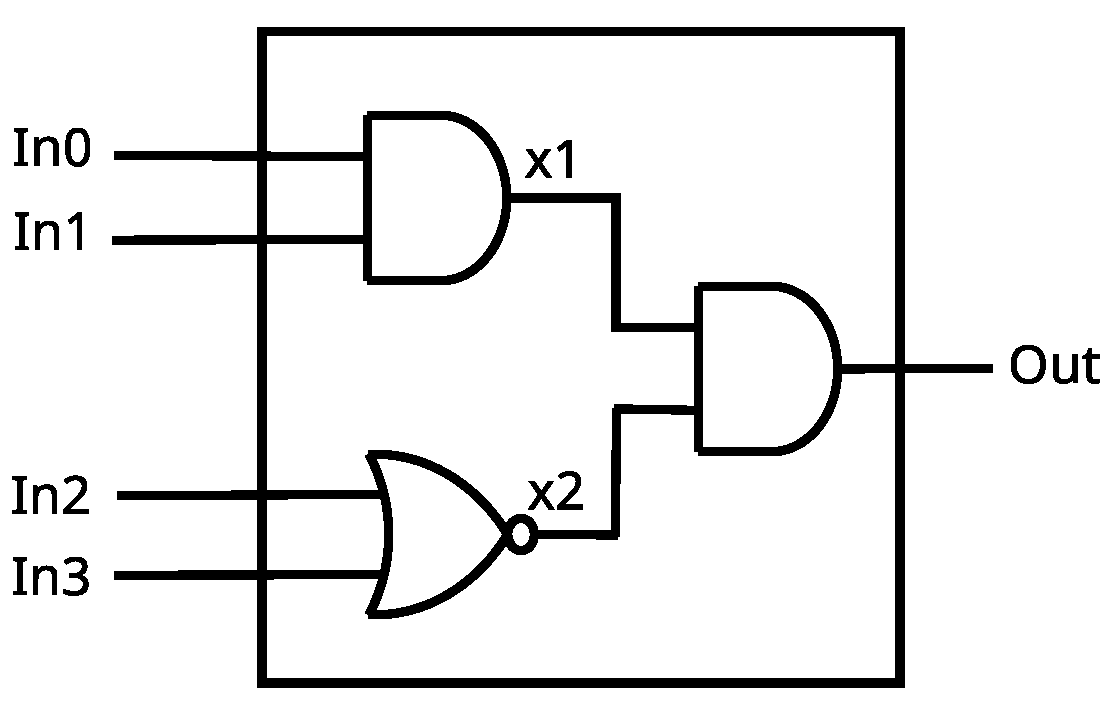
13], where the validated implications count is usually in thousands, the validated implications count on FPGA circuits is much lower. This is because there are fewer wires in a LUT-based circuit netlist compared to logic-gate based netlists. As shown in
Figure 6, wires
and
have been covered by the LUT and implemented in memory thereby reducing the number of wires available to search candidate implications from.
5.3. Evaluation
For each fault, its test_vectors are applied to the circuit under test and the response is classified into one of the following four cases:
No Effect.
True Positive (TP): Faults occur at internal node and are detected and visible at PO.
False Positive (FP): Faults occur at internal node and are detected but never modified any PO.
True Miss (TM): Undetected and modified a PO.
The false positive response is observed either when the checker hardware itself is affected by a fault or when an error occurs in the circuit under test but gets logically masked and thus is not observed at the PO. In the computation of
, we have also used the ratio (i.e.,
, as has been used in Alves et al. [
13].
The
metric for the proposed approach and for the approach in Alves et al. [
13] are compared in
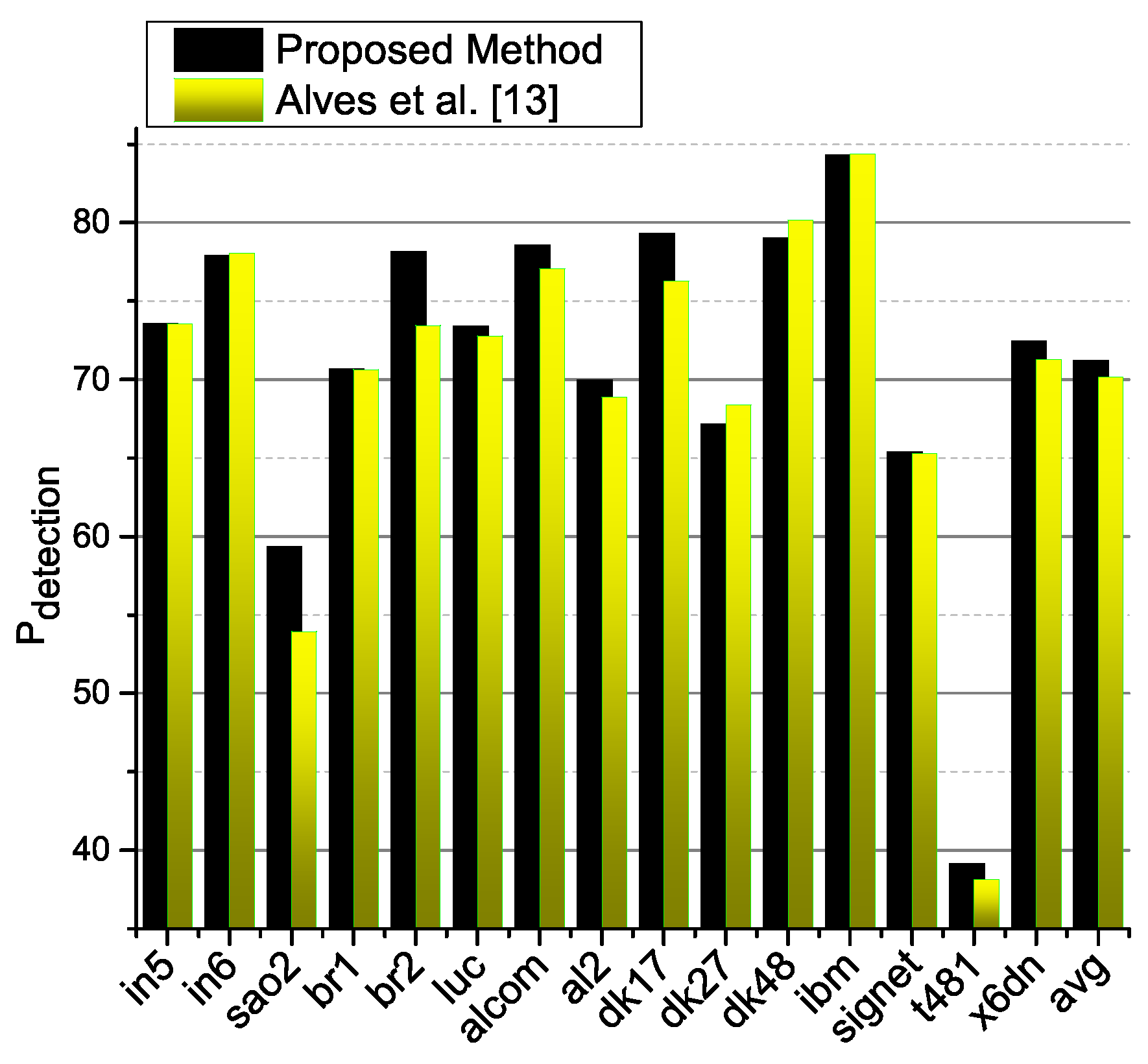
Figure 7. When the best implications are selected for each fault using the proposed method, it does not guarantee that
will increase drastically, especially in this case of FPGA circuits where the total validated implications count is already a few hundred in all of the given circuits. Even though the method based in the selection of implications from random vectors Alves et al. [
13] performs well, since it includes a heuristic step, the achieved
cannot be claimed lossless. However, in the proposed method, it is guaranteed based on the efficiency of the ATPG tool which generates the test_vectors for each fault, that the achieved
could be optimal. This can be checked by looking for an instance where the method proposed in Alves et al. [
13] selects a number of prime implications less than our proposed method and achieves a higher
. By observing
Figure 7 and
Table 5, we see that no such instance exists. In fact, in most cases, the
achieved by our algorithm is either higher than Alves et al. [
13] or it is almost the same for both methods. Moreover, it was shown with a case study in [
10] that even 1% degradation in
could cause millions of undetected errors thereby emphasizing the importance of even small gains in
.
This reflects the increased accurateness of the proposed method. Note that the insignificant decrease in
in some cases is due to the accuracy of the yield of the ATPG. For instance, dk27 and dk48 have only 1.2% and 1.1% higher
for Alves et al. [
13], respectively, than the proposed methodology. In the given algorithm FAN, tests are generated for each testable fault using backtracks. Due to a limited number of attempts in backtracking, the algorithm stops when a given threshold is exceeded for a fault. Then, such faults are referred to as aborted faults. For circuits such as in6, br1, dk27, dk48 and ibm, there are certain untestable faults due to which their exact test vectors are unavailable. It was shown by Fujiwara and Shimono [
25], that the yield achieved of faults that are tested using FAN is usually 95.74–99.52%. However, the average (avg)
of the proposed methodology is better compared to Alves et al. [
13]. Moreover, FAN can be replaced with more efficient test pattern generation algorithms for further minimizing any loss on
.
Thus, the proposed methodology is flexible and not only it can achieve a better average , it is guaranteed to be optimal given the accuracy of the ATPG employed.
5.4. Area and Delay Overheads
All the circuits were synthesized using the Xilinx XST tool for a Virtex-5 FPGA device. In
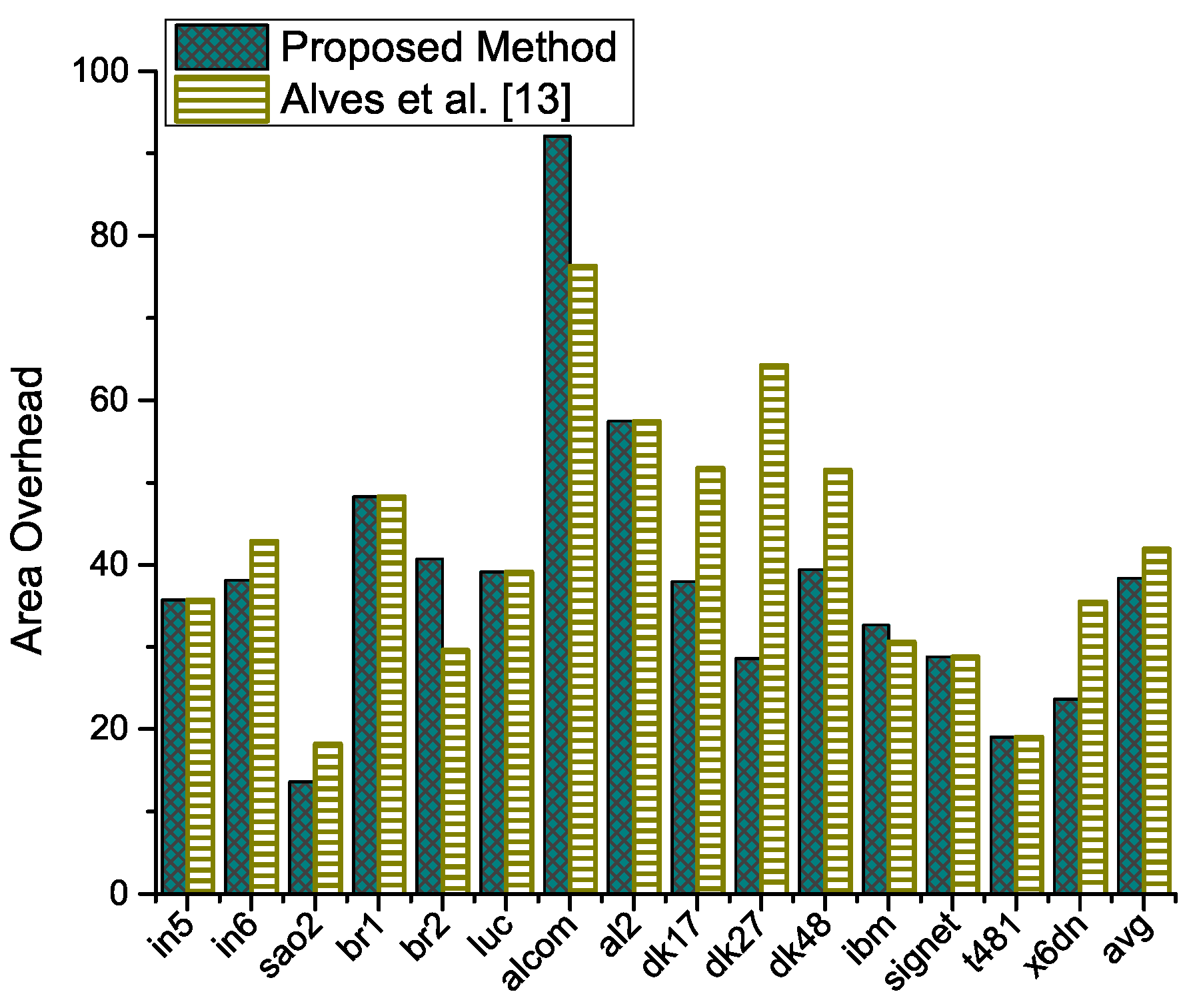
Figure 8, we show the area overhead for each benchmark we have considered when the checkers for the implications selected by both methods are included. The area overhead is calculated in terms of the number of LUTs occupied on the device. On average our method outperforms the method in Alves et al. [
13]. We have achieved a higher average
while our average area overhead is also lower than the method in Alves et al. [
13]. We must mention here that the focus of this work is to minimize the loss on
and the same methodology can also be applied to the selection of essential implications in [
10].
In
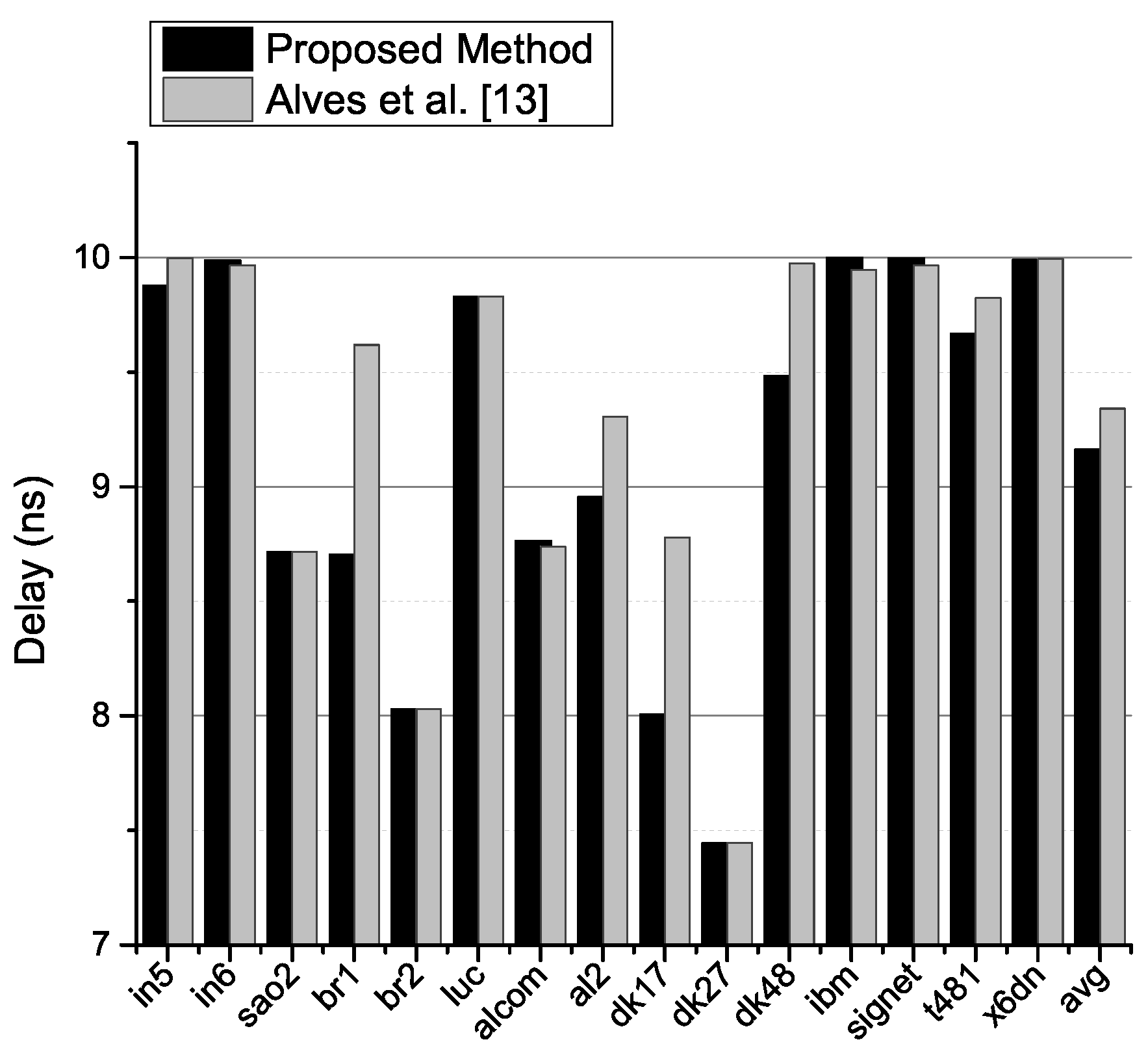
Figure 9, the delay of the circuits after the inclusion of the checker circuitry is compared. We observe that in those cases where the method in Alves et al. [
13] has achieved a higher circuit delay such as br1, al2, dk17 and dk48, the difference is very significant. On the other hand, in circuits such as in6, alcom, ibm and signet, where our method achieves a higher delay, the increase is only very slight. Thus, we do obtain a lower circuit delay on average. It must however be noted that in this work, we do not consider circuit delays as a parameter in the implication selection procedure, rather only the detectabilities of implications are considered. For example, the circuit in6 shows a slightly higher delay with our method even though the number of implications selected by our algorithm are significantly lower than that in [
13]. This is because, despite a lower implication count, there are more implications on the critical path of the circuit causing an increase in the circuit delay compared to the method in [
13]. It is possible to include the circuit delay as a parameter in the implication selection step so that a set of implications optimized with regards to circuit delay is obtained as shown in delay-optimized implication selection results [
13].
5.5. Relationship between and Selected Implications
To see the implication selection impact on
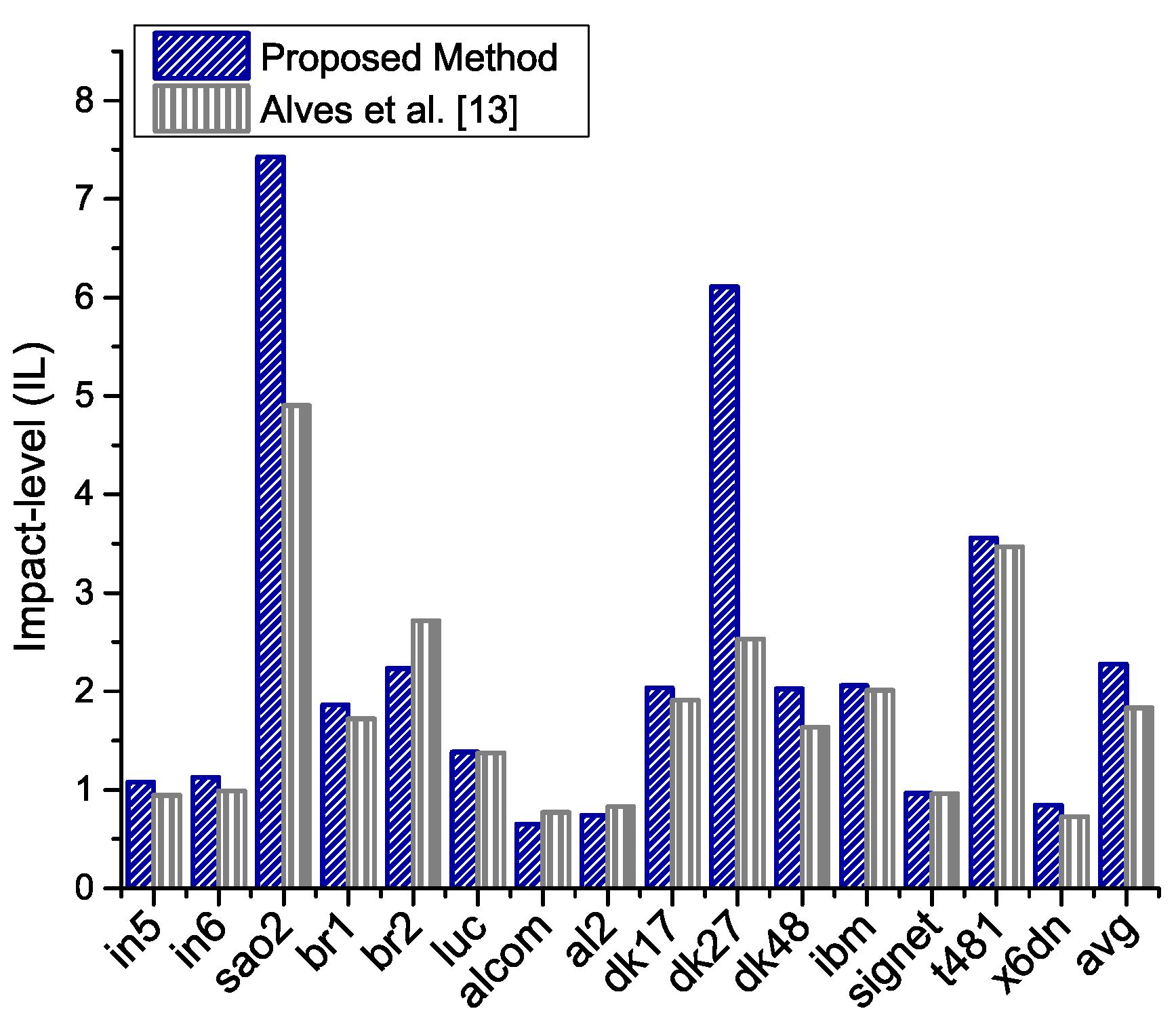
, we propose a new metric called impact-level (IL). We define IL as the ratio of
to selected prime implications count. Clearly, a higher value of IL is desirable and translates into a better implication selection. It can be seen in
Figure 10 that the proposed method has a higher impact-level. In fact, in some cases, it is much better than Alves et al. [
13]. For dk27, with a significant decrease in area overhead, we are able to improve IL by 41.10% compared to Alves et al. [
13]. On average, IL of the proposed approach is better for the given benchmark circuits.
