Recent Advances in FPGA Reverse Engineering


Abstract
1. Introduction
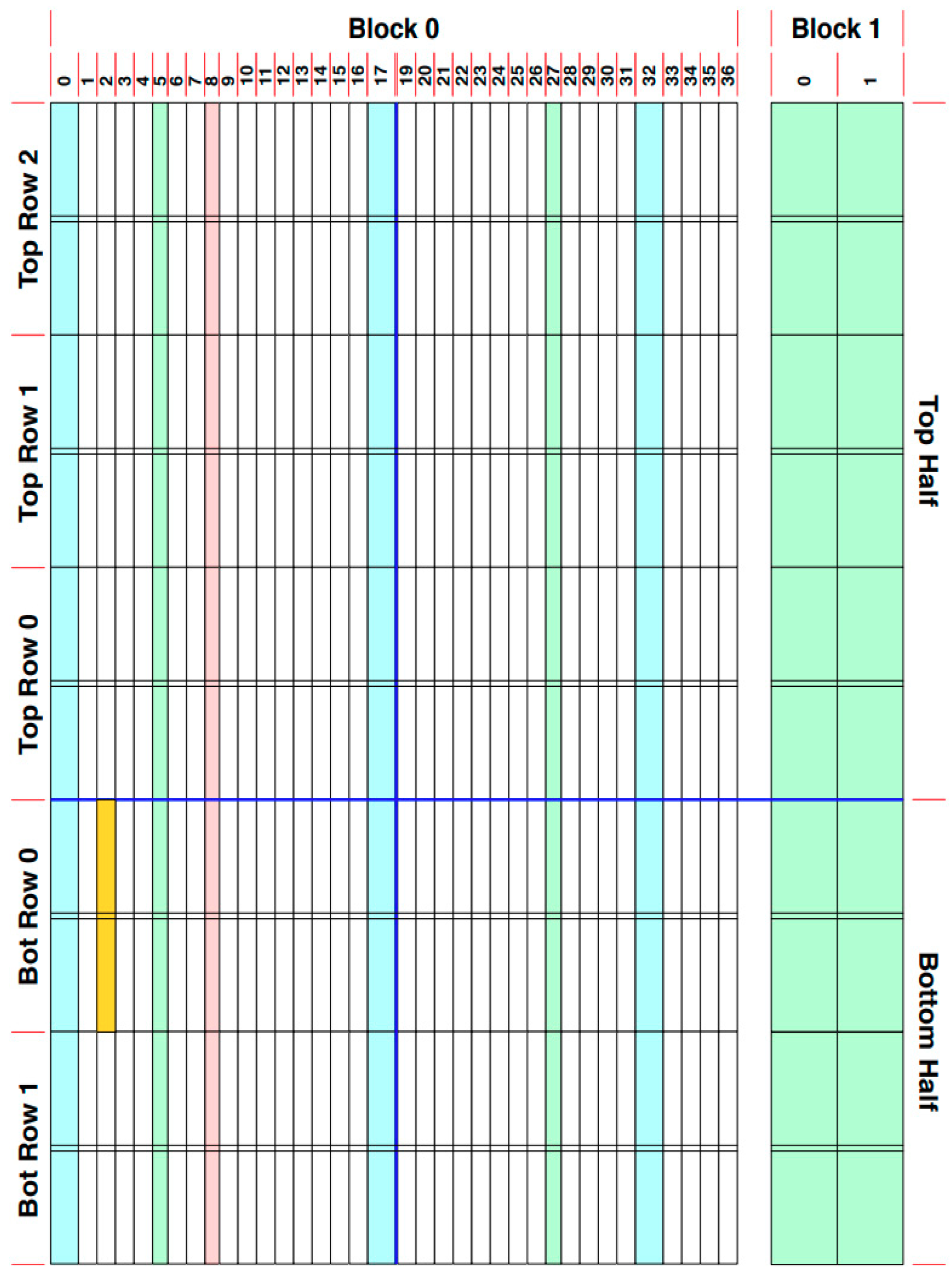
2. Xilinx FPGA Design
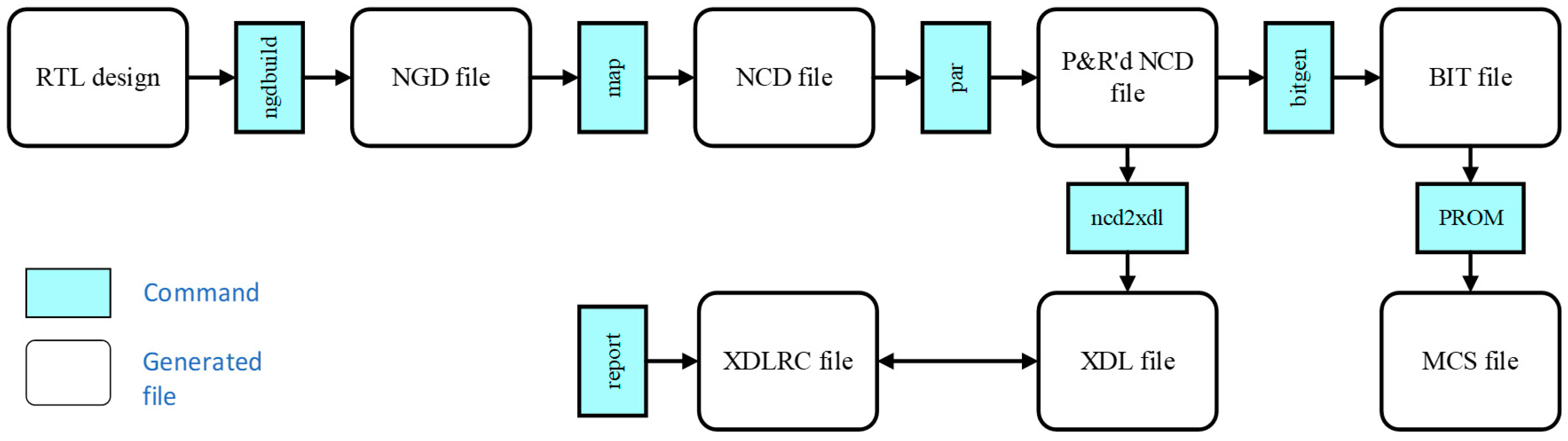
2.1. ISE Design Flow
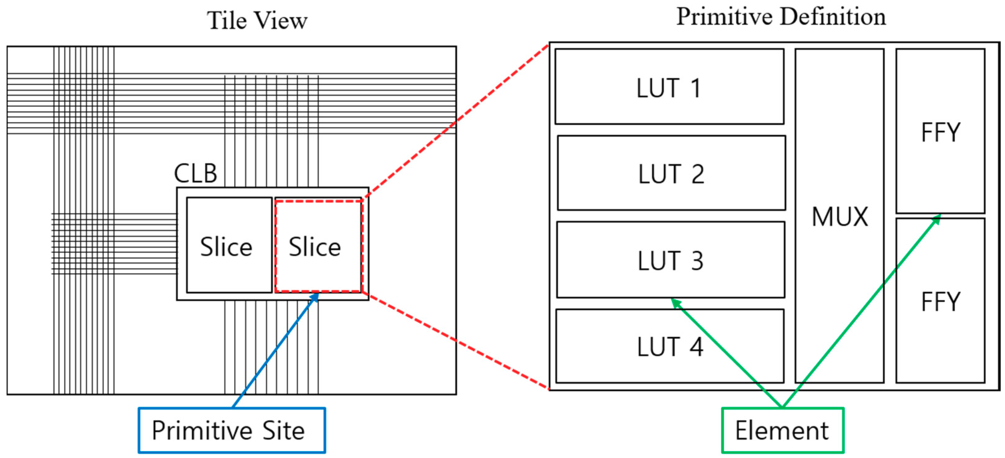
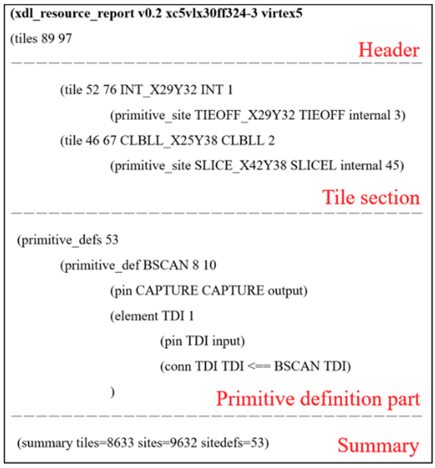
2.2. XDLRC
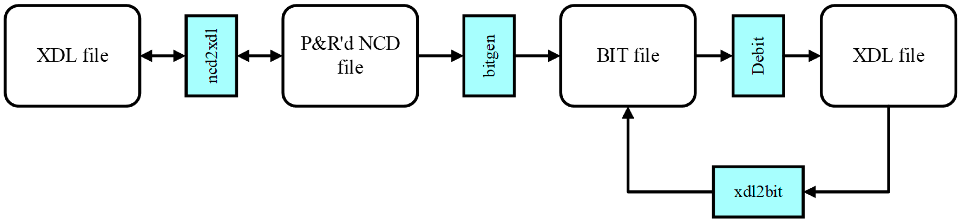
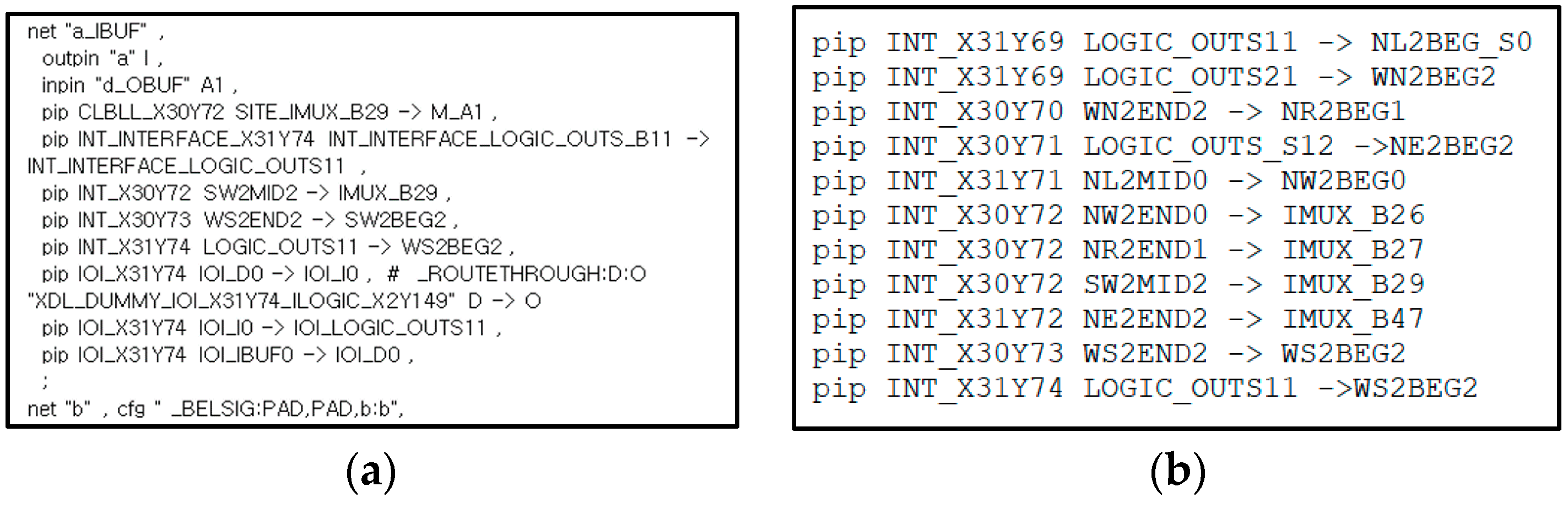
2.3. XDL
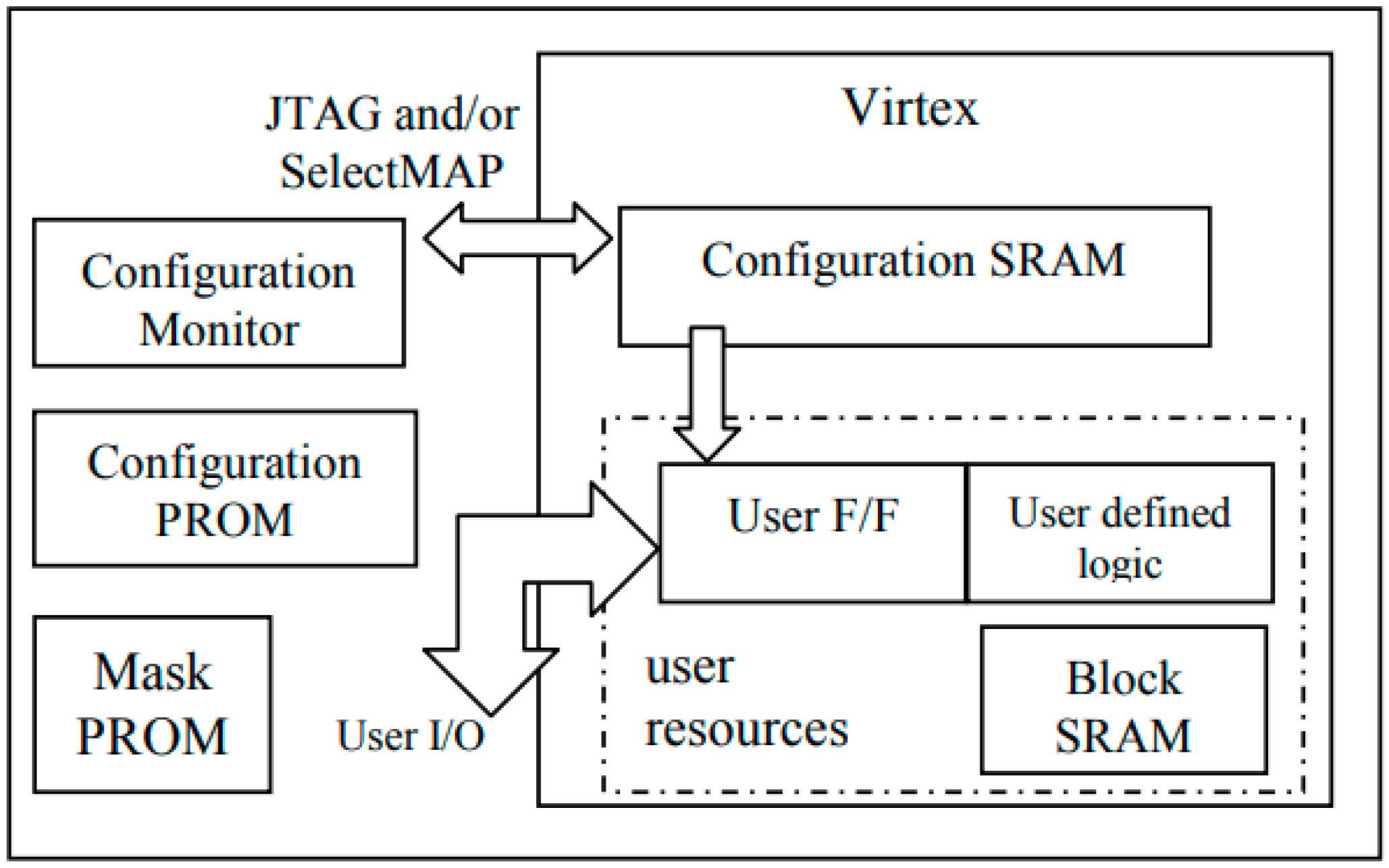
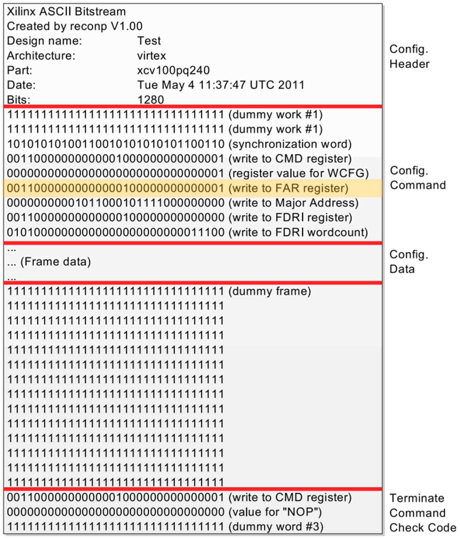
2.4. Bitstream Structure
3. Reverse Engineering Tool with Xilinx FPGAs
3.1. Debit
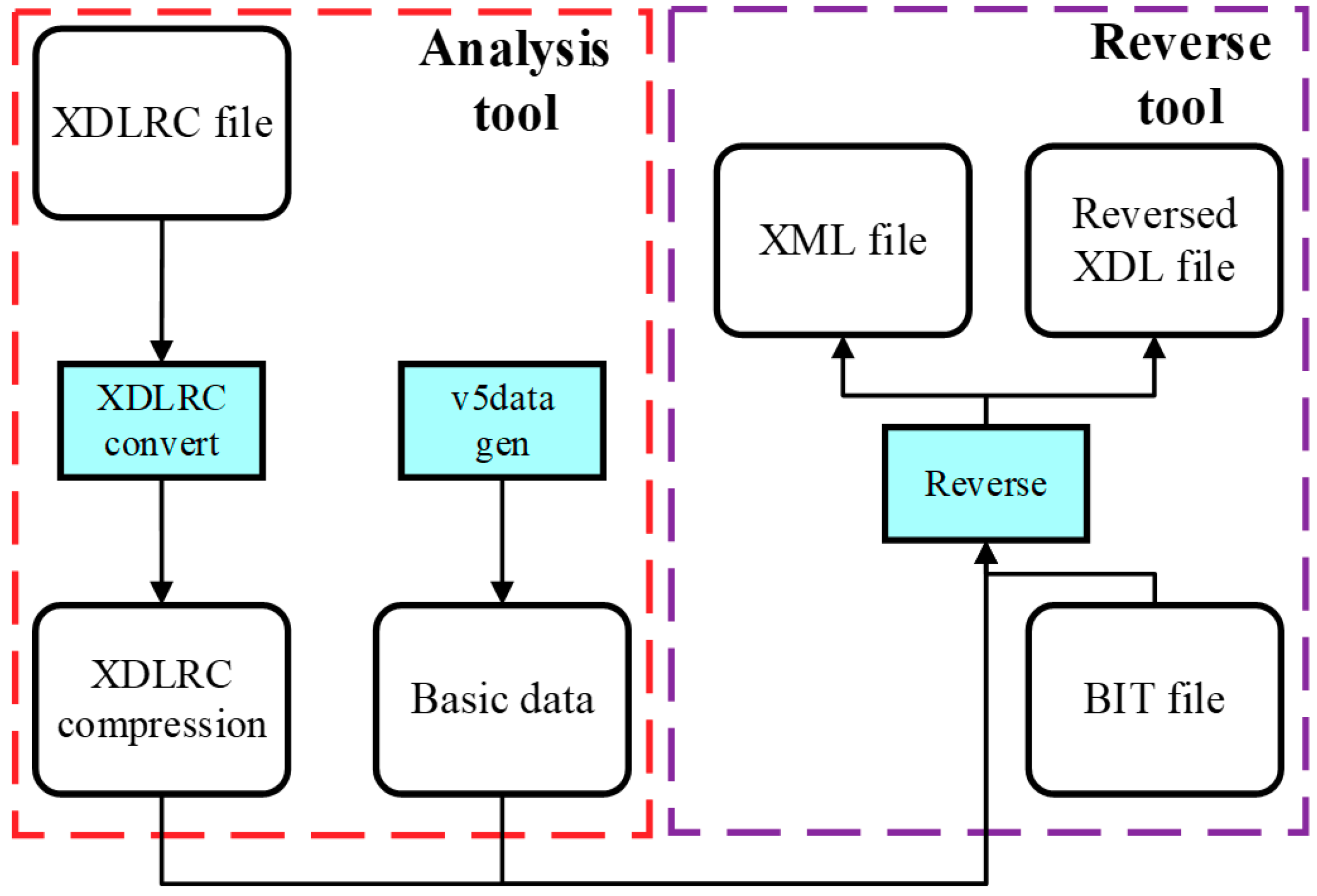
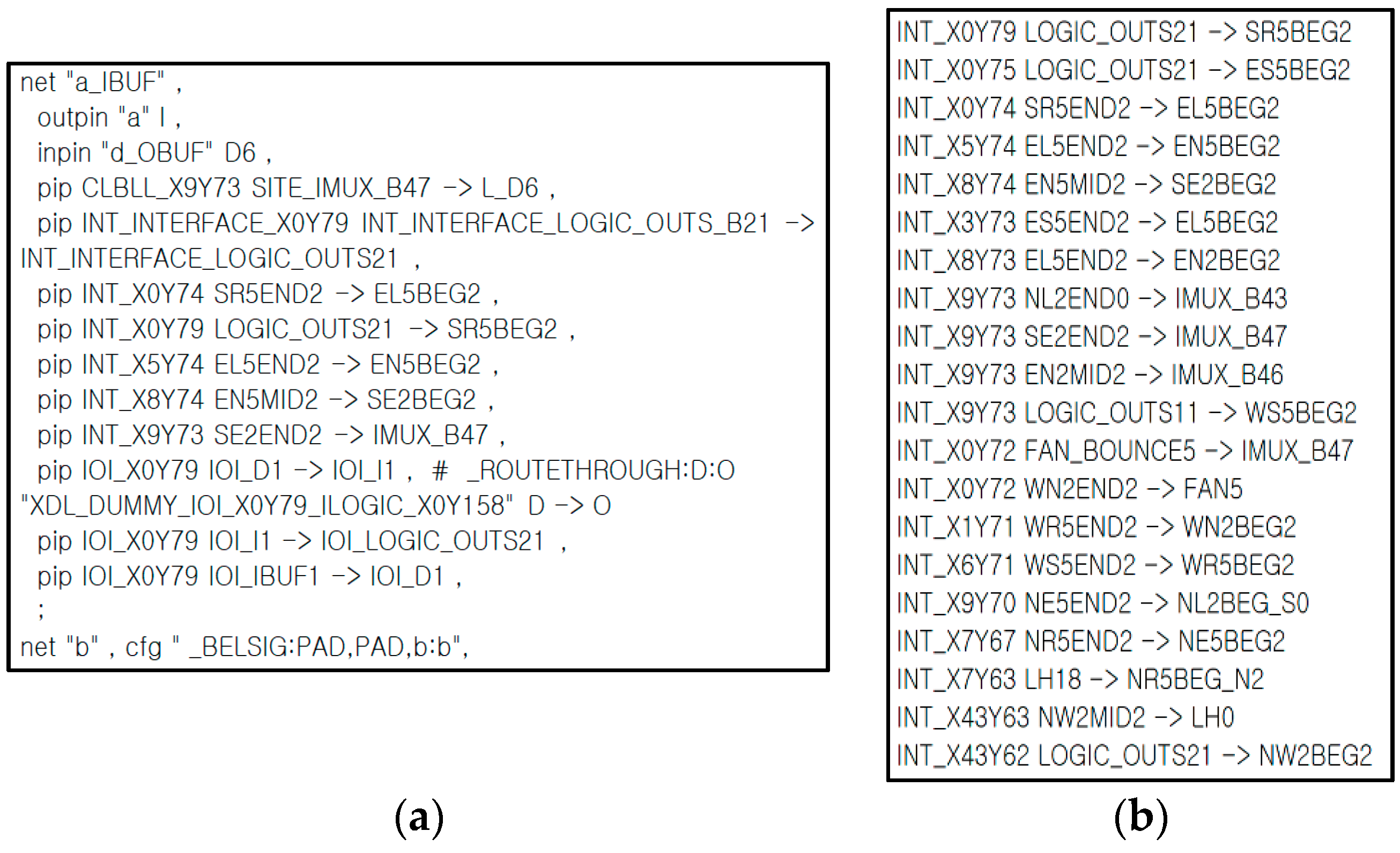
3.2. Bitstream Interpretation Library (BIL)
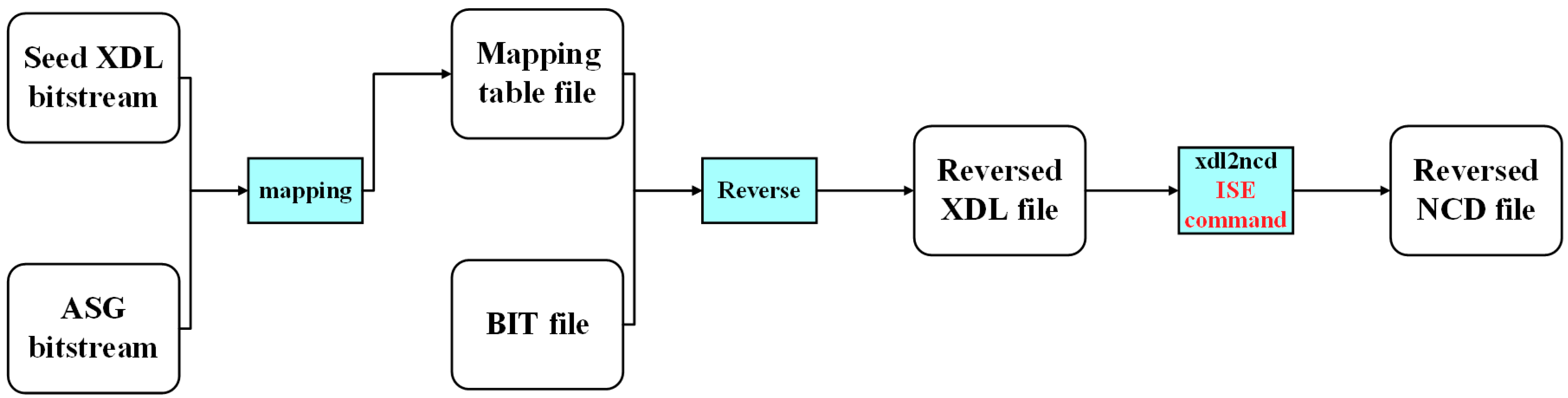
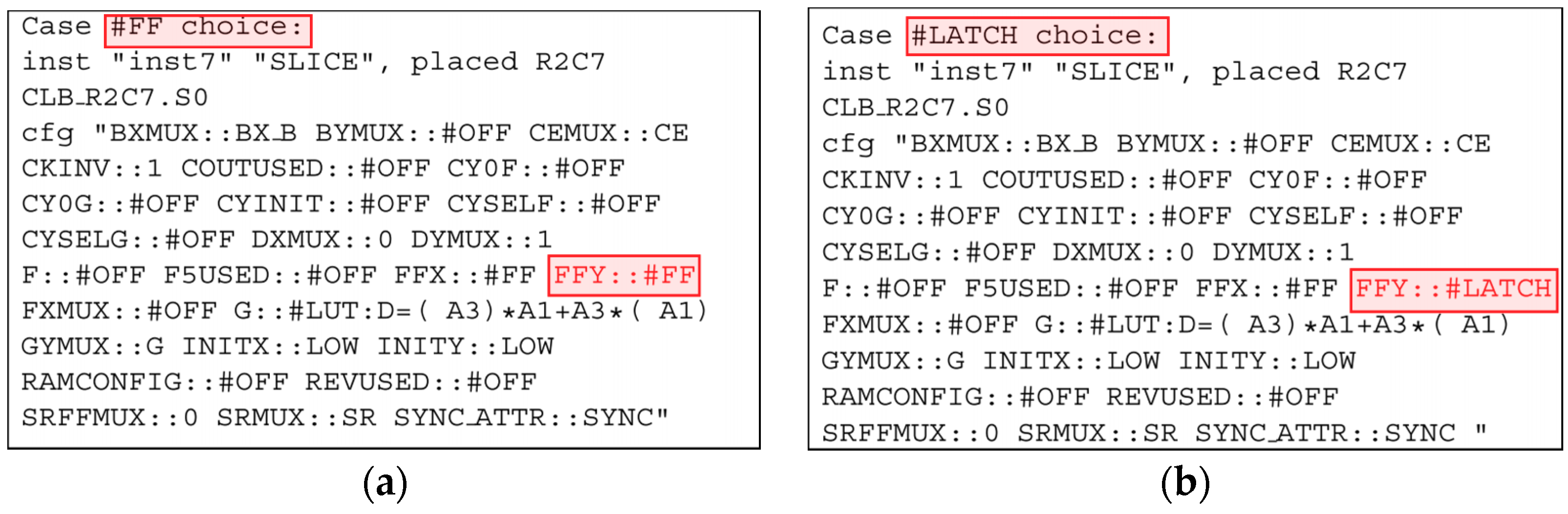
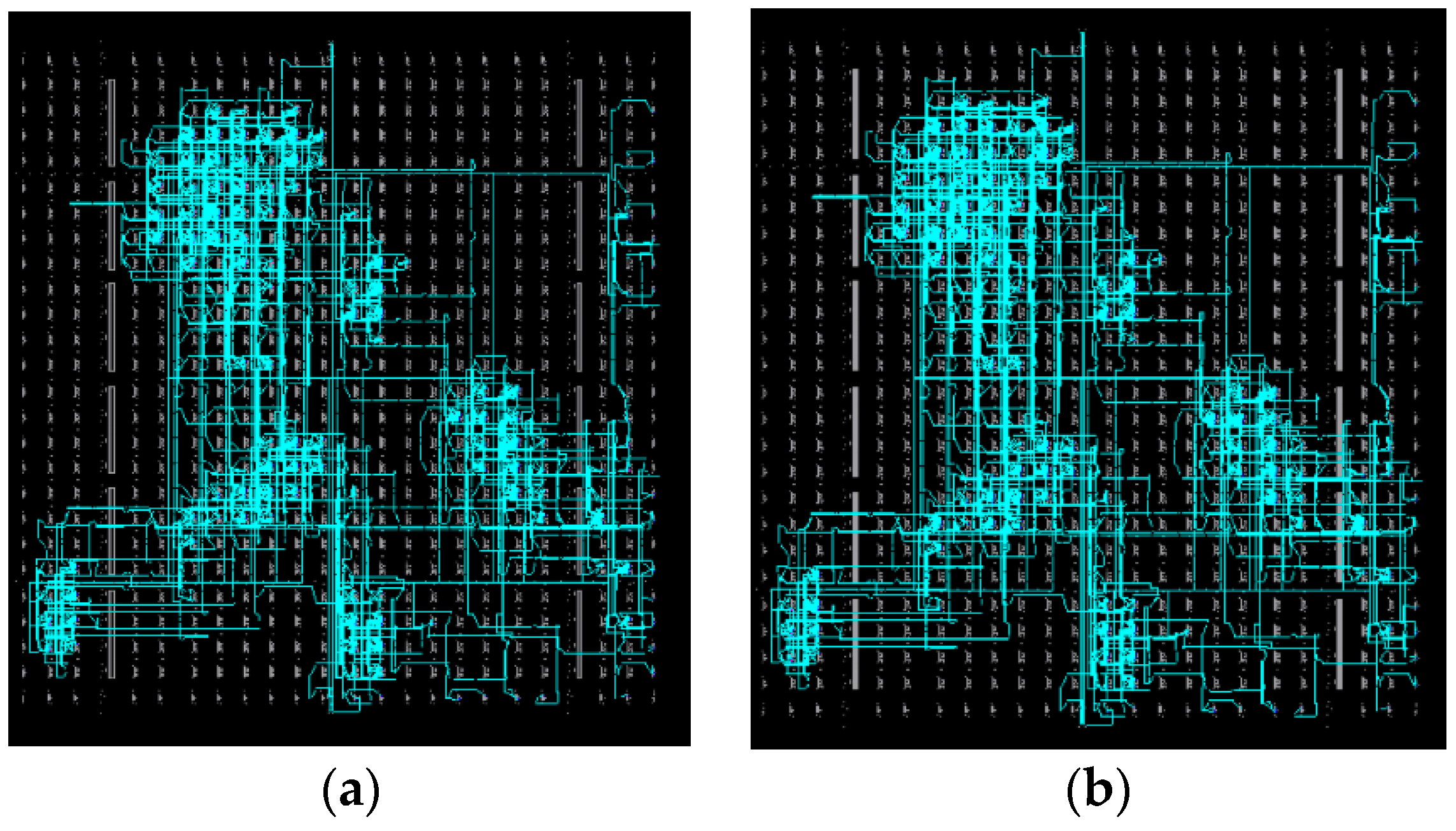
3.3. Bit2ncd
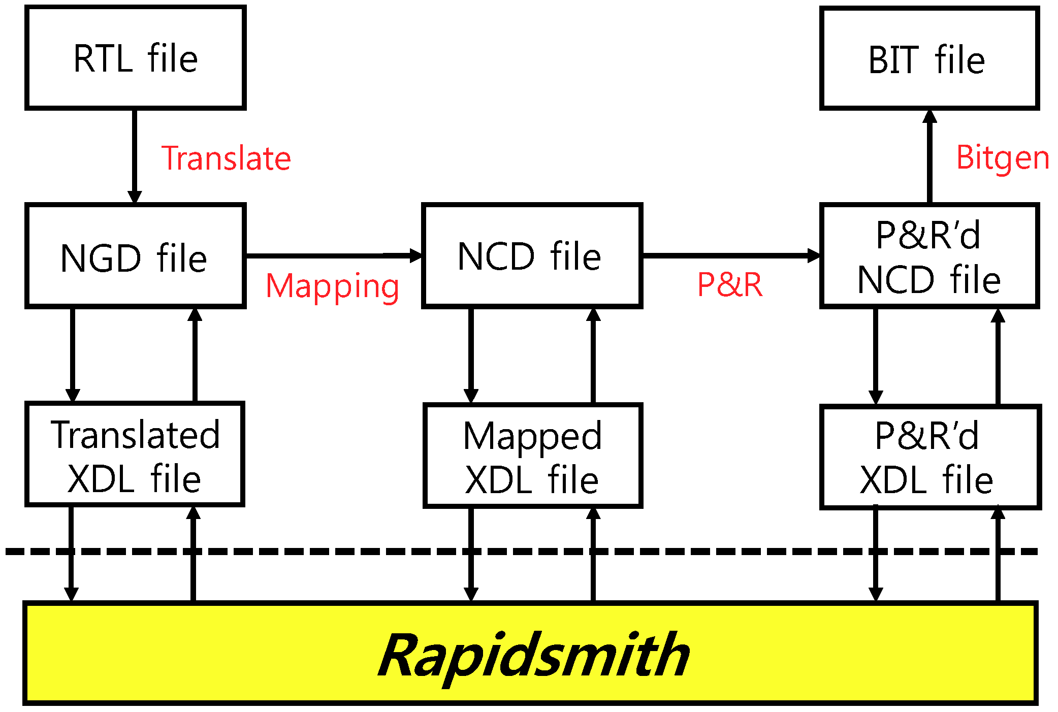
3.4. Supplementary Tool Using XDL: Rapidsmith
4. Reverse Engineering Tools with Non-Xilinx FPGAs
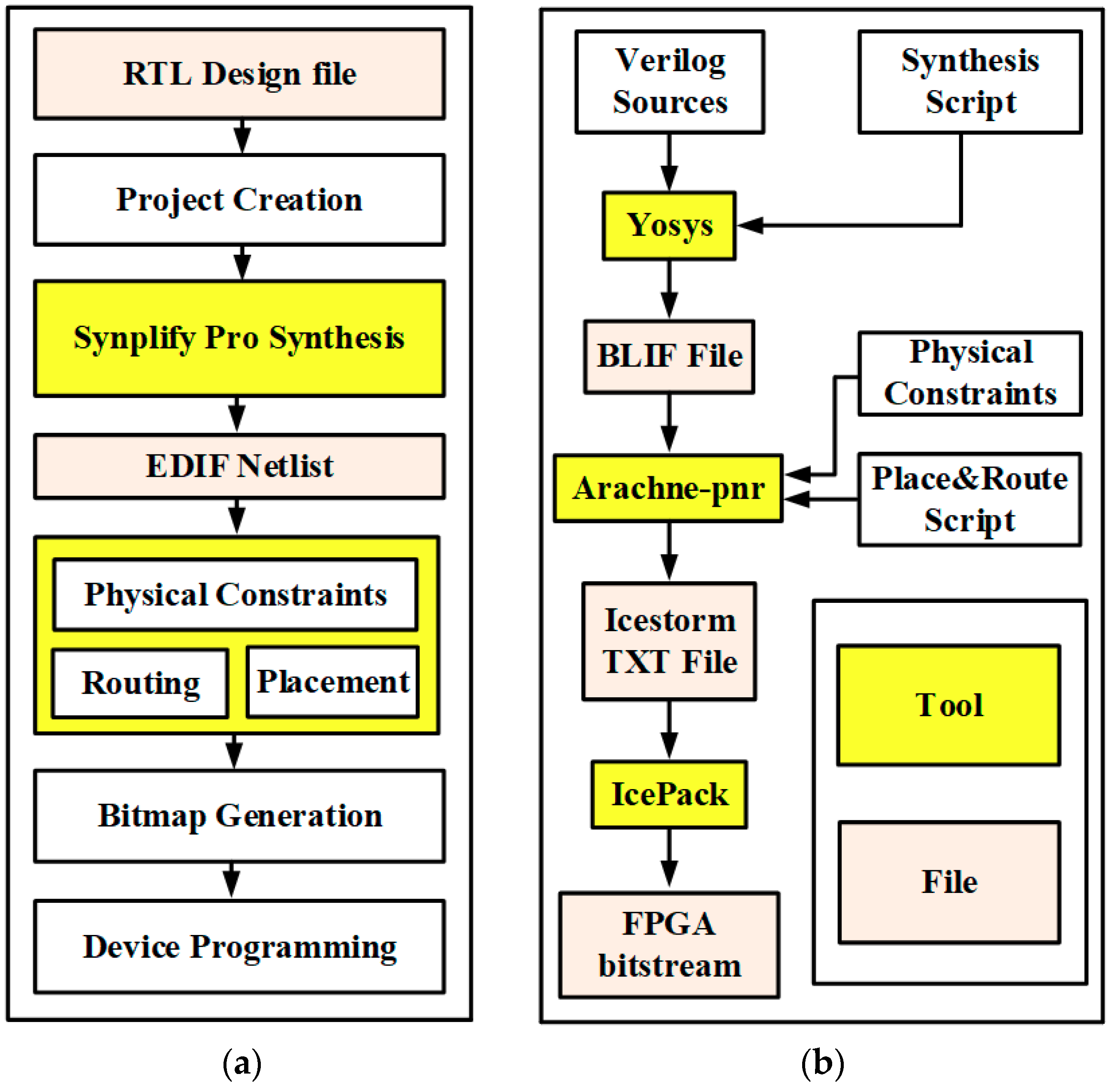
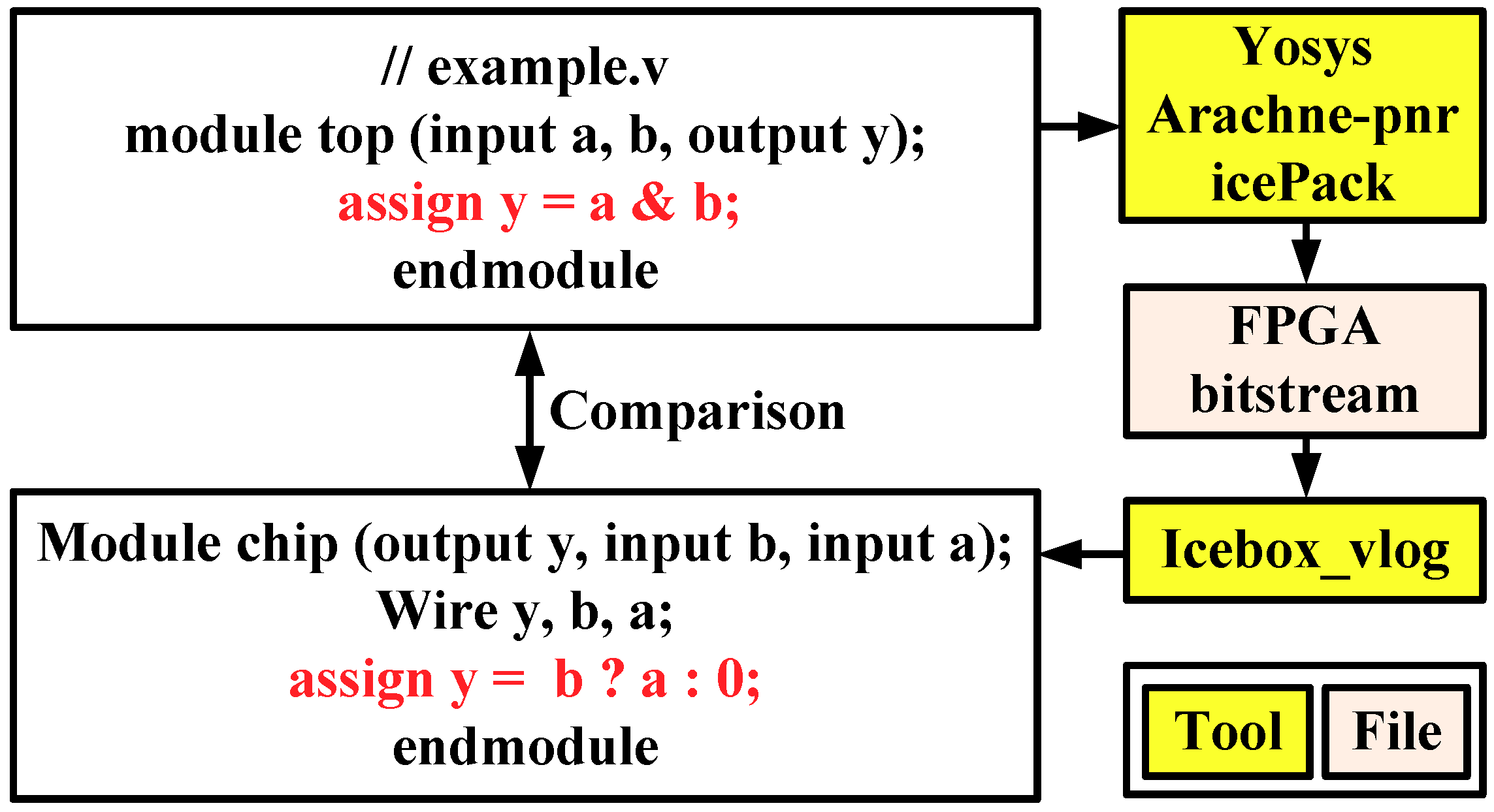
4.1. Icestorm with Lattice FPGAs
4.2. QUIP with Altera FPGA
5. Discussion
6. Conclusions
Author Contributions
Funding
Conflicts of Interest
References
- Fong, R.J.; Harper, S.J.; Athanas, P.M. A versatile framework for FPGA field updates: an application of partial self-reconfiguration. In Proceedings of the IEEE International Workshop on Rapid Systems Prototyping, San Diego, CA, USA, 9–11 June 2003; pp. 117–123. [Google Scholar]
- Virtex-5 FPGA Configuration User Guide. 2017. Available online: https://www.xilinx.com/support/documentation/user_guides/ug191.pdf (accessed on 18 September 2018).
- Lee, J.-K.; Jhang, K.-S.; Cho, H.-J. Verilog functional model extraction from FPGA design data. J. KIISE: Comput. Pract. Lett. 2012, 18, 380–388. [Google Scholar]
- Note, J.-B.; Rannaud, É. From the bitstream to the netlist. In Proceedings of the International ACM/SIGDA Symposium on Field Programmable Gate Arrays (FPGA), Monterey, CA, USA, 24–26 February 2008; Volume 18, p. 264. [Google Scholar]
- Benz, F.; Seffrin, A.; Huss, S.A. Bil: A tool-chain for bitstream reverse-engineering. In Proceedings of the International Conference on Field Programmable Logic and Applications (FPL), Oslo, Norway, 29–31 August 2012; pp. 735–738. [Google Scholar]
- Ding, Z.; Wu, Q.; Zhang, Y.; Zhu, L. Deriving an NCD file from an FPGA bitstream: Methodology, architecture and evaluation. Microprocess. Microsyst. 2013, 37, 299–312. [Google Scholar] [CrossRef]
- Project IceStorm. Available online: http://www.clifford.at/icestorm (accessed on 18 September 2018).
- Wolf, C. A free and Open Source Verilog-to-Bitstream Flow for iCE40 FPGAs. Online Presentation. 2015. Available online: https://media.ccc.de/v/32c3-7139-a_free_and_open_source_verilog-to-bitstream_flow_for_ice40_fpgas (accessed on 18 September 2018).
- Yosys Open Synthesis Suite, Online Tutorial. Available online: http://www.clifford.at/yosys (accessed on 18 September 2018).
- Romanov, A.; Romanov, M.; Kharchenko, A. FPGA-based control system reconfiguration using open source software. In Proceedings of the IEEE Conference of Russian Young Researchers in Electrical and Electronic Engineering (EIConRus), St. Petersburg, Russia, 1–3 February 2017. [Google Scholar]
- Yui, C.C.; Swift, G.M.; Carmichael, C.; Koga, R.; George, J.S. SEU mitigation testing of Xilinx Virtex II FPGAs. In Proceedings of the IEEE Radiation Effects Data Workshop, Monterey, CA, USA, 25–25 July 2003; pp. 92–97. [Google Scholar]
- Moradi, A.; Barenghi, A.; Kasper, T.; Paar, C. On the vulnerability of FPGA bitstream encryption against power analysis attacks. In Proceedings of the ACM Conference on Computer and Communications Security, Chicago, IL, USA, 17–21 October 2011; pp. 111–124. [Google Scholar]
- Lavin, C.; Padilla, M.; Lundrigan, P.; Nelson, B.; Hutchings, B. Rapid prototyping tools for FPGA designs: Rapidsmith. In Proceedings of the International Conference on Field-Programmable Technology, Beijing, China, 8–10 December 2010. [Google Scholar]
- Lavin, C.; Padilla, M.; Lamprecht, J.; Lundrigan, P.; Nelson, B.; Hutchings, B. Rapidsmith: Do-it-yourself CAD tools for Xilinx FPGAs. In Proceedings of the International Conference on Field Programmable Logic and Applications, Chania, Greece, 5–7 September 2011. [Google Scholar]
- Malhotra, S.; Borer, T.; Singh, D.; Brown, S. The Quartus University Interface Program: Enabling advanced FPGA research. In Proceedings of the IEEE International Conference on Field-Programmable Technology, Brisbane, NSW, Australia, 6–8 December 2004; pp. 225–230. [Google Scholar]
- Soni, R.K.; Steiner, N.; French, M. Open-source bitstream generation. In Proceedings of the IEEE International Symposium on Field-Programmable Custom Computing Machines, Seattle, WA, USA, 28–30 April 2013; pp. 105–112. [Google Scholar]
- Tavaragiri, A.; Couch, J.; Athanas, P. Exploration of FGPA interconnect for the design of unconventional antennas. In Proceedings of the ACM/SIGDA International Symposium on Field Programmable Gate Arrays, Monterey, CA, USA, 27 February–1 March 2011; pp. 219–226. [Google Scholar]
- Söll, O.; Korak, T.; Muehlberghuber, M.; Hutter, M. EM-based detection of hardware trojans on FPGAs. In Proceedings of the IEEE International Symposium on Hardware-Oriented Security and Trust, Arlington, VA, USA, 6–7 May 2014. [Google Scholar]
- iCE40 LP/HX Family Data Sheet. Available online: http://www.latticesemi.com/en/Products/FPGAandCPLD/iCE40 (accessed on 18 September 2018).
- iCEcube 201708 Tutorial. Available online: http://www.latticesemi.com/Products/DesignSoftwareAndIP/FPGAandLDS/iCEcube2 (accessed on 18 September 2018).
- Krieg, C.; Wolf, C.; Jantsch, A. Malicious LUT: A stealthy FPGA trojan injected and triggered by the design flow. In Proceedings of the International Conference on Computer-Aided Design (ICCAD), Austin, TX, USA, 7–10 November 2016. [Google Scholar]


| Column Type | Width in Frames |
|---|---|
| CLB | 36 |
| DSP | 28 |
| Block RAM | 30 |
| IOB | 54 |
| Tool | Input | Output | Supported Device | Pros | Cons |
|---|---|---|---|---|---|
| Debit | BIT file | XDL file | Virtex-2,3,4,5/Spartan-3 | Simple | Low accuracy |
| BIL | XDLRC, XDL, BIT file | XDL file XML file | Virtex-5 | Perfect reversing pip in INT tile | Low accuracy |
| Bit2ncd | BIT file | XDL file NCD file | Spartan-3,3E/Virtex-2,4,5 | Perfect reversing all tile types | Long time |
| Rapidsmith | XDL file, XDLRC file | XDL file | All devices | Flexible | Depending on other tools |
| Icestorm | BIT file | Verilog file | Ice40 | High accuracy | Limited target devices |
© 2018 by the authors. Licensee MDPI, Basel, Switzerland. This article is an open access article distributed under the terms and conditions of the Creative Commons Attribution (CC BY) license (http://creativecommons.org/licenses/by/4.0/).
Share and Cite
Yu, H.; Lee, H.; Lee, S.; Kim, Y.; Lee, H.-M. Recent Advances in FPGA Reverse Engineering. Electronics 2018, 7, 246. https://doi.org/10.3390/electronics7100246
Yu H, Lee H, Lee S, Kim Y, Lee H-M. Recent Advances in FPGA Reverse Engineering. Electronics. 2018; 7(10):246. https://doi.org/10.3390/electronics7100246
Chicago/Turabian StyleYu, Hoyoung, Hansol Lee, Sangil Lee, Youngmin Kim, and Hyung-Min Lee. 2018. "Recent Advances in FPGA Reverse Engineering" Electronics 7, no. 10: 246. https://doi.org/10.3390/electronics7100246
APA StyleYu, H., Lee, H., Lee, S., Kim, Y., & Lee, H.-M. (2018). Recent Advances in FPGA Reverse Engineering. Electronics, 7(10), 246. https://doi.org/10.3390/electronics7100246