
Gate Stability of GaN-Based HEMTs with P-Type Gate


 and
and 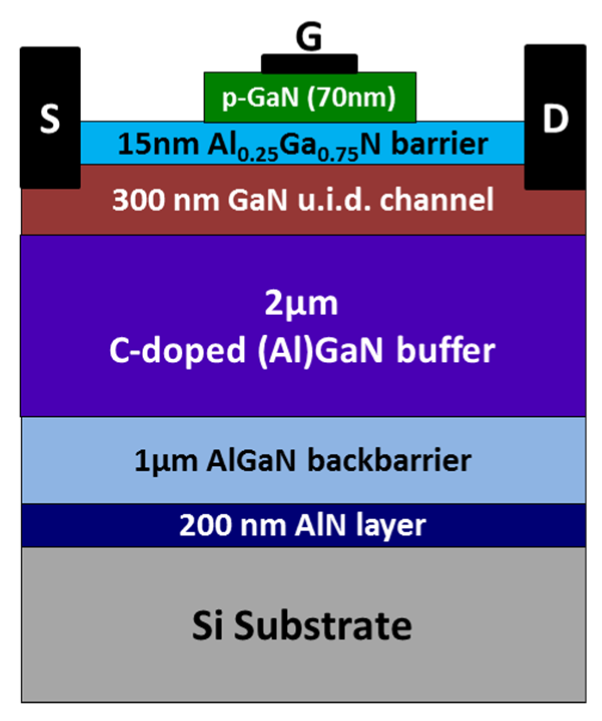
Abstract
:1. Introduction
2. Materials and Methods
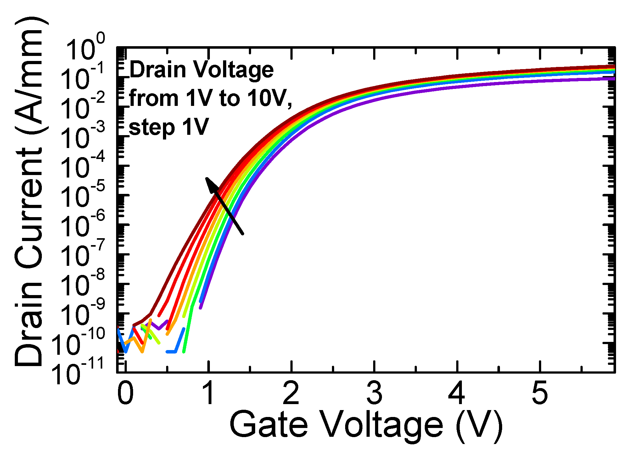
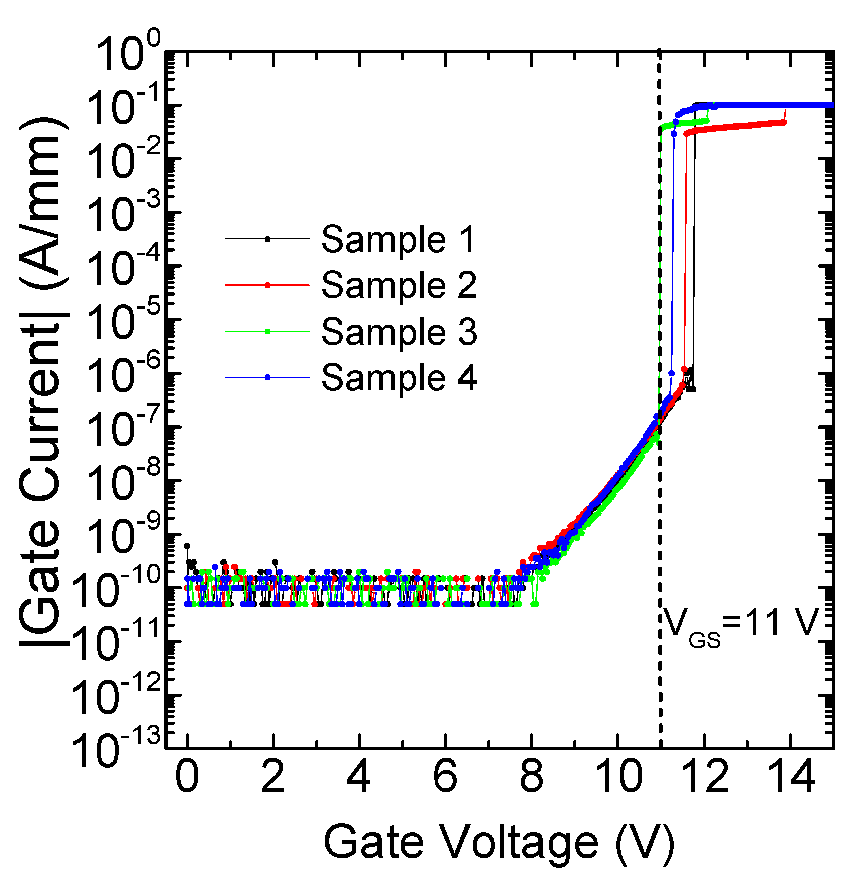
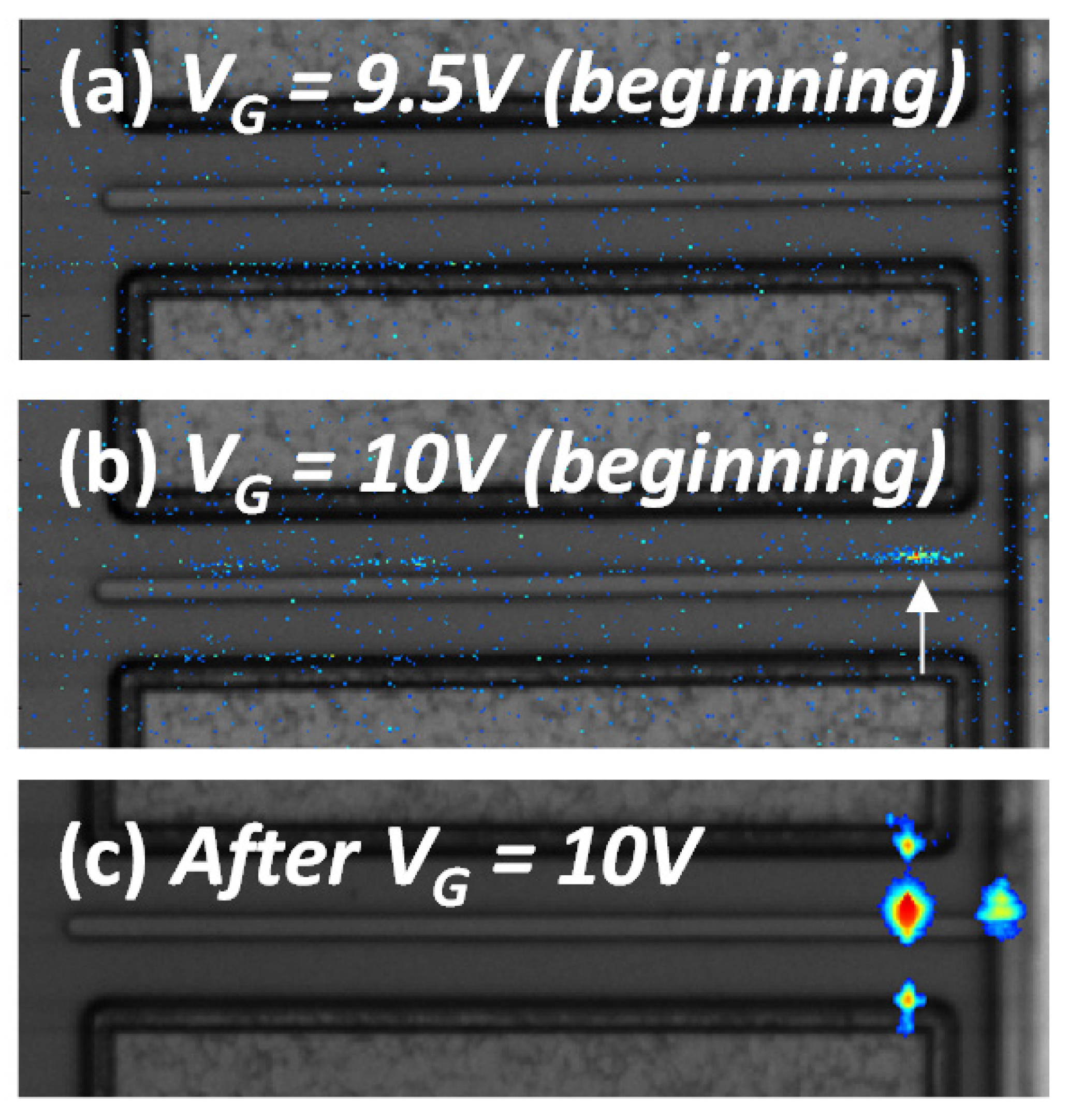
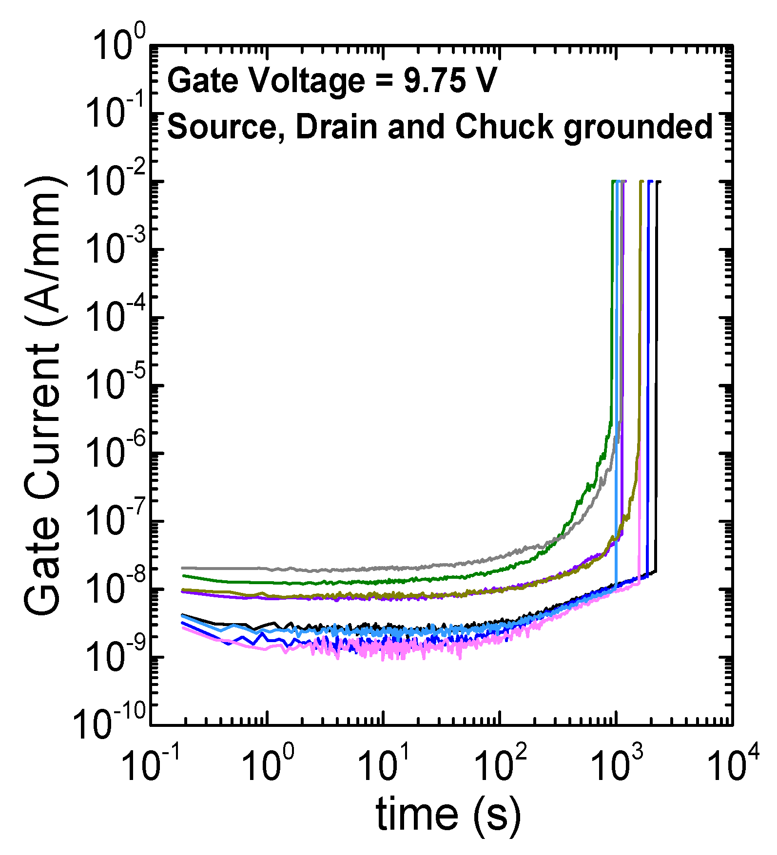
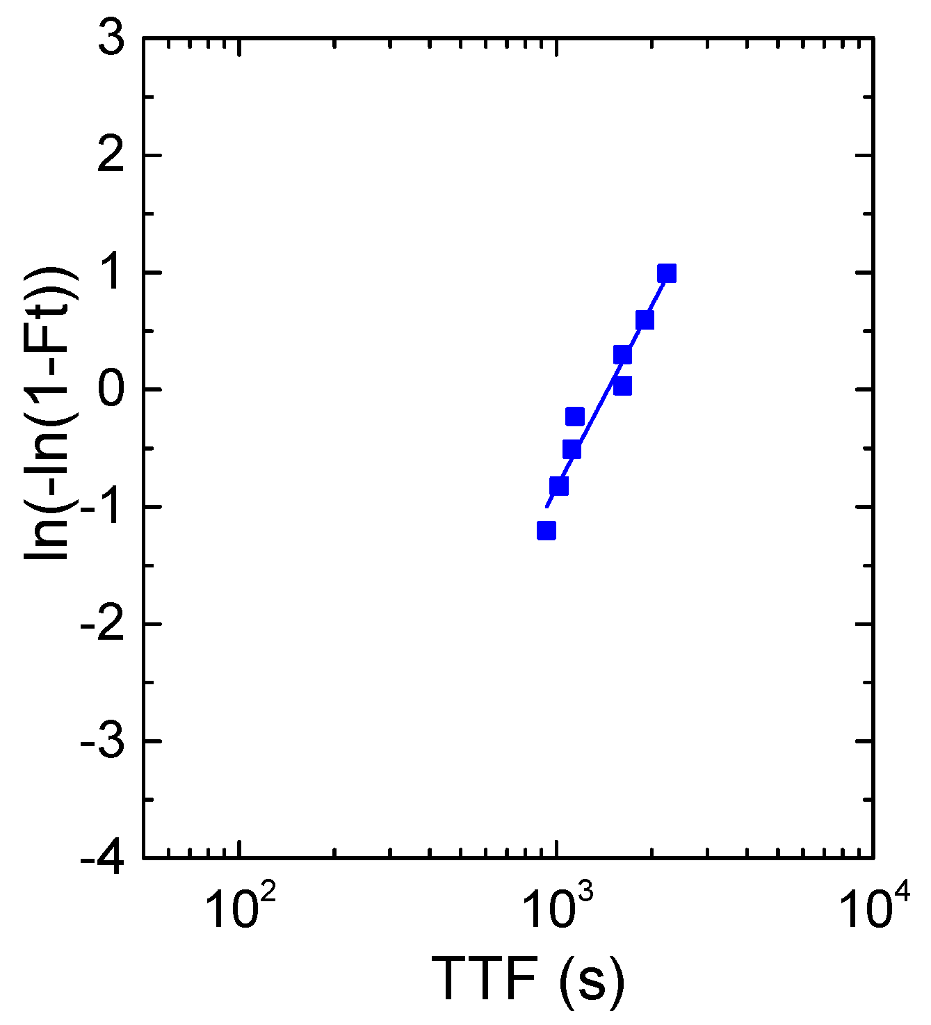
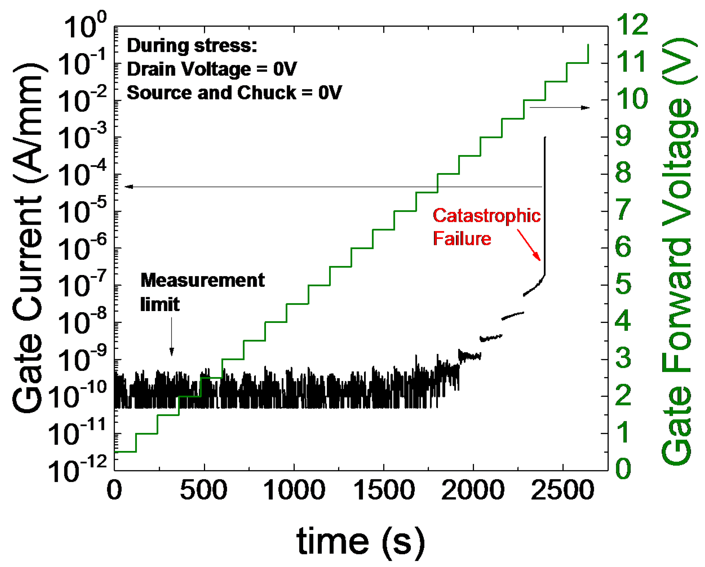
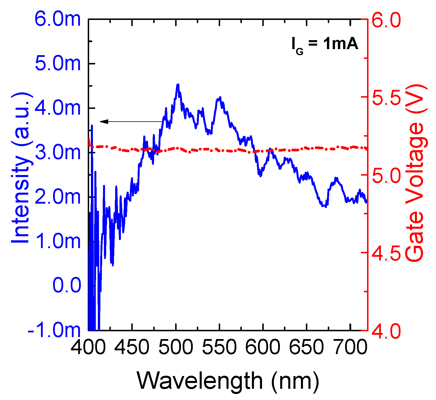
3. Results
- (i)
- at high (positive) gate bias, the electric field in the p-GaN can significantly increase (see the simulations in [13]), since the Schottky metal/p-GaN diode is reversely biased and the p-GaN is partly depleted. The high electric field can favor the generation of defects in the p-GaN, similarly to what observed in the AlGaN barrier under negative bias [15,18,19]. This may lead the generation of leakage paths and to the consequent failure of the gate junction. Avalanche effects (proposed in [13]) can further accelerate the defect generation process.
- (ii)
- during positive voltage stress the SiN passivation may be exposed to a high electric field, especially in proximity of the gate edge. This may lead to a time-dependent (and geometry-dependent) dielectric failure of SiN, with consequent increase in gate leakage.
4. Conclusions
Acknowledgments

Conflicts of Interest
References
- Moens, P.; Banerjee, A.; Uren, M.J.; Meneghini, M.; Karboyan, S.; Chatterjee, I.; Vanmeerbeek, P.; Cäsar, M.; Liu, C.; Salih, A.; et al. Impact of buffer leakage on intrinsic reliability of 650 V AlGaN/GaN HEMTs. In Proceedings of the 2015 IEEE International Electron Devices Meeting, Washington, DC, USA, 7–9 December 2015; pp. 903–906.
- Hilt, O.; Zhytnytska, R.; Böcker, J.; Bahat-treidel, E.; Brunner, F.; Knauer, A. 70 m Ω/600 V normally-off GaN transistors on SiC and Si substrates. In Proceedings of the 2015 IEEE 27th International Symposium on Power Semiconductor Devices & IC’s, Hong Kong, China, 10–14 May 2015; pp. 237–240.
- Ishida, M.; Ueda, T.; Tanaka, T.; Ueda, D. GaN on Si technologies for power switching devices. IEEE Trans. Electron. Devices 2013, 60, 3053–3059. [Google Scholar] [CrossRef]
- Wu, T.; Marcon, D.; de Jaeger, B.; van Hove, M.; Bakeroot, B.; Lin, D.; Kang, X.; Roelofs, R.; Groeseneken, G.; Decoutere, S. The impact of the gate dielectric quality in developing Au-free D-mode and E-mode recessed gate AlGaN/GaN transistors on a 200mm Si substrate. In Proceedings of the 2015 IEEE 27th International Symposium on Power Semiconductor Devices & IC’s, Hong Kong, China, 10–14 May 2015; pp. 225–228.
- Chen, K.J.; Yuan, L.; Wang, M.J.; Chen, H.; Huang, S.; Zhou, Q.; Zhou, C.; Li, B.K.; Wang, J.N. Physics of fluorine plasma ion implantation for GaN normally-off HEMT technology. In Proceedings of the IEEE International Electron Devices Meeting, Washington, DC, USA, 5–7 December 2011; pp. 465–468.
- Uemoto, Y.; Hikita, M.; Ueno, H.; Matsuo, H.; Ishida, H.; Yanagihara, M.; Ueda, T.; Tanaka, T.; Ueda, D. Gate injection transistor (GIT)—A normally-off AlGaN/GaN power transistor using conductivity modulation. IEEE Trans. Electron. Devices 2007, 54, 3393–3399. [Google Scholar] [CrossRef]
- Zanandrea, A.; Bahat-Treidel, E.; Rampazzo, F.; Stocco, A.; Meneghini, M.; Zanoni, E.; Hilt, O.; Ivo, P.; Wuerfl, J.; Meneghesso, G. Single- and double-heterostructure GaN-HEMTs devices for power switching applications. Microelectron. Reliab. 2012, 52, 2426–2430. [Google Scholar] [CrossRef]
- Huang, X.; Liu, Z.; Li, Q.; Lee, F.C. Evaluation and application of 600 v GaN HEMT in cascode structure. IEEE Trans. Power Electron. 2014, 29, 2453–2461. [Google Scholar] [CrossRef]
- Liu, C.; Wang, H.; Yang, S.; Lu, Y.; Liu, S.; Tang, Z.; Jiang, Q.; Huang, S.; Chen, K.J. Normally-off GaN MIS-HEMT with improved thermal stability in DC and dynamic performance. In Proceedings of the 2015 IEEE 27th International Symposium on Power Semiconductor Devices & IC’s, Hong Kong, china, 10–14 May 2015; pp. 213–216.
- Bisi, D.; Meneghini, M.; Stocco, A.; Cibin, G.; Pantellini, A.; Nanni, A.; Lanzieri, C.; Zanoni, E.; Meneghesso, G. Influence of fluorine-based dry etching on electrical parameters of AlGaN/GaN-on-Si high electron mobility transistors. In Proceedings of the European Solid-State Device Research Conference, Bucharest, Romania, 16–20 September 2013; pp. 61–64.
- Meneghini, M.; Member, S.; Rossetto, I.; Hurkx, F.; Šonský, J.; Croon, J.A.; Meneghesso, G.; Zanoni, E. Extensive Investigation of time-dependent breakdown of GaN-HEMTs submitted to OFF-state stress. IEEE Trans. Electron. Devices 2015, 62, 2549–2554. [Google Scholar] [CrossRef]
- Wu, T.; Marcon, D.; de Jaeger, B.; van Hove, M.; Bakeroot, B.; Stoffels, S.; Groeseneken, G.; Decoutere, S.; Roelofs, R. Time dependent dielectric breakdown (TDDB) evaluation of PE-ALD SiN gate dielectrics on AlGaN/GaN recessed gate D-mode MIS-HEMTs and E-mode MIS-FETs. In Proceedings of the IEEE International Reliability Physics Symposium, Monterey, CA, USA, 19–23 April 2015; pp. 4–9.
- Wu, T.; Member, S.; Marcon, D.; You, S.; Posthuma, N.; Bakeroot, B.; Stoffels, S.; van Hove, M.; Groeseneken, G.; Decoutere, S. Forward bias gate breakdown mechanism in enhancement-mode p-GaN gate AlGaN/GaN high-electron mobility transistors. IEEE Electron. Device Lett. 2015, 36, 1001–1003. [Google Scholar] [CrossRef]
- Ťapajna, M.; Hilt, O.; Würfl, J.; Kuzmík, J. Investigation of gate-diode degradation in normally-off p-GaN/AlGaN/GaN high-electron-mobility transistors. Appl. Phys. Lett. 2015, 107. [Google Scholar] [CrossRef]
- Meneghini, M.; Stocco, A.; Bertin, M.; Marcon, D.; Chini, A.; Meneghini, M.; Stocco, A.; Bertin, M.; Marcon, D.; Chini, A.; et al. Time-dependent degradation of AlGaN/GaN high electron mobility transistors under reverse bias. Appl. Phys. Lett. 2012, 100. [Google Scholar] [CrossRef]
- Meneghesso, G.; Rossi, F.; Salviati, G.; Uren, M.J.; Muoz, E.; Zanoni, E. Correlation between kink and cathodoluminescence spectra in AlGaN/GaN high electron mobility transistors. Appl. Phys. Lett. 2010, 96, 10–13. [Google Scholar] [CrossRef]
- Joh, J.; Gao, F.; Palacios, T.; del Alamo, J.A. A model for the critical voltage for electrical degradation of GaN high electron mobility transistors. Microelectron. Reliab. 2010, 50, 767–773. [Google Scholar] [CrossRef]
- Marcon, D.; Viaene, J.; Favia, P.; Bender, H.; Kang, X.; Lenci, S.; Stoffels, S.; Decoutere, S. Reliability of AlGaN/GaN HEMTs: Permanent leakage current increase and output current drop. In Proceedings of the International Symposium on the Physical and Failure Analysis of Integrated Circuits (IPFA), Suzhou, China, 15–19 July 2013; pp. 249–254.
- Marcon, S.D.D.; Meneghesso, G.; Wu, T.L.; Stoffels, S.; Meneghini, M. Reliability analysis of permanent degradations on AlGaN/GaN HEMTs. IEEE Trans. Electron. Devices 2013, 60, 3132–3141. [Google Scholar] [CrossRef]


© 2016 by the authors; licensee MDPI, Basel, Switzerland. This article is an open access article distributed under the terms and conditions of the Creative Commons by Attribution (CC-BY) license (http://creativecommons.org/licenses/by/4.0/).
Share and Cite
Meneghini, M.; Rossetto, I.; Rizzato, V.; Stoffels, S.; Van Hove, M.; Posthuma, N.; Wu, T.-L.; Marcon, D.; Decoutere, S.; Meneghesso, G.; et al. Gate Stability of GaN-Based HEMTs with P-Type Gate. Electronics 2016, 5, 14. https://doi.org/10.3390/electronics5020014
Meneghini M, Rossetto I, Rizzato V, Stoffels S, Van Hove M, Posthuma N, Wu T-L, Marcon D, Decoutere S, Meneghesso G, et al. Gate Stability of GaN-Based HEMTs with P-Type Gate. Electronics. 2016; 5(2):14. https://doi.org/10.3390/electronics5020014
Chicago/Turabian StyleMeneghini, Matteo, Isabella Rossetto, Vanessa Rizzato, Steve Stoffels, Marleen Van Hove, Niels Posthuma, Tian-Li Wu, Denis Marcon, Stefaan Decoutere, Gaudenzio Meneghesso, and et al. 2016. "Gate Stability of GaN-Based HEMTs with P-Type Gate" Electronics 5, no. 2: 14. https://doi.org/10.3390/electronics5020014
APA StyleMeneghini, M., Rossetto, I., Rizzato, V., Stoffels, S., Van Hove, M., Posthuma, N., Wu, T.-L., Marcon, D., Decoutere, S., Meneghesso, G., & Zanoni, E. (2016). Gate Stability of GaN-Based HEMTs with P-Type Gate. Electronics, 5(2), 14. https://doi.org/10.3390/electronics5020014